

Paper Menu >>
Journal Menu >>
 Optics and Photonics Journal, 2011, 1, 151-154 doi:10.4236/opj.2011.14025 Published Online December 2011 (http://www.SciRP.org/journal/opj) Copyright © 2011 SciRes. OPJ Design of a Silicon Overlay Glass Waveguide Sensor Kristian E. Medri, Robert C. Gauthier Department of Electronics, Carleton University, Ottawa, Canada E-mail: [email protected] Received August 13, 2011; revised Sep t ember 12, 2011; acc e pt ed September 24, 2011 Abstract A glass based slab waveguide, coated with a thin patterned high dielectric overlay, is configured into a re- fractive index sensor. The asymmetric nature of the waveguide configuration is exploited by keeping the mode in the slab waveguide while enhancing the field level in the overlay-superstrate. The sensor's response is examined using the FDTD simulation technique. A sensitivity of up to one part in 105 in the index of re- fraction discrimination is determined. The nature of the sensor ensures optical fibre compatibility, requires sub-µL sample volumes and provides a high resolution. Keywords: Refractive Index Sensor, Slab Waveguide, Patterned High Dielectric Overlay, FDTD, Integrated Optics 1. Introduction Silica based planar lightwave circuits (PLCs) evolved from simple passive waveguide structures to complex active devices containing resonators and filters.[1,2] When interfaced with optical fibers, PLCs can demon- strate low insertion losses due to th e compatibility of the materials, large modal overlap and relaxed manufactur- ing tolerances. In general, glass based integrated optics demonstrate a slow response when configured as active devices and are large due to the limited dielectric con- trast between guiding and substrate-superstrate layers. In the near and distant future it is expected that the optical fiber will continue to dominate as the signal carrying medium for optical telecommunications and sensing. The inter-compatibility requirements of active and passive integrated-optic devices and the optical fibre technology will remain. This will require low loss, low insertion loss, and fast IO components. These requirements can be met by a glass based waveguide design as the light guiding region, to minimize fibre coupling and insertion losses, then adding a thin high dielectric overlay of patterned silicon at the waveguide superstrate interface to retain the high dielectric contrast and response speed. This re- sults in a hybrid platform of silica and silicon akin to a strip loaded waveguide. Refractive index sensors can be used for many appli- cations. Previously proposed sensors which have similar footprints and responsiv ities include a 13 um sensor pro- viding 90 nm/RIU[3] and an 8 um sensor providing 130 nm/RIU [4] which have small non fiber compatible mode sizes. The researchers of the former include a compari- son to alternative sensing structures while the latter men- tions a much longer 173 um sensor providing a lower resolution of 33 nm/RIU [5]. This longer sensor has a larger mode size. They mention the option of using a 10 um plasmon sensor providing 465nm/RIU but with a large 10 dB loss. In order to demonstrate the principles involved in this hybrid waveguide configuration we employ a slab wave- guide in glass and a silicon overlay patterned as a Bragg grating [6]. The functionality is explored by examining the structure’s performance as an index of refraction sensor sensitized to the sensing region comprised of the superstrate region above the grating as well as in the etched regions of the grating. The next section presents the design of the sensor and discusses the modeling te- chnique employed. The sensor’s performance is then pre- sented. 2. Design The simplest planar optical structure is the traditional three layer glass slab waveguide (superstrate-waveguide -substrate), modified here into a 4 layer structure by adding a thin high dielectric overlay at the superstrate- waveguide interface (superstrate-overlay-wave-guide- substrate). The basic theory and analytical solution for the three layer structure is widely described [7,8] and has been extended to address multilayer structures with di- 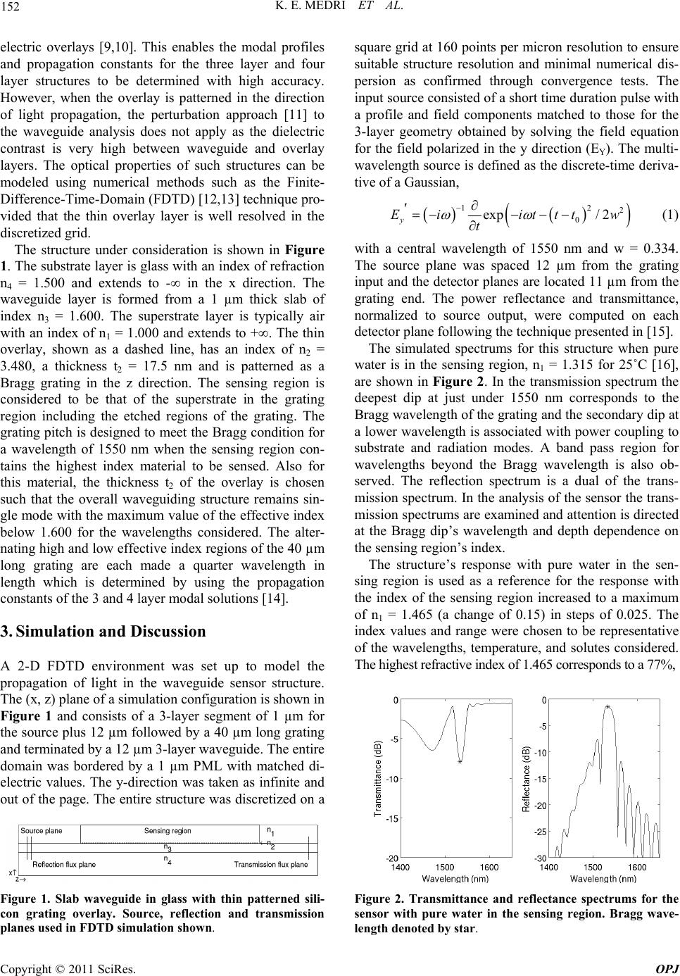 K. E. MEDRI ET AL. 152 electric overlays [9,10]. This enables the modal profiles and propagation constants for the three layer and four layer structures to be determined with high accuracy. However, when the overlay is patterned in the direction of light propagation, the perturbation approach [11] to the waveguide analysis does not apply as the dielectric contrast is very high between waveguide and overlay layers. The optical properties of such structures can be modeled using numerical methods such as the Finite- Difference-Time-Domain (FDTD) [12,13] technique pro- vided that the thin overlay layer is well resolved in the discretized grid. The structure under consideration is shown in Figure 1. The substrate layer is glass with an index of refraction n4 = 1.500 and extends to - in the x direction. The waveguide layer is formed from a 1 µm thick slab of index n3 = 1.600. The superstrate layer is typically air with an index of n1 = 1.000 and extends to +. The thin overlay, shown as a dashed line, has an index of n2 = 3.480, a thickness t2 = 17.5 nm and is patterned as a Bragg grating in the z direction. The sensing region is considered to be that of the superstrate in the grating region including the etched regions of the grating. The grating pitch is designed to meet the Bragg condition for a wavelength of 1550 nm when the sensing region con- tains the highest index material to be sensed. Also for this material, the thickness t2 of the overlay is chosen such that the overall waveguiding structure remains sin- gle mode with the maximum valu e of the effective index below 1.600 for the wavelengths considered. The alter- nating high and low effective index regions of the 40 µm long grating are each made a quarter wavelength in length which is determined by using the propagation constants of the 3 and 4 layer modal solutions [14]. 3. Simulation and Discussion A 2-D FDTD environment was set up to model the propagation of light in the waveguide sensor structure. The (x, z) plane of a simulation configuration is shown in Figure 1 and consists of a 3-layer segment of 1 µm for the source plus 12 µm followed by a 40 µm long grating and terminated by a 12 µm 3-layer waveguide. The entire domain was bordered by a 1 µm PML with matched di- electric values. The y-direction was taken as infinite and out of the page. The entire structure was discretized on a Figure 1. Slab waveguide in glass with thin patterned sili- con grating overlay. Source, reflection and transmission planes used in FDTD simulation shown. square grid at 160 points per micron resolution to ensure suitable structure resolution and minimal numerical dis- persion as confirmed through convergence tests. The input source cons isted of a short time dur ation pulse with a profile and field components matched to those for the 3-layer geometry obtained by solving the field equation for the field polarized in the y direction (EY). The multi- wavelength source is defined as the discrete-time deriva- tive of a Gaussian, 2 12 0 exp/ 2 y Ei itttw t (1) with a central wavelength of 1550 nm and w = 0.334. The source plane was spaced 12 µm from the grating input and the detecto r planes are located 11 µm from the grating end. The power reflectance and transmittance, normalized to source output, were computed on each detector plane following the technique presented in [15]. The simulated spectrums for this structure when pure water is in the sensing region, n1 = 1.315 for 25˚C [16], are shown in Figure 2. In the transmission spectrum the deepest dip at just under 1550 nm corresponds to the Bragg wavelength of the grating and the secondary dip at a lower wavelength is associated with power coupling to substrate and radiation modes. A band pass region for wavelengths beyond the Bragg wavelength is also ob- served. The reflection spectrum is a dual of the trans- mission spectrum. In the analysis of the sensor the trans- mission spectrums are examined and attention is directed at the Bragg dip’s wavelength and depth dependence on the sensing region’s index. The structure’s response with pure water in the sen- sing region is used as a reference for the response with the index of the sensing region increased to a maximum of n1 = 1.465 (a change of 0.15) in steps of 0.025. The index values and range were chosen to be representative of the wavelengths, temperature, and solutes considered. The highest refractive index of 1.465 corresponds to a 77%, Figure 2. Transmittance and reflectance spectrums for the sensor with pure water in the sensing region. Bragg wave- length denoted by star. Copyright © 2011 SciRes. OPJ 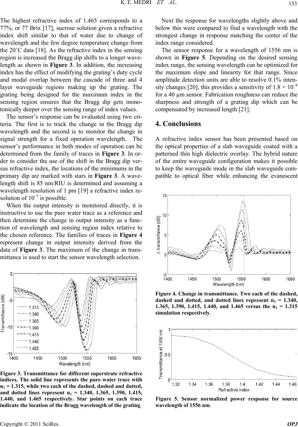 153 K. E. MEDRI ET AL. The highest refractive index of 1.465 corresponds to a 77%, or 77 Brix [17], sucrose solution given a refractive index shift similar to that of water due to change of wavelength and the few degree temperature change from the 20˚C data [18]. As the refractive index in the sensing region is increased the Bragg dip shifts to a longer wave- length as shown in Figure 3. In addition, the increasing index has the effect of modifying the grating’s duty cycle and modal overlap between the cascade of three and 4 layer waveguide regions making up the grating. The grating being designed for the maximum index in the sensing region ensures that the Bragg dip gets mono- tonically deeper over the sensing range of index values. The sensor’s response can be evaluated using two cri- teria. The first is to track the change in the Bragg dip wavelength and the second is to monitor the change in signal strength for a fixed operation wavelength. The sensor’s performance in both modes of operation can be determined from the family of traces in Figure 3. In or- der to consider the use of the shift in the Bragg dip ver- sus refractive index, th e locatio ns of th e mini mu ms in th e primary dip are marked with stars in Figure 3. A wave- length shift is 85 nm/RIU is determined and assuming a wavelength resolution of 1 pm [19] a refractive index re- solution of 10–5 is possible. When the output intensity is monitored directly, it is instructive to use the pure water trace as a reference and then determine the change in output intensity as a func- tion of wavelength and sensing region index relative to the chosen reference. The families of traces in Figure 4 represent change in output intensity derived from the data of Figure 3. The maximum of the change in trans- mittance is used to start the sensor waveleng th selection. Figure 3. Transmittance for different superstrate refractive indices. The solid line represents the pure water trace with n1 = 1.315, while two each of the dashed, dashed and dotted, and dotted lines represent n1 = 1.340, 1.365, 1.390, 1.415, 1.440, and 1.465 respectively. Star points on each trace indicate the location of the Bragg wavelength of the grating. Next the response for wavelengths slightly above and below this were compared to find a wavelength with the strongest change in response matching the center of the index range considered. The sensor response for a wavelength of 1556 nm is shown in Figure 5. Depending on the desired sensing index range, the sensing wavelength can be optimized for the maximum slope and linearity for that range. Since amplitude detection units are able to resolve 0.1% inten- sity changes [20], this provides a sen sitivity of 1.8 × 10⁻⁴ for a 40 µm sensor. Fabrication roughness can reduce the sharpness and strength of a grating dip which can be compensated by increased length [21]. 4. Conclusions A refractive index sensor has been presented based on the optical properties of a slab waveguide coated with a patterned thin high dielectric overlay. The hybrid nature of the entire waveguide configuration makes it possible to keep the waveguid e mode in the slab wavegu ide com- patible to optical fiber while enhancing the evanescent Figure 4. Change in transmittance. Two each of the dashed, dashed and dotted, and dotted lines represent n1 = 1.340, 1.365, 1.390, 1.415, 1.440, and 1.465 versus the n1 = 1.315 simulation respectively. Figure 5. Sensor normalized power response for source wavelength of 1556 nm. Copyright © 2011 SciRes. OPJ 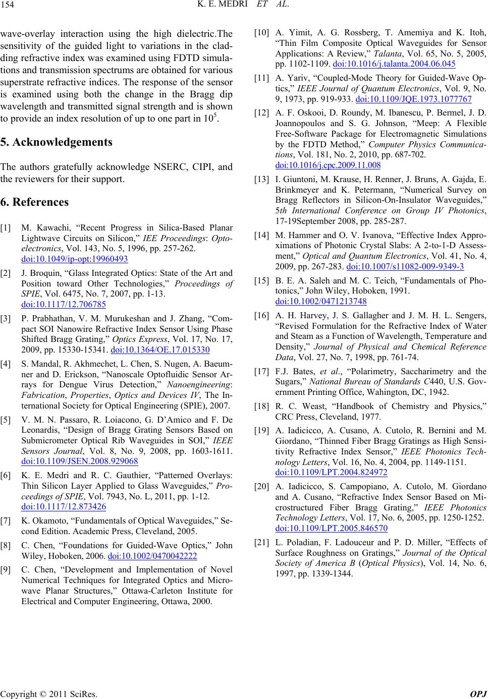 K. E. MEDRI ET AL. Copyright © 2011 SciRes. OPJ 154 wave-overlay interaction using the high dielectric.The sensitivity of the guided light to variations in the clad- ding refractive index was examined us ing FDTD simula- tions and transmission spectrums are obtained for various superstrate refractive indices. The response of the sensor is examined using both the change in the Bragg dip wavelength and transmitted signal strength and is shown to provide an index resolution of up to one part in 105. 5. Acknowledgements The authors gratefully acknowledge NSERC, CIPI, and the reviewers for their support. 6. References [1] M. Kawachi, “Recent Progress in Silica-Based Planar Lightwave Circuits on Silicon,” IEE Proceedings: Opto- electronics, Vol. 143, No. 5, 1996, pp. 257-262. doi:10.1049/ip-opt:19960493 [2] J. Broquin, “Glass Integrated Optics: State of the Art and Position toward Other Technologies,” Proceedings of SPIE, Vol. 6475, No. 7, 2007, pp. 1-13. doi:10.1117/12.706785 [3] P. Prabhathan, V. M. Murukeshan and J. Zhang, “Com- pact SOI Nanowire Refractive Index Sensor Using Phase Shifted Bragg Grating,” Optics Express, Vol. 17, No. 17, 2009, pp. 15330-15341. doi:10.1364/OE.17.015330 [4] S. Mandal, R. Akhmechet, L. Chen, S. Nugen, A. Baeum- ner and D. Erickson, “Nanoscale Optofluidic Sensor Ar- rays for Dengue Virus Detection,” Nanoengineering: Fabrication, Properties, Optics and Devices IV, The In- ternational Society for Optical Engineering (SPIE), 2007. [5] V. M. N. Passaro, R. Loiacono, G. D’Amico and F. De Leonardis, “Design of Bragg Grating Sensors Based on Submicrometer Optical Rib Waveguides in SOI,” IEEE Sensors Journal, Vol. 8, No. 9, 2008, pp. 1603-1611. doi:10.1109/JSEN.2008.929068 [6] K. E. Medri and R. C. Gauthier, “Patterned Overlays: Thin Silicon Layer Applied to Glass Waveguides,” Pro- ceedings of SPIE, Vol. 7943, No. L, 2011, pp. 1-12. doi:10.1117/12.873426 [7] K. Okamoto, “Fundamentals of Optical Waveguides,” Se- cond Edition. Academic Press, Cleveland, 2005. [8] C. Chen, “Foundations for Guided-Wave Optics,” John Wiley, Hoboken, 2006. doi:10.1002/0470042222 [9] C. Chen, “Development and Implementation of Novel Numerical Techniques for Integrated Optics and Micro- wave Planar Structures,” Ottawa-Carleton Institute for Electrical and Computer Engineering, Ottawa, 2000. [10] A. Yimit, A. G. Rossberg, T. Amemiya and K. Itoh, “Thin Film Composite Optical Waveguides for Sensor Applications: A Review,” Talanta, Vol. 65, No. 5, 2005, pp. 1102-1109. doi:10.1016/j.talanta.2004.06.045 [11] A. Yariv, “Coupled-Mode Theory for Guided-Wave Op- tics,” IEEE Journal of Quantum Electronics, Vol. 9, No. 9, 1973, pp. 919-933. doi:10.1109/JQE.1973.1077767 [12] A. F. Oskooi, D. Roundy, M. Ibanescu, P. Bermel, J. D. Joannopoulos and S. G. Johnson, “Meep: A Flexible Free-Software Package for Electromagnetic Simulations by the FDTD Method,” Computer Physics Communica- tions, Vol. 181, No. 2, 2010, pp. 687-702. doi:10.1016/j.cpc.2009.11.008 [13] I. Giuntoni, M. Krause, H. Renner, J. Bruns, A. Gajda, E. Brinkmeyer and K. Petermann, “Numerical Survey on Bragg Reflectors in Silicon-On-Insulator Waveguides,” 5th International Conference on Group IV Photonics, 17-19September 2008, pp. 285-287. [14] M. Hammer and O. V. Ivanova, “Effective Index Appro- ximations of Photonic Crystal Slabs: A 2-to-1-D Assess- ment,” Optical and Quantum Electronics, Vol. 41, No. 4, 2009, pp. 267-283. doi:10.1007/s11082-009-9349-3 [15] B. E. A. Saleh and M. C. Teich, “Fundamentals of Pho- tonics,” John Wiley, Hoboken, 1991. doi:10.1002/0471213748 [16] A. H. Harvey, J. S. Gallagher and J. M. H. L. Sengers, “Revised Formulation for the Refractive Index of Water and Steam as a Function of Wavelength, Temperature and Density,” Journal of Physical and Chemical Reference Data, Vol. 27, No. 7, 1998, pp. 761-74. [17] F.J. Bates, et al., “Polarimetry, Saccharimetry and the Sugars,” National Bureau of Standards C440, U.S. Gov- ernment Printing Office, Wahington, DC, 1942. [18] R. C. Weast, “Handbook of Chemistry and Physics,” CRC Press, Cleveland, 1977. [19] A. Iadicicco, A. Cusano, A. Cutolo, R. Bernini and M. Giordano, “Thinned Fiber Bragg Gratings as High Sensi- tivity Refractive Index Sensor,” IEEE Photonics Tech- nology Letters, Vol. 16, No. 4, 2004, pp. 1149-1151. doi:10.1109/LPT.2004.824972 [20] A. Iadicicco, S. Campopiano, A. Cutolo, M. Giordano and A. Cusano, “Refractive Index Sensor Based on Mi- crostructured Fiber Bragg Grating,” IEEE Photonics Technology Letters, Vol. 17, No. 6, 2005, pp. 1250-1252. doi:10.1109/LPT.2005.846570 [21] L. Poladian, F. Ladouceur and P. D. Miller, “Effects of Surface Roughness on Gratings,” Journal of the Optical Society of America B (Optical Physics), Vol. 14, No. 6, 1997, pp. 1339-1344. |