

Paper Menu >>
Journal Menu >>
 Circuits and Systems, 2011, 2, 293-296 doi:10.4236/cs.2011.24041 Published Online October 2011 (http://www.scirp.org/journal/cs) Copyright © 2011 SciRes. CS Study and Enhanced Design of RF Dual Band Bandpass Filter Validation and Confirmation of Experimental Measurements Mohamed Mabrouk, Leila Bousbia CIRTACOM and ISETCOM of Tunis, University of Carthage, Tunis, Tunisia E-mail: [email protected] Received July 22, 201 1; revised August 12, 2011; accepted August 21, 2011 Abstract Dual band bandpass filter is designed and optimized for RF wireless applications. The performances of that RF dual band filter are improved especially parameters describing the insertion loss, return losses and rejec- tion. Dual band bandpass filter using stub loaded resonators is designed and characterized. Theoretical re- sults are compared with experimental data. This comparison shows that the magnitude of reflection coeffi- cient S11 from ADSTM simulation is better than 28.0 dB, and the insertion loss S21 is less than 0.5 dB. The two rejections are also better than 32.0 dB. The simulated results also show that two central frequencies are located at desired 1.82 and 2.95 GHz. Comparison of measured and simulated results shows frequency drift. The main reason for this frequency shifting is due to some uncertainties. These are obviously due to geomet- rical and physical parameters H and r respectively of Duroid substrate used during design and measure- ments. Keywords: RF Filters, Dual Bandpass, Effective Permittivity, Physical and Geometrical Parameters 1. Introduction RF circuits with a dual pass band operation are required by modern wireless communication systems [1]. For example, the RF transceiver length (TX/RX) for second generation GSM and third-generation WCDMA mobile communications must be able to receive and transmit 900 MHz and 1900 MHz signals. Also 2.4 GHz and 5.2 GHz bands are two bands operated by high-speed wireless LANs [1,2]. The band pass filter is necessary to generate two or more transmission frequency bands, in particular dual-band filters, as they hav e an essential role in transmit-receive systems [2]. RF filters have par- ticularly an important role for signals filtering, rejection and isolation between parts in transceivers systems (TX/RX). Filters have the characteristic to be frequency selective devices for transmitting and attenuating signal in desired frequency ranges [3] Many different ways are considered to design dual- band bandpass filters such combination of two filters operating on two different bandwidths [4] and using dual band stepped impedances resonator [5] or dual band stubs resonators [6]. Quasi lumped with open loop band pass filters operating at different frequency bands [7] and using square loop dual mode resonators [8] are also used for designing this type of filters. Small insertion loss, low return loss and high rejection band are the desired characteristics of a good filter. The design of this kind of filter is considered using electromagnetic (EM) simu- lators. The studied filter was simulated usin g IE3DTM [6], and in this paper we report our ADSTM simulation optimized results which are very close to the experimental measurements. ADSTM software has been used succe- ssfully many times for simulation design filter so th at the resulting performances meet the microwave filter speci- fications. Simulated results confirm that two central frequencies are located at desired values 1.82 GHz and 2.95 GHz. 2. Design Description of Band Pass Filter The studied filter is composed of two ring-resonators loaded with two open stubs. Figure 1 shows the physical layout of the dual band pass filter using uniform microstrip lines. This filter consists of two microstrip open loops. Two open circuited stubs are attached [6] at 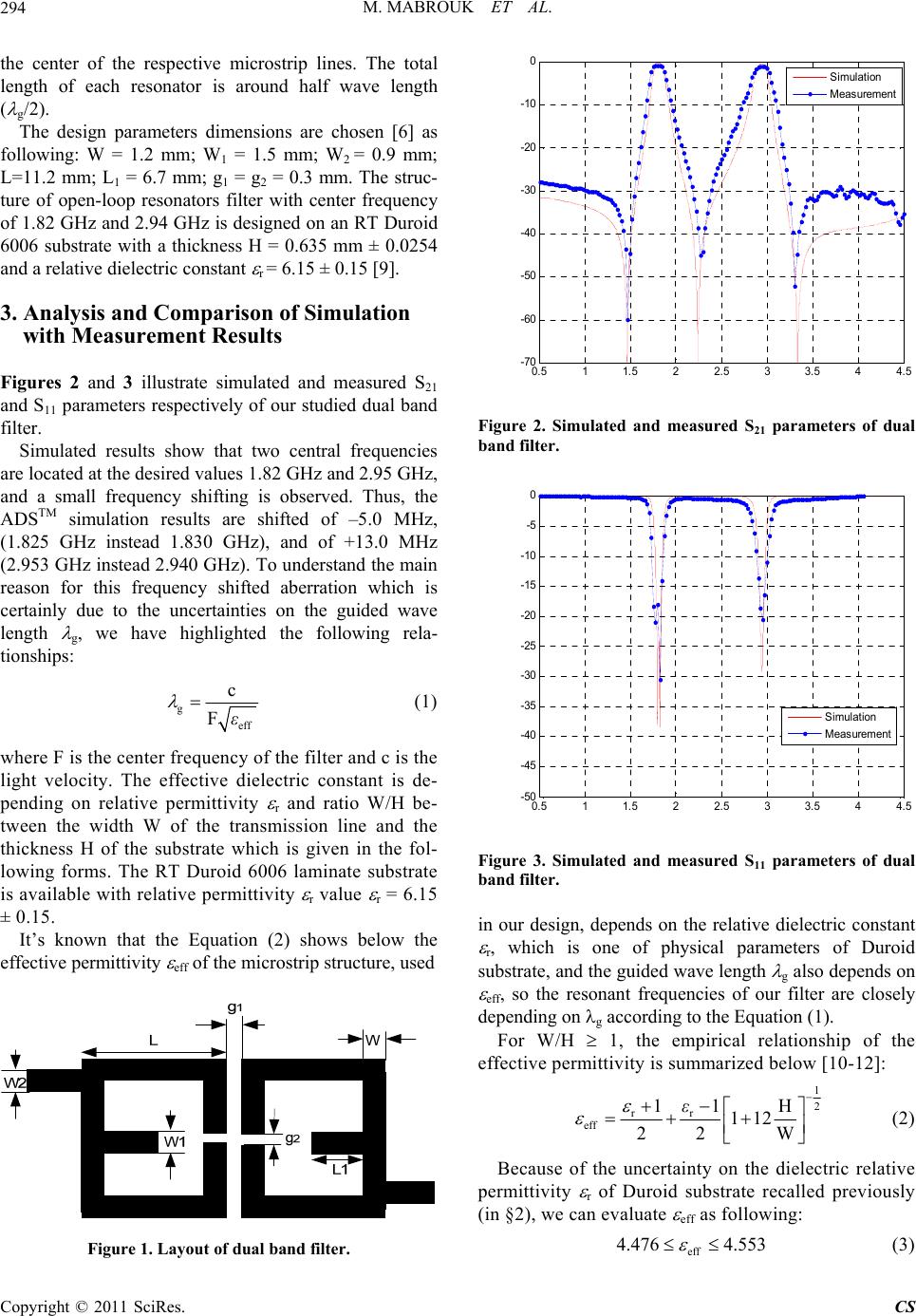 M. MABROUK ET AL. 294 the center of the respective microstrip lines. The total length of each resonator is around half wave length ( g/2). The design parameters dimensions are chosen [6] as following: W = 1.2 mm; W1 = 1.5 mm; W2 = 0.9 mm; L=11.2 mm; L1 = 6.7 mm; g1 = g2 = 0.3 mm. The struc- ture of open-loop resonators filter with center frequency of 1.82 GHz and 2.94 GHz is de signed on an RT Duroid 6006 substrate with a thickness H = 0.635 mm ± 0.0254 and a relative dielectric constant r = 6.15 ± 0.15 [9]. 3. Analysis and Comparison of Simulation with Measurement Results Figures 2 and 3 illustrate simulated and measured S21 and S11 parameters respectively of our studied dual band filter. Simulated results show that two central frequencies are located at the desired values 1.82 GHz and 2.95 GHz, and a small frequency shifting is observed. Thus, the ADSTM simulation results are shifted of –5.0 MHz, (1.825 GHz instead 1.830 GHz), and of +13.0 MHz (2.953 GHz instead 2.940 GHz). To understand the main reason for this frequency shifted aberration which is certainly due to the uncertainties on the guided wave length g, we have highlighted the following rela- tionships: g eff c F ε 1 where F is the center frequency of the filter and c is the light velocity. The effective dielectric constant is de- pending on relative permittivity r and ratio WH be- tween the width W of the transmission line and the thickness H of the substrate which is given in the fol- lowing forms. The RT Duroid 6006 laminate substrate is available with relative permittivity r value r = 6.15 ± 0.15. It’s known that the Equation (2) shows below the effective permittivity eff of the microstrip structure, used Figure 1. Layout of dual band filter. 0.5 11.5 22.5 33.5 44.5 -70 -60 -50 -40 -30 -20 -10 0 Simulation Measurement Figure 2. Simulated and measured S21 parameters of dual band filter. 0.5 11.5 22.5 33.5 44.5 -50 -45 -40 -35 -30 -25 -20 -15 -10 -5 0 Simulation Mea surem ent Figure 3. Simulated and measured S11 parameters of dual band filter. in our design, depends on the relative dielectric constant r, which is one of physical parameters of Duroid substrate, and the guided wave length g also depends on eff, so the resonant frequencies of our filter are closely depending on g according to the Equation (1). For WH 1, the empirical relationship of the effective permittivity is summarized below [10-12]: 1 2 rr eff 11 H 112 22 W ε 2 Because of the uncertainty on the dielectric relative permittivity r of Duroid substrate recalled previously (in §2), we can evaluate eff as following : eff 4.476 4.553 3 Copyright © 2011 SciRes. CS 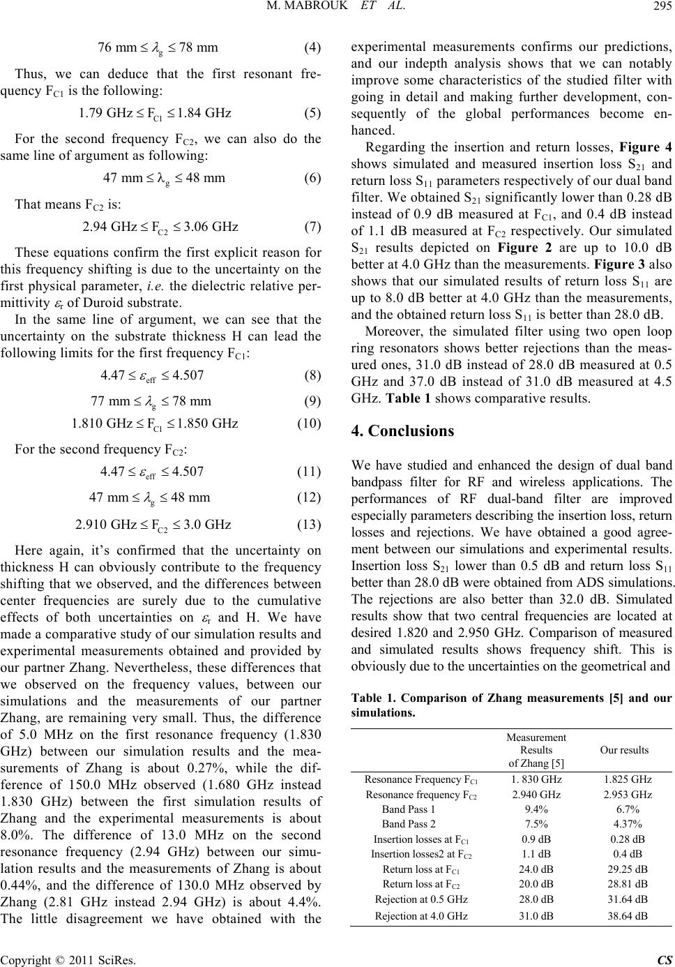 M. MABROUK ET AL.295 g 76 mm78 mm 4 Thus, we can deduce that the first resonant fre- quency FC1 is the following C1 1.79 GHzF1.84 GHz 5 For the second frequency FC2, we can also do the same line of argument as following g 47mm48 mm 6 That means FC2 is: C2 2.94 GHzF3.06 GHz 7 These equations confirm the first explicit reason for this frequency shifting is due to the uncertainty on the first physical parameter, i.e. the dielectric relative per- mittivity r of Duroid substrate. In the same line of argument, we can see that the uncertainty on the substrate thickness H can lead the following limits for the first frequency FC1: eff 4.47 4.507 8 g 77mm78mm 9 C1 1.810 GHzF1.850 GHz 10 For the second frequency FC2: eff 4.47 4.507 11 g 47mm48 mm 12 C2 2.910 GHzF3.0 GHz 13 Here again, it’s confirmed that the uncertainty on thickness H can obviously contribute to the frequency shifting that we observed, and the differences between center frequencies are surely due to the cumulative effects of both uncertainties on r and H. We have made a comparative study of our simulation results and experimental measurements obtained and provided by our partner Zhang. Nevertheless, these differences that we observed on the frequency values, between our simulations and the measurements of our partner Zhang, are remaining very small. Thus, the difference of 5.0 MHz on the first resonance frequency (1.830 GHz) between our simulation results and the mea- surements of Zhang is about 0.27%, while the dif- ference of 150.0 MHz observed (1.680 GHz instead 1.830 GHz) between the first simulation results of Zhang and the experimental measurements is about 8.0%. The difference of 13.0 MHz on the second resonance frequency (2.94 GHz) between our simu- lation results and the measurements of Zhang is about 0.44%, and the difference of 130.0 MHz observed by Zhang (2.81 GHz instead 2.94 GHz) is about 4.4%. The little disagreement we have obtained with the experimental measurements confirms our predictions, and our indepth analysis shows that we can notably improve some characteristics of the studied filter with going in detail and making further development, con- sequently of the global performances become en- hanced. Regarding the insertion and return losses, Figure 4 shows simulated and measured insertion loss S21 and return loss S11 parameters respectively of our dual band filter. We obtained S21 significantly lower than 0.28 dB instead of 0.9 dB measured at FC1, and 0.4 dB instead of 1.1 dB measured at FC2 respectively. Our simulated S21 results depicted on Figure 2 are up to 10.0 dB better at 4.0 GHz than the measurements. Figure 3 also shows that our simulated results of return loss S11 are up to 8.0 dB better at 4.0 GHz than the measurements, and the obtained return loss S11 is better than 28.0 dB. Moreover, the simulated filter using two open loop ring resonators shows better rejections than the meas- ured ones, 31.0 dB instead of 28.0 dB measured at 0.5 GHz and 37.0 dB instead of 31.0 dB measured at 4.5 GHz. Table 1 shows comparative results. 4. Conclusions We have studied and enhanced the design of dual band bandpass filter for RF and wireless applications. The performances of RF dual-band filter are improved especially parameters describing the insertion loss, return losses and rejections. We have obtained a good agree- ment between our simulations and experimental results. Insertion loss S21 lower than 0.5 dB and return loss S11 better than 28.0 dB were obtained from ADS simulations. The rejections are also better than 32.0 dB. Simulated results show that two central frequencies are located at desired 1.820 and 2.950 GHz. Comparison of measured and simulated results shows frequency shift. This is obviously due to the uncertainties on the geometrical and Table 1. Comparison of Zhang measurements [5] and our simulations. Measurement Results of Zhang [5] Our results Resonance Frequency FC1 1. 830 GHz 1.825 GHz Resonance frequency FC2 2.940 GHz 2.953 GHz Band Pass 1 9.4% 6.7% Band Pass 2 7.5% 4.37% Insertion losses at FC1 0.9 dB 0.28 dB Insertion losses2 at FC2 1.1 dB 0.4 dB Return loss at FC1 24.0 dB 29.25 dB Return loss at FC2 20.0 dB 28.81 dB Rejection at 0.5 GHz 28.0 dB 31.64 dB Rejection at 4.0 GHz 31.0 dB 38.64 dB Copyright © 2011 SciRes. CS  M. MABROUK ET AL. Copyright © 2011 SciRes. CS 296 0.5 11.5 22.5 33.5 44.5 -70 -60 -50 -40 -30 -20 -10 0 Frequency [GHz] Magnitude [dB] S 11 Simulation S 21 Simulation S 11 Meas ure me nt S 21 Meas ure me nt Figure 4. Simulated and measured S11, S21 parameters of dual-band filter. physical parameters H and r respectively of Duroid substrate used during design and measurements. 5. Acknowledgements The authors would like to acknowledge and extend their gratitude to our partner Xiu Yin Zhang, Associate Pro- fessor with the School of Electronic and Information Engineering (South China University of Technology, Guangzhou, 510641, China) who has carried out and provided the experimental measurements of studied pro- totype of filter. 6. References [1] C. Y. Chen, C. Y. Hsu and H. R. Chuong, “Design of Miniature Planar Dual Band Filter Using Dual-Feeding Structures and Embedded Resonators,” IEEE Microwave and Wireless Components Letters, Vol. 16, No. 12, 2006, pp. 669-671. doi:10.1109/LMWC.2006.885621 [2] S. F. Chang, Y. H. Jeng and J. L. Chen, “Dual-Band Step Impedance Band Pass Filter for Multimode Wireless LANs,” Electronic Letters, Vol. 40, No. 1, 2004, pp. 38-39. doi:10.1049/el:20040065 [3] I. C. Hunter, L. Billonet, B. Jarry and P. Guillon, “Micro- wave Filters—Applications and T echnology,” IEEE Micro- wave Theory and Techniques Transactions, Vol. 50, No. 3, March 2002, pp. 794-805. doi:10.1109/22.989963 [4] H. Miyake, S. Kitazawa, T. Ishizaki, T. Ymanda and Y. Nagatomi, “A Miniaturized Monolithic Dual-band Filter Using Ceramic Lamination Technique for Dual Mode Portable Telephones,” IEEE MTT-S International Micro- wave Symposium Digest, 8-13 June 1997, Vol. 2, pp. 789-792. [5] J. T. Kuo, T. H. Yeh and C. Yeh, “Design of Microstrip Bandpass Filters with a Dual Pass Band Response,” IEEE Microwave Theory and Techniques Transactions, Vol. 53, No. 4, April 2005, pp. 1331-1337. doi:10.1109/TMTT.2005.845765 [6] X. Y. Zhang, J. X. Chen and Q. Xue, “Dual-band Band Pass Filters Using Stub-Loaded Resonators,” IEEE Micro- wave and Wireless Components Letters, Vol. 17, No. 8, 2007, pp. 583-585. doi:10.1109/LMWC.2007.901768 [7] A. Balalem, W. Menzel and A. Omar, “Quasi Lumped Open Loop Suspended Stripline Bandpass Filters,” 36th European Microwave Conference, Manchester, 10-15 Sep- tember 2006, pp. 568-571. [8] A. Balalem, J. Machac and A. Omar, “Dual-band Bandpass Filter by Using Square Loop Dual Mode Resonator,” International Journal of Microwave and Optical Tech- nology, Vol. 50, No. 6, June 2008, pp. 1567-1570. doi:10.1002/mop.23427 [9] “RT/duroid® 6006/6010LM High Frequency Laminates,” 1998. http://www.rogerscorp.com/documents/612/acm/RT-duro id-6006-6010-laminate-data-sheet [10] M. V. Schneider, “Microstrip Lines for Microwave Inte- grated Circuits,” The Bell System Technical Journal, Vol. 48, No. 5, 1969, pp. 1421-1444. [11] H. A. Wheeler, “Transmission Line Properties of a Strip on a Dielectric Sheet on a Plane,” IEEE Microwave Theory and Techniques Transactions, Vol. 25, No. 8, 1977, pp. 631-647. doi:10.1109/TMTT.1977.1129179 [12] K. C. Gupta, et al., “Computer-Aided Design of Microwave Circuits ,” A rtech H ouse, D edh am , 1 981 , pp. 13 1-134 . |