
Paper Menu >>
Journal Menu >>
 Vol.3, No.9, 812-815 (2011) Natural Science http://dx.doi.org/10.4236/ns.2011.39106 Copyright © 2011 SciRes. OPEN ACCESS Effect of dislocation scattering on electron mobility in GaN R. Karthik, P. Uma Sathyakam, P. S. Mallick* School of Electrical Engineering, VIT University, Vellore, India; *Corresponding Author: [email protected] Received 21 July 2011; revised 24 August 2011; accepted 21 September 2011. ABSTRACT This paper presents the calculation of electron mobility of GaN at various temperatures using Relaxation Time Approximation (RTA) method. The effect of dislocation scattering on electron mobility in GaN is studied. We have discussed about the role of important scattering mecha- nisms in GaN. The electron mobility values thus obtained are compared with other available ex- perimental and theoretical results. Keywords: Dislocation Scattering; Electron Mobility; Galium Nitride; Scattering 1. INTRODUCTION Gallium Nitride, a direct bandgap semiconductor, has emerged as an important material for high-power, opto- electronic as well as for high temperature devices be- cause of its large bandgap (3.4 eV), strong bond strength (2.3 eV/bond) and high breakdown voltage (3 106 V/cm) [1]. Recently the material has become more popular because of several new applications including blue light emitting diodes and blue laser diodes [2]. GaN is normally grown either by metal-organic chemical va- por deposition (MOCVD), molecular beam epitaxy (MBE) or hybrid vapor phase epitaxy (HVPE) on sap- phire (Al2O3) or SiC substrate with large lattice mis- match. The most commonly used substrate is Al2O3 with 13.8% lattice mismatch and SiC substrate with 4% lattice mismatch. The large lattice mismatch with the substrate produces large amount of dislocation at the interfacial layer resulting very poor interface characteristic. As one moves away from the interfacial layer, the dislocation density decreases very fast. This means whole GaN epi- layer consists of two layers which was suggested by D. C. Look et al. [3]. In order to calculate the mobility in n- type GaN, we have considered the two layer model. For bulk layer away from the interface the dominant scatter- ing mechanisms are considered to be acoustic phonon scattering via deformation potential, piezoelectric cou- pling and non phonon scattering such as ionized impurity scattering and the neutral impurity scattering. On the contrary, the dominant scattering mechanism near the interfacial region is assumed to be dislocation scattering only. The electrical transport properties of the entire GaN epilayer would be influenced by dislocation scattering dominant near the interfacial region. Electron mobility in GaN and the effect of dislocation scattering on electron mobility in GaN were studied earlier by many resear- chers [3-7]. In this paper, we have considered all the im- portant scattering mechanisms of GaN in more detail using RTA to obtain electron mobility and we have also shown the difference between the electron mobility with and without dislocation scattering. 2. THEORY Solution of Boltzmann equation using RTA gives elec- tron mobility as, * e m (1) where, , is average relaxation time over the electron energies, is mobility and m* is the effective mass of electron. The expressions of relaxation time and mobility caused by different scattering mechanisms are given in the following sections. 2.1. Ionized Impurity Scattering The amount of scattering due to electrostatic forces between the carrier and the ionized impurity depends on the interaction time and the number of impurities. Larger impurity concentrations result in a lower mobility [8]. The standard formula for calculating the average relaxa- tion time is 32 0 0 *32 0 0 dd d e dd d ii ii f EE E E Ef mEE E (2) Hence the mobility associated with ionized impurity 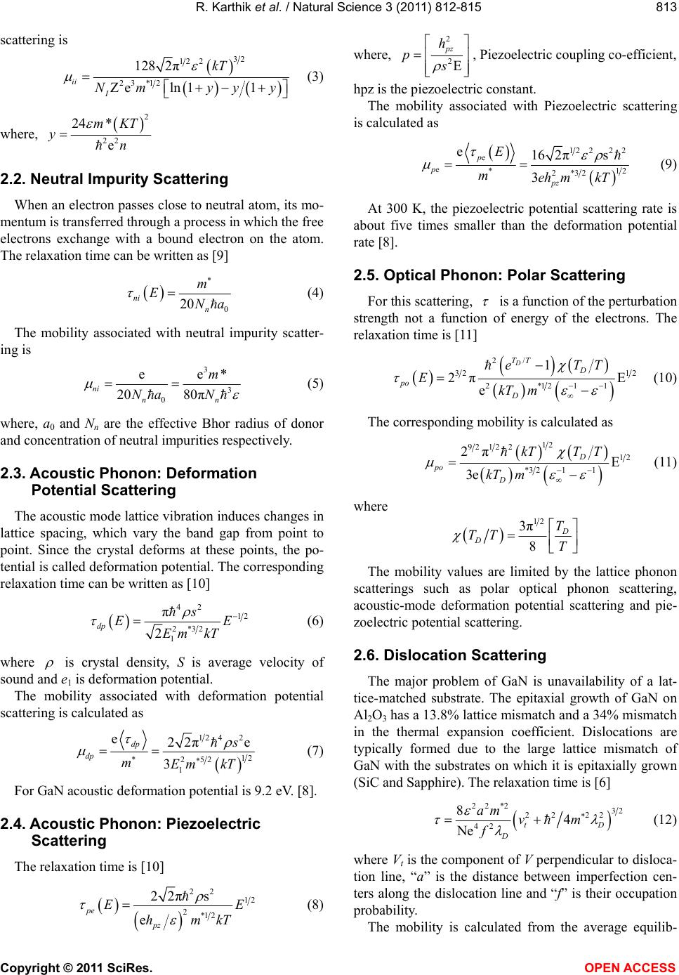 R. Karthik et al. / Natural Science 3 (2011) 812-815 Copyright © 2011 SciRes. OPEN ACCESS 813 scattering is 32 122 23 *12 128 2π eln1 1 ii I kT Nm yyy (3) where, 2 22 24 * e mKT yn 2.2. Neutral Impurity Scattering When an electron passes close to neutral atom, its mo- mentum is transferred through a process in which the free electrons exchange with a bound electron on the atom. The relaxation time can be written as [9] 0 20 ni n m ENa (4) The mobility associated with neutral impurity scatter- ing is 3 3 0 ee* 20 80π ni nn m Na N (5) where, a0 and Nn are the effective Bhor radius of donor and concentration of neutral impurities respectively. 2.3. Acoustic Phonon: Deformation Potential Scattering The acoustic mode lattice vibration induces changes in lattice spacing, which vary the band gap from point to point. Since the crystal deforms at these points, the po- tential is called deformation potential. The corresponding relaxation time can be written as [10] 42 12 2*32 1 π 2 dp s EE Em kT (6) where is crystal density, S is average velocity of sound and e1 is deformation potential. The mobility associated with deformation potential scattering is calculated as 12 42 12 252 1 e22πe 3 dp dp s mEm kT (7) For GaN acoustic deformation potential is 9.2 eV. [8]. 2.4. Acoustic Phonon: Piezoelectric Scattering The relaxation time is [10] 22 12 2*1 2 22πs e pe pz EE hmkT (8) where, 2 2E pz h ps , Piezoelectric coupling co-efficient, hpz is the piezoelectric constant. The mobility associated with Piezoelectric scattering is calculated as 12 222 e e*12 2*32 e16 2πs 3 p p pz E meh mkT (9) At 300 K, the piezoelectric potential scattering rate is about five times smaller than the deformation potential rate [8]. 2.5. Optical Phonon: Polar Scattering For this scattering, is a function of the perturbation strength not a function of energy of the electrons. The relaxation time is [11] / 2 32 12 2*1211 1 2πE e D TT D po D eTT EkT m (10) The corresponding mobility is calculated as 12 9212 2 12 *3 211 2π E 3e D po D kTT T kT m (11) where 12 3π 8 D D T TT T The mobility values are limited by the lattice phonon scatterings such as polar optical phonon scattering, acoustic-mode deformation potential scattering and pie- zoelectric potential scattering. 2.6. Dislocation Scattering The major problem of GaN is unavailability of a lat- tice-matched substrate. The epitaxial growth of GaN on Al2O3 has a 13.8% lattice mismatch and a 34% mismatch in the thermal expansion coefficient. Dislocations are typically formed due to the large lattice mismatch of GaN with the substrates on which it is epitaxially grown (SiC and Sapphire). The relaxation time is [6] 22 *232 22 22 42 84 Ne tD D am vm f (12) where Vt is the component of V perpendicular to disloca- tion line, “a” is the distance between imperfection cen- ters along the dislocation line and “f” is their occupation probability. The mobility is calculated from the average equilib- 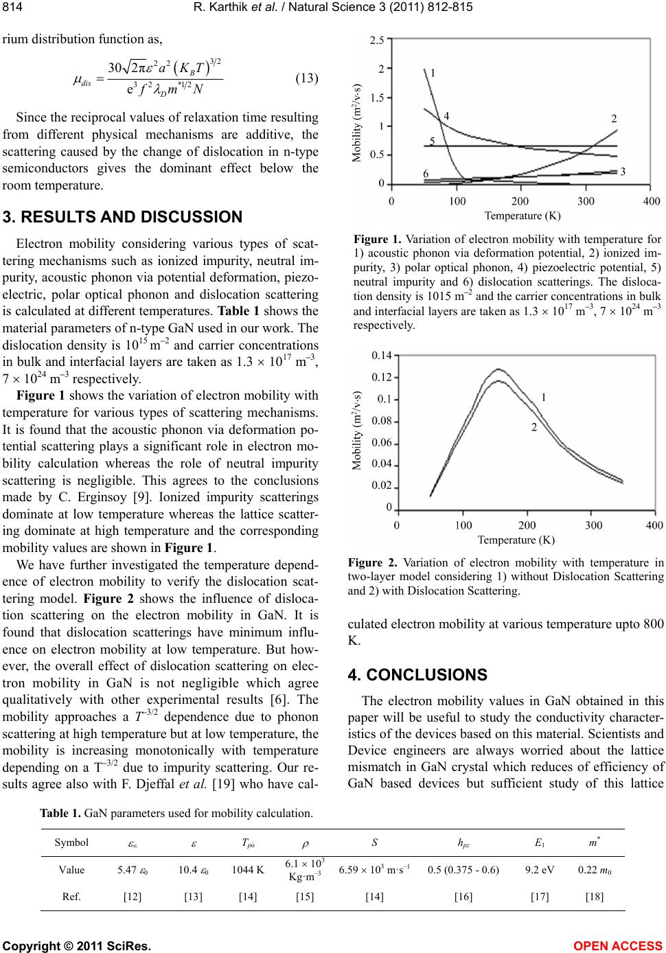 R. Karthik et al. / Natural Science 3 (2011) 812-815 Copyright © 2011 SciRes. OPEN ACCESS 814 rium distribution function as, 32 22 32 *12 30 2π e B dis D aKT fmN (13) Since the reciprocal values of relaxation time resulting from different physical mechanisms are additive, the scattering caused by the change of dislocation in n-type semiconductors gives the dominant effect below the room temperature. 3. RESULTS AND DISCUSSION Electron mobility considering various types of scat- tering mechanisms such as ionized impurity, neutral im- purity, acoustic phonon via potential deformation, piezo- electric, polar optical phonon and dislocation scattering is calculated at different temperatures. Table 1 shows the material parameters of n-type GaN used in our work. The dislocation density is 1015 m–2 and carrier concentrations in bulk and interfacial layers are taken as 1.3 1017 m–3, 7 1024 m–3 respectively. Figure 1 shows the variation of electron mobility with temperature for various types of scattering mechanisms. It is found that the acoustic phonon via deformation po- tential scattering plays a significant role in electron mo- bility calculation whereas the role of neutral impurity scattering is negligible. This agrees to the conclusions made by C. Erginsoy [9]. Ionized impurity scatterings dominate at low temperature whereas the lattice scatter- ing dominate at high temperature and the corresponding mobility values are shown in Figure 1. We have further investigated the temperature depend- ence of electron mobility to verify the dislocation scat- tering model. Figure 2 shows the influence of disloca- tion scattering on the electron mobility in GaN. It is found that dislocation scatterings have minimum influ- ence on electron mobility at low temperature. But how- ever, the overall effect of dislocation scattering on elec- tron mobility in GaN is not negligible which agree qualitatively with other experimental results [6]. The mobility approaches a T–3/2 dependence due to phonon scattering at high temperature but at low temperature, the mobility is increasing monotonically with temperature depending on a T–3/2 due to impurity scattering. Our re- sults agree also with F. Djeffal et al. [19] who have cal- Figure 1. Variation of electron mobility with temperature for 1) acoustic phonon via deformation potential, 2) ionized im- purity, 3) polar optical phonon, 4) piezoelectric potential, 5) neutral impurity and 6) dislocation scatterings. The disloca- tion density is 1015 m–2 and the carrier concentrations in bulk and interfacial layers are taken as 1.3 1017 m–3, 7 1024 m–3 respectively. Figure 2. Variation of electron mobility with temperature in two-layer model considering 1) without Dislocation Scattering and 2) with Dislocation Scattering. culated electron mobility at various temperature upto 800 K. 4. CONCLUSIONS The electron mobility values in GaN obtained in this paper will be useful to study the conductivity character- istics of the devices based on this material. Scientists and Device engineers are always worried about the lattice mismatch in GaN crystal which reduces of efficiency of GaN based devices but sufficient study of this lattice Table 1. GaN parameters used for mobility calculation. Symbol Tpo S hpz E 1 m* Value 5.47 0 10.4 0 1044 K6.1 103 Kg·m–3 6.59 103 m·s–1 0.5 (0.375 - 0.6) 9.2 eV 0.22 m0 Ref. [12] [13] [14] [15] [14] [16] [17] [18]  R. Karthik et al. / Natural Science 3 (2011) 812-815 Copyright © 2011 SciRes. OPEN ACCESS 815 mismatch and the consequence of these studies can help them to obtain an accurate theoretical model. REFERENCES [1] Jain, S.C., Willander, M., Narayan, J. and Van Over- straeten, R. (2000) III-nitride: Growth, characterization and properties. Journal of Applied Physics, 87, 965. doi:10.1063/1.371971 [2] Nakamura, S., Pearton, S.J. and Fasal, G. (2000) The blue LASER diodes. Springer, Berlin. [3] Look, D.C. and Sizelove, J.R. (1999) Dislocation Scat- tering in GaN. Physical Review Letter, 82, 1237. doi:10.1103/PhysRevLett.82.1237 [4] Dutikrushna, P., Sarkar, C.K., Mukhopadhyay, D. and Mallick, P.S. (2005) Hot electron microwave incremental conductivity of GaN. Journal of Optics, 34, 172-175. [5] Hosein, E. (2009) The effect of hydrostati pressure on material parameters and electrical transport properties in bulk GaN. Physics Letters A, 373, 1773-1776. doi:10.1016/j.physleta.2009.03.013 [6] Ng, H.M., Doppalapudi, D., Moustakas, T.D., Weimann, N.G. and Eastman, L.F. (1998) The role of dislocation scattering in n type GaN films. Applied Physical Letters, 73, 821. doi:10.1063/1.122012 [7] Weimann, N.G., Eastman, L.F., Doppalapudi, D., Ng, H.M. and Moustakas, T.D. (1998) Scattering of electrons at threading dislocations in GaN. Journal of Applied Physics, 83, 3656. doi:10.1063/1.366585 [8] Dhar, S. and Ghosh, S. (1999) Low field electron mobil- ity in GaN. Journal of Applied Physics, 86, 2668. doi:10.1063/1.371108 [9] Erginsoy, C. (1950) Neutral impurity scattering in semi- conductors. Physical Review, 79, 1013. doi:10.1103/PhysRev.79.1013 [10] Nag, B.R. (1980), Electron transport in compound semi- conductors. Springer-Verlag, Berlin. [11] Look, D.C. (1989) Electrical characterization of GaAs materials and devices. Willey, New York. [12] Lin, M.E., Sverdiov, B.N., Strite, S., Morkoe, H. and Drakin, A.E. (1993) Refractive indices of Wurtzite and Zincblende GaN. Electronics Letters, 29, 1759. doi:10.1049/el:19931172 [13] Wang, Y.J., Kaplan, R., Ng, H.K., Doverspike, K., Gaskil, D.K., Ikedo, T., Amano, H. and Akasaki, I. (1996) Mag- neto-optical studies of GaN and GaN/AlxGa1-xN: Donor zeeman spectroscopy and two dimensional electron gas cyclotron resonance. Journal of Applied Physics, 79, 8007. doi:10.1063/1.362351 [14] Morkoc, H. (1999) Nitride Semiconductors and devices, Springer-Verlag, Heidelberg/Berlin/New York. doi:10.1007/978-3-642-58562-3 [15] Schroeder, D.K. (1990), Semiconductor material and device characterization. Wiley, New York. [16] Bykhovski, A.D., Kaminski, V.V., Shur, M.S., Chen, Q.C. and Khan, M.A. (1996) Piezoelectric effect in wurtzite n type GaN. Applied Physical Letters, 68, 818. doi:10.1063/1.116543 [17] Shan, W., Schmidt, S., Yang, X.H., Song, J.J. and Golden- berg, B. (1996) Optical properties of wurtzite GaN grown by low-pressure metalorganic chemical-vapor deposition. Journal of Applied Physics, 79, 3691. doi:10.1063/1.361200 [18] Perlin, P., Staszewska, E.L. and Suchanek, B. (1996) Determination of the effective mass of GaN from infrared reflectivity and Hall effect. Applied Physical Letters, 68, 1114. doi:10.1063/1.115730 [19] Djeffal, F., Arar, D., Lakhdar, N., Bendib, T., Dibi, Z. and Chahdi, M. (2009) An approach based on particles warm computation to study the electron mobility in wurtzite GaN. Microelectronics Journal, 40, 357-359. doi:10.1016/j.mejo.2008.07.041 |