

Paper Menu >>
Journal Menu >>
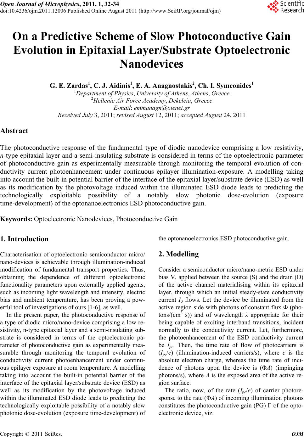 Open Journal of Microphysics, 2011, 1, 32-34 doi:10.4236/ojm.2011.12006 Published Online August 2011 (http://www.SciRP.org/journal/ojm) Copyright © 2011 SciRes. OJM On a Predictive Scheme of Slow Photoconductive Gain Evolution in Epitaxial Layer/Substrate Optoelectronic Nanodevices G. E. Zardas1, C. J. Aidinis1, E. A. Anagnostakis2, Ch. I. Symeonides1 1Department of Physics, University of Athens, Athens, Greece 2Hellenic Air Force Academy, Dekeleia, Greece E-mail: [email protected] Received July 3, 2011; revised August 12, 2011; accepted August 24, 2011 Abstract The photoconductive response of the fundamental type of diodic nanodevice comprising a low resistivity, n-type epitaxial layer and a semi-insulating substrate is considered in terms of the optoelectronic parameter of photoconductive gain as experimentally measurable through monitoring the temporal evolution of con- ductivity current photoenhancement under continuous epilayer illumination-exposure. A modelling taking into account the built-in potential barrier of the interface of the epitaxial layer/substrate device (ESD) as well as its modification by the photovoltage induced within the illuminated ESD diode leads to predicting the technologically exploitable possibility of a notably slow photonic dose-evolution (exposure time-development) of the optonanoelectronics ESD photoconductive gain. Keywords: Optoelectronic Nanodevices, Photoconductive Gain 1. Introduction Characterisation of optoelectronic semiconductor micro/ nano-devices is achievable through illumination-induced modification of fundamental transport properties. Thus, obtaining the dependence of different optoelectronic functionality parameters upon externally applied agents, such as incoming light wavelength and intensity, electric bias and ambient temperature, has been proving a pow- erful tool of investigations of ours [1-6], as well. In the present paper, the photoconductive response of a type of diodic micro/nano-device comprising a low re- sistivity, n-type epitaxial layer and a semi-insulating sub- strate is considered in terms of the optoelectronic pa- rameter of photoconductive gain as experimentally mea- surable through monitoring the temporal evolution of conductivity current photoenhancement under continu- ous epilayer exposure at room temperature. A modelling taking into account the built-in potential barrier of the interface of the epitaxial layer/substrate device (ESD) as well as its modification by the photovoltage induced within the illuminated ESD diode leads to predicting the technologically exploitable possibility of a notably slow photonic dose-evolution (exposure time-development) of the optonanoelectronics ESD photoconductive gain. 2. Modelling Consider a semiconductor micro/nano-metric ESD under bias V, applied between the source (S) and the drain (D) of the active channel materialising within its epitaxial layer, through which an initial steady-state conductivity current I0 flows. Let the device be illuminated from the active region side with photons of constant flux Φ (pho- tons/(cm2 s)) and of wavelength λ appropriate for their being capable of exciting interband transitions, incident normally to the conductivity current. Let, furthermore, the photoenhancement of the ESD conductivity current be Ipe. Then, the time rate of flow of photocarriers is (Ipe/e) (illumination-induced carriers/s), where e is the absolute electron charge, whereas the time rate of inci- dence of photons upon the device is (ΦA) (impinging photons/s), where A is the exposed area of the active re- gion surface. The ratio, now, of the rate (Ipe/e) of carrier photore- sponse to the rate (ΦA) of incoming illumination photons constitutes the photoconductive gain (PG) Γ of the opto- electronic device, viz. 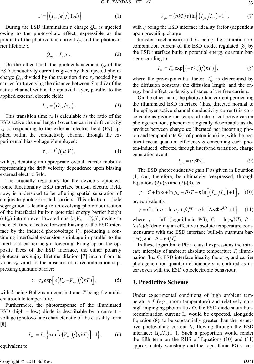 G. E. ZARDAS ET AL. 33 pe I eA . (1) During the ESD illumination a charge Qpe is injected owing to the photovoltaic effect, expressible as the product of the photovoltaic current Ipv and the photocar- rier lifetime τ, p epv QI . (2) On the other hand, the photoenhancement Ipe of the ESD conductivity current is given by this injected photo- charge Qpe divided by the transition time τtr needed by a carrier for traversing the distance between S and D of the active channel within the epitaxial layer, parallel to the applied external electric field: p epetr IQ . (3) This transition time τtr is calculable as the ratio of the ESD active channel length l over the carrier drift velocity vd corresponding to the external electric field (V/l) ap- plied within the conductivity channel through the ex- perimental bias voltage V employed: 2 tr d I V , (4) with μd denoting an appropriate overall carrier mobility representing the drift velocity dependence upon biasing external electric field. The crucially regulatory for the device’s optoelec- tronic functionality ESD interface built-in electric field, now, is understood to be offering spatial separation of conjugate photogenerated carriers. This electron – hole segregation is leading to an evolving photomodification of the interfacial built-in potential energy barrier height (eVbi) into an ever lowered one [e(Vbi – Vpv)], owing to the each time effective forward biasing of the ESD inter- face by the induced photovoltage Vpv producing a con- tinuing interfacial extension shrinkage in parallel to the interfacial barrier height lowering. Piling up on the op- posite faces of the ESD interface, the either polarity photocarriers enjoy lifetime dilation [7] into τ from its value τ0 valid in the absence of a recombination-sup- pressing quantum barrier: 0exp bi pv eV VkT , (5) with k being Boltzmann constant and T being the ambi- ent absolute temperature. Furthermore, the photoresponse of the illuminated ESD (high – low) diode is describable by a current – voltage (photovoltaic) characteristic of the causality form [8]: exp 1 pv srpv IIeV kT , (6) equivalent to ln 1 pvpv sr VkTeII , (7) with η being the ESD interface ideality factor (dependent upon prevailing charge transfer mechanism) and Isr being the saturation re- combination current of the ESD diode, regulated [8] by the ESD interface built-in potential energy quantum bar- rier according to exp sr srbi I IeVk T , (8) where the pre-exponential factor s r I is determined by the diffusion constant, the diffusion length, and the en- ergy band effective density of states of the free carriers. On the other hand, the photovoltaic current permeating the illuminated ESD interface (thus, directed normal to the epilayer active channel conductivity current) is con- ceivable as giving the temporal rate of collective carrier photogeneration, phenomenologically describable as the product between charge αe liberated per incoming pho- ton and temporal rate ΦA of photon intaking, with the per- tinent mean quantum efficiency α concerning each pho- ton-induced, effected through interband transition, charge generation event: pv I eA . (9) The ESD photoconductive gain Γ as given in Equation (1) can, therefore, be ultimately reexpressed, through Equations (2)-(5) and (7)-(9), as ln lnln1 dpv CTI sr I , (10) or, equivalently, ln lnln1 T d CT e , (11) where γ = lnΓ (logarithmic PG), C = ln(τ0V/l), β = (eVbi)/k (denoting an effective absolute temperature com- mensurate with the ESD interface built-in quantum bar- rier), and s r eA I . In these logarithmic PG γ causal expressions the intri- cate interplay of ambient absolute temperature T, illumi- nation flux Φ, ESD interface ideality factor η, and carrier photogeneration quantum efficiency α is codified as in- terwoven with the ESD optoelectronic behaviour. 3. Predictive Scheme Under experimental conditions of high ambient tem- perature T (e.g., room temperature) and relatively non- high impinging photon flux Φ, the ESD diode saturation- recombination current Isr would be expected, alongside Equation (8), to be substantially greater than the respec- tive photovoltaic current Ipv flowing through the ESD interface: (Ipv/Isr) 1. Such a proportion would render the fifth term on the RHS of Equations (10) and (11) approximately vanishing and the logarithmic PG γ cau- Copyright © 2011 SciRes. OJM 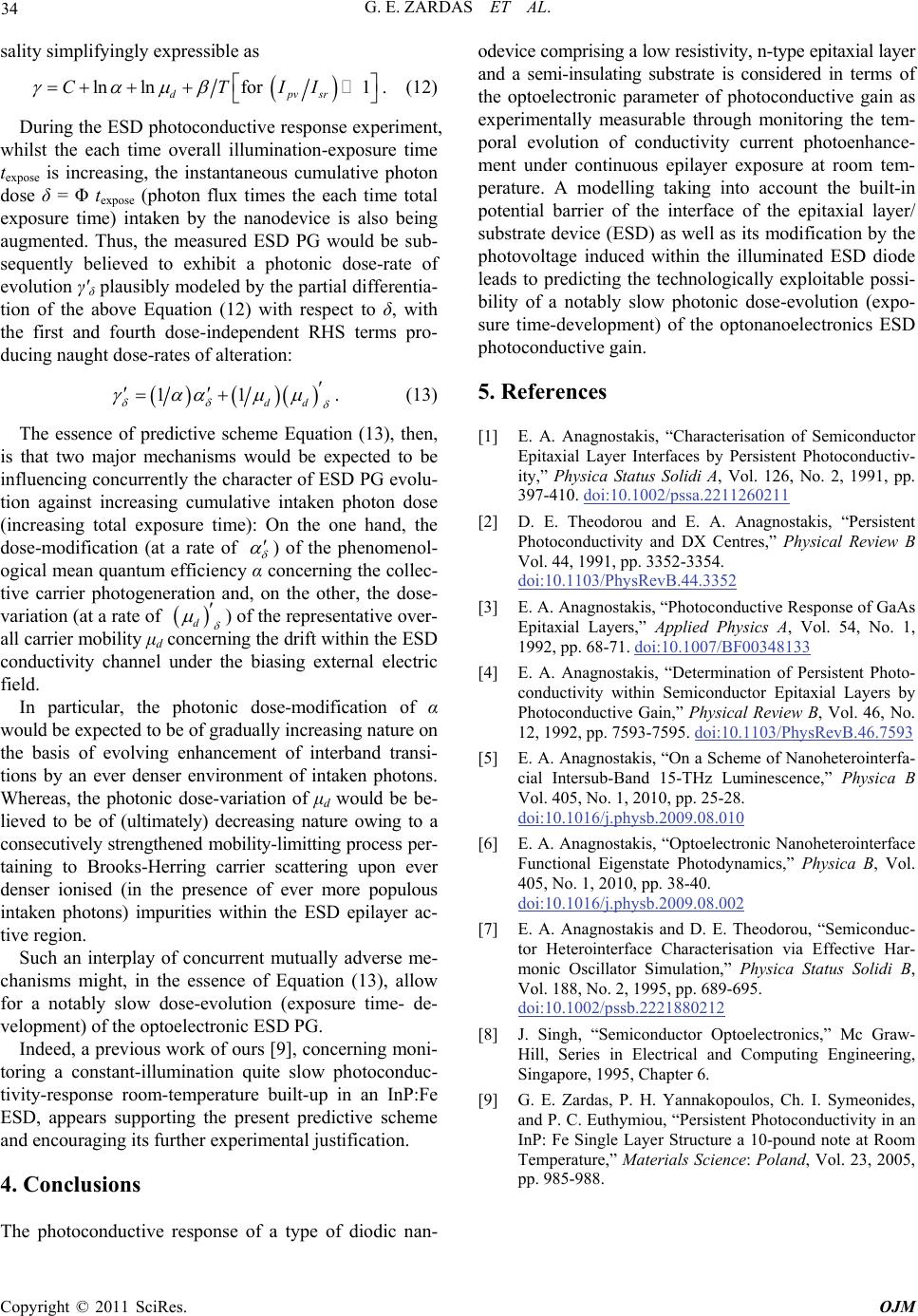 G. E. ZARDAS ET AL. Copyright © 2011 SciRes. OJM 34 sality simplifyingly expressible as lnlnfor 1 dpvsr CTII . (12) During the ESD photoconductive response experiment, whilst the each time overall illumination-exposure time texpose is increasing, the instantaneous cumulative photon dose δ = Φ texpose (photon flux times the each time total exposure time) intaken by the nanodevice is also being augmented. Thus, the measured ESD PG would be sub- sequently believed to exhibit a photonic dose-rate of evolution γ'δ plausibly modeled by the partial differentia- tion of the above Equation (12) with respect to δ, with the first and fourth dose-independent RHS terms pro- ducing naught dose-rates of alteration: 11 dd . (13) The essence of predictive scheme Equation (13), then, is that two major mechanisms would be expected to be influencing concurrently the character of ESD PG evolu- tion against increasing cumulative intaken photon dose (increasing total exposure time): On the one hand, the dose-modification (at a rate of ) of the phenomenol- ogical mean quantum efficiency α concerning the collec- tive carrier photogeneration and, on the other, the dose- variation (at a rate of d ) of the representative over- all carrier mobility μd concerning the drift within the ESD conductivity channel under the biasing external electric field. In particular, the photonic dose-modification of α would be expected to be of gradually increasing nature on the basis of evolving enhancement of interband transi- tions by an ever denser environment of intaken photons. Whereas, the photonic dose-variation of μd would be be- lieved to be of (ultimately) decreasing nature owing to a consecutively strengthened mobility-limitting process per- taining to Brooks-Herring carrier scattering upon ever denser ionised (in the presence of ever more populous intaken photons) impurities within the ESD epilayer ac- tive region. Such an interplay of concurrent mutually adverse me- chanisms might, in the essence of Equation (13), allow for a notably slow dose-evolution (exposure time- de- velopment) of the optoelectronic ESD PG. Indeed, a previous work of ours [9], concerning moni- toring a constant-illumination quite slow photoconduc- tivity-response room-temperature built-up in an InP:Fe ESD, appears supporting the present predictive scheme and encouraging its further experimental justification. 4. Conclusions he photoconductive response of a type of diodic nan- odevice comprising a low resistivity, n-type epitaxial layer and a semi-insulating substrate is considered in terms of the optoelectronic parameter of photoconductive gain as experimentally measurable through monitoring the tem- poral evolution of conductivity current photoenhance- ment under continuous epilayer exposure at room tem- perature. A modelling taking into account the built-in potential barrier of the interface of the epitaxial layer/ substrate device (ESD) as well as its modification by the photovoltage induced within the illuminated ESD diode leads to predicting the technologically exploitable possi- bility of a notably slow photonic dose-evolution (expo- sure time-development) of the optonanoelectronics ESD photoconductive gain. 5. References [1] E. A. Anagnostakis, “Characterisation of Semiconductor Epitaxial Layer Interfaces by Persistent Photoconductiv- ity,” Physica Status Solidi A, Vol. 126, No. 2, 1991, pp. 397-410. doi:10.1002/pssa.2211260211 [2] D. E. Theodorou and E. A. Anagnostakis, “Persistent Photoconductivity and DX Centres,” Physical Review B Vol. 44, 1991, pp. 3352-3354. doi:10.1103/PhysRevB.44.3352 [3] E. A. Anagnostakis, “Photoconductive Response of GaAs Epitaxial Layers,” Applied Physics A, Vol. 54, No. 1, 1992, pp. 68-71. doi:10.1007/BF00348133 [4] E. A. Anagnostakis, “Determination of Persistent Photo- conductivity within Semiconductor Epitaxial Layers by Photoconductive Gain,” Physical Review B, Vol. 46, No. 12, 1992, pp. 7593-7595. doi:10.1103/PhysRevB.46.7593 [5] E. A. Anagnostakis, “On a Scheme of Nanoheterointerfa- cial Intersub-Band 15-THz Luminescence,” Physica B Vol. 405, No. 1, 2010, pp. 25-28. doi:10.1016/j.physb.2009.08.010 [6] E. A. Anagnostakis, “Optoelectronic Nanoheterointerface Functional Eigenstate Photodynamics,” Physica B, Vol. 405, No. 1, 2010, pp. 38-40. doi:10.1016/j.physb.2009.08.002 [7] E. A. Anagnostakis and D. E. Theodorou, “Semiconduc- tor Heterointerface Characterisation via Effective Har- monic Oscillator Simulation,” Physica Status Solidi B, Vol. 188, No. 2, 1995, pp. 689-695. doi:10.1002/pssb.2221880212 [8] J. Singh, “Semiconductor Optoelectronics,” Mc Graw- Hill, Series in Electrical and Computing Engineering, Singapore, 1995, Chapter 6. [9] G. E. Zardas, P. H. Yannakopoulos, Ch. I. Symeonides, and P. C. Euthymiou, “Persistent Photoconductivity in an InP: Fe Single Layer Structure a 10-pound note at Room Temperature,” Materials Science: Poland, Vol. 23, 2005, pp. 985-988. T |