

Paper Menu >>
Journal Menu >>
 Wireless Sensor Network, 2011, 3, 300-305 doi:10.4236/wsn.2011.38031 Published Online August 2011 (http://www.SciRP.org/journal/wsn) Copyright © 2011 SciRes. WSN Characterization Process of MOSFET with Virtual Instrumentation for DP4T RF Switch—A Review Viranjay M. Srivastava1, K. S. Yadav2, G. Singh1 1Department of Electronics and Communication Engineering, Jaypee University of Information Technology, Solan, Indi a 2VLSI Design Group, Central Electro nics Engineering Research Institute (CEERI), Pilani, India E-mail: [email protected] Received June 26, 2011; revised July 22, 2011; accepted July 31, 2011 Abstract With the increasing interest in radio frequency switch by using the CMOS circuit technology for the wireless communication systems is in demand. A traditional n-MOS Single-Pole Double-Throw (SPDT) switch has good performances but only for a single operating frequency. For multiple operating frequencies, to trans- mitting or receiving information through the multiple antennas systems, known as MIMO system, a new RF switch is required which should be capable of operating with multiple antennas and frequencies as well as minimizing signal distortions and power consumption. We already have proposed a Double-Pole Four-Throw (DP4T) RF switch and in this research article we are discussing a process for the characterization of the MOSFET with Virtual Instrumentation. The procedure to characterize oxide and conductor layers that are grown or deposited on semiconductors is by studying the characteristics of a MOS capacitor that is formed of the conductor (Metal)-insulator-semiconductor layers for the purpose of RF CMOS as a switch is presented. For a capacitor formed of Metal-silicon dioxide-silicon layers with a thick oxide measured optically. Some of the calculated material parameters are away from the expected values. These errors might be due to sev- eral factors such as a possible offset capacitance of the probes due to improper contact with the wafer which is measured by using the LCR (Inductance-Capacitance-Resistance) meter with the help of Visual Engineer- ing Environment Programming (VEE Pro, a Agilent product). Keywords: RF CMOS, LCR Meter, VEE Pro, Resistance of MOSFET, DP4T Switch, RF Switch, VLSI 1. Introduction Currently, instruments as well as instrumentation tech- nique have been replaced at an increasing pace by hardware/ software mixed measurement oriented systems. The software component provides the hardware extended measuring capabilities and the instruments are thus named virtual instruments [1]. With its growth and wide applications, virtualization has come through a revival in computer system community. Virtualization offers a lot of benefits including flexibility, security, ease to con- figuration and management, reduction of cost and so forth, but at the same time it also brings a certain degree of performance overhead. Furthermore, Virtual Machine Monitor (VMM) is the core component of virtual ma- chine (VM) system and its effectiveness greatly impacts the performance of complete system [2]. Designed for measurement precision, we use LCR meters which is suitable for production applications as well as research and development purpose. As shown in Figure 1, this offers excellent performance at an affordable cost [3-5]. It has the properties of wide selection of frequency range from few Hz to 3 GHz, frequency list sweep for con- tinuous testing at multiple frequency points used for general purpose testing of surface-mount components, leaded components, materials, general purpose interface bus (GPIB) and handler interface for easy test automa- tion in production environment with 0.05% basic accu- racy. By this device we can measure the parameters as impedance (Z), admittance (Y), θ, resistance (R), Induc- tance (L), capacitance (C), transconductance (X), mag- netc field ( B), quality factor (Q), DC resistance (Rdc), DC currnt (Idc), DC voltage (Vdc) [6,7]. This LCR meter supports the VEE programming en- vironment, which provides simulated signal sources and displays. We can experiment with program flow and data 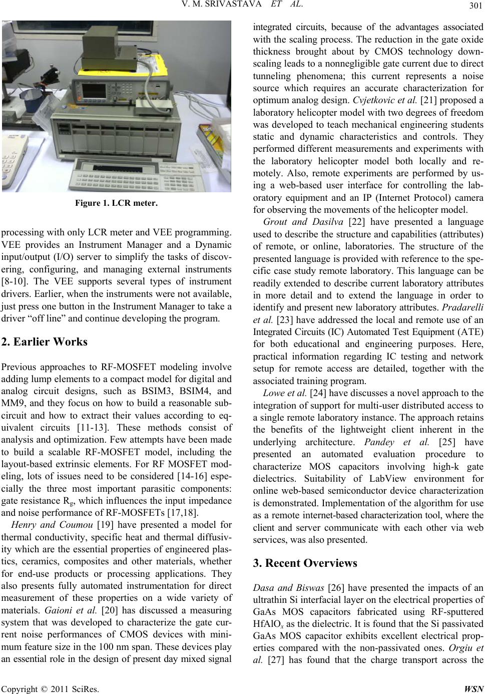 V. M. SRIVASTAVA ET AL. 301 Figure 1. LCR meter. processing with only LCR meter and VEE programming. VEE provides an Instrument Manager and a Dynamic input/output (I/O) server to simplify the tasks of discov- ering, configuring, and managing external instruments [8-10]. The VEE supports several types of instrument drivers. Earlier, when the instruments were not available, just press one button in the Instrument Manager to take a driver “off line” and continue developing the program. 2. Earlier Works Previous approaches to RF-MOSFET modeling involve adding lump elements to a compact model for digital and analog circuit designs, such as BSIM3, BSIM4, and MM9, and they focus on how to build a reasonable sub- circuit and how to extract their values according to eq- uivalent circuits [11-13]. These methods consist of analysis and optimization. Few attempts have been made to build a scalable RF-MOSFET model, including the layout-based extrinsic elements. For RF MOSFET mod- eling, lots of issues need to be considered [14-16] espe- cially the three most important parasitic components: gate resistance Rg, which influences the input impedance and noise performance of RF-MOSFETs [17,18]. Henry and Coumou [19] have presented a model for thermal conductivity, specific heat and thermal diffusiv- ity which are the essential properties of engineered plas- tics, ceramics, composites and other materials, whether for end-use products or processing applications. They also presents fully automated instrumentation for direct measurement of these properties on a wide variety of materials. Gaioni et al. [20] has discussed a measuring system that was developed to characterize the gate cur- rent noise performances of CMOS devices with mini- mum feature size in the 100 nm span. These devices play an essential role in the design of present day mixed signal integrated circuits, because of the advantages associated with the scaling process. The reduction in the gate oxide thickness brought about by CMOS technology down- scaling leads to a nonnegligible gate current due to direct tunneling phenomena; this current represents a noise source which requires an accurate characterization for optimum analog design. Cvjetkovic et al. [21] proposed a laboratory helicopter model with two degrees of freedom was developed to teach mechanical engineering students static and dynamic characteristics and controls. They performed different measurements and experiments with the laboratory helicopter model both locally and re- motely. Also, remote experiments are performed by us- ing a web-based user interface for controlling the lab- oratory equipment and an IP (Internet Protocol) camera for observing the movements of the helicopter model. Grout and Dasilva [22] have presented a language used to describe the structure and capabilities (attributes) of remote, or online, laboratories. The structure of the presented language is provided with reference to the spe- cific case study remote laboratory. This language can be readily extended to describe current laboratory attributes in more detail and to extend the language in order to identify and present new laboratory attributes. Pradarelli et al. [23] have addressed the local and remote use of an Integrated Circuits (IC) Automated Test Equipment (ATE) for both educational and engineering purposes. Here, practical information regarding IC testing and network setup for remote access are detailed, together with the associated training program. Lowe et al. [24] have discusses a novel approach to the integration of support for multi-user distributed access to a single remote laboratory instance. The approach retains the benefits of the lightweight client inherent in the underlying architecture. Pandey et al. [25] have presented an automated evaluation procedure to characterize MOS capacitors involving high-k gate dielectrics. Suitability of LabView environment for online web-based semiconductor device characterization is demonstrated. Implementation of the algorithm for use as a remote internet-based characterization tool, where the client and server communicate with each other via web services, was also presented. 3. Recent Overviews Dasa and Biswas [26] have presented the impacts of an ultrathin Si interfacial layer on the electrical properties of GaAs MOS capacitors fabricated using RF-sputtered HfAlOx as the dielectric. It is found that the Si passivated GaAs MOS capacitor exhibits excellent electrical prop- erties compared with the non-passivated ones. Orgiu et al. [27] has found that the charge transport across the Copyright © 2011 SciRes. WSN 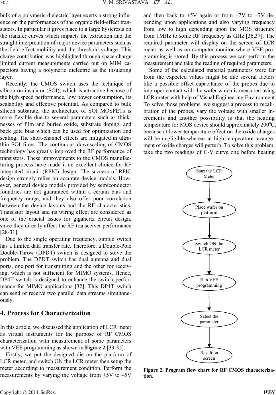 302 V. M. SRIVASTAVA ET AL. bulk of a polymeric dielectric layer exerts a strong influ- ence on the performances of the organic field-effect tran- sistors. In particular it gives place to a large hysteresis on the transfer curves which impacts the extraction and the straight interpretation of major device parameters such as the field-effect mobility and the threshold voltage. This charge contribution was highlighted through space-charge limited current measurements carried out on MIM ca- pacitors having a polymeric dielectric as the insulating layer. Recently, the CMOS switch uses the technique of silicon-on-insulator (SOI), which is attractive because of the high speed performance, low power consumption, its scalability and effective potential. As compared to bulk silicon substrate, the architecture of SOI MOSFETs is more flexible due to several parameters such as thick- nesses of film and buried oxide, substrate doping, and back gate bias which can be used for optimization and scaling. The short-channel effects are mitigated in ultra- thin SOI films. The continuous downscaling of CMOS technology has greatly improved the RF performance of transistors. These improvements to the CMOS manufac- turing process have made it an excellent choice for RF integrated circuit (RFIC) design. The success of RFIC design strongly relies on accurate device models. How- ever, general device models provided by semiconductor foundries are not guaranteed within a certain bias and frequency range, and they also offer poor correlation between the device layouts and the RF characteristics. Transistor layout and its wiring effect are considered as one of the crucial issues for gigahertz circuit design, since they directly affect the RF transceiver performance [28-31]. Due to the single operating frequency, simple switch has a limited data transfer rate. Therefore, a Double-Pole Double-Throw (DPDT) switch is designed to solve the problem. The DPDT switch has dual antenna and dual ports, one port for transmitting and the other for receiv- ing, which is not sufficient for MIMO systems. Hence, DP4T switch is designed to enhance the switch perfor- mance for MIMO applications [32]. This DP4T switch can send or receive two parallel data streams simultane- ously. 4. Process for Characterization In this article, we discussed the application of LCR meter as virtual instruments for the purpose of RF CMOS characterization with measurement of some parameters with VEE programming as shown in Figure 2 [33-35]. Firstly, we put the designed die on the platform of LCR meter, and switch ON the LCR meter then setup the meter according to measurement condition. Perform the measurements by varying the voltage from +5V to –5V and then back to +5V again or from +7V to –7V de- pending upon applications and also varying frequency from low to high depending upon the MOS structure from 1MHz to some RF frequency as GHz [36,37]. The required parameter will display on the screen of LCR meter as well as on computer monitor where VEE pro- gramming is stored. By this process we can perform the measurement and take the reading of required parameters. Some of the calculated material parameters were far from the expected values might be due several factors like a possible offset capacitance of the probes due to improper contact with the wafer which is measured using LCR meter with help of Visual Engineering Environment. To solve those problems, we suggest a process to recali- bration of the probes, vary the voltage with smaller in- crements and another possibility is that the heating temperature for MOS device should approximately 200oC, because at lower temperature effect on the oxide charges will be negligible whereas at high temperature arrange- ment of oxide charges will perturb. To solve this problem, take the two readings of C-V curve one before heating Start the LCR Meter Place wafer on p latfor m Switch ON the LCR meter Run VEE p rogramming Select the parameter Result on screen Figure 2. Program flow chart for RF CMOS characteriza- tion. Copyright © 2011 SciRes. WSN  V. M. SRIVASTAVA ET AL. 303 . 381-386. the device and other reading after heating, so that we can avoid the dislocation of charges. Also probes could have internal capacitances of their own that has not been ac- counted in the software of the machine, so the machine would actually be reading the series equivalent capaci- tance of its probes and the wafer capacitors. To solve that problem, the machine should be calibrated using refer- ence wafers whose properties are well known. 5. Conclusions Based on virtual instrumentation characterization of a RF CMOS, a capacitor which resulted in erroneous values of material parameters, mainly the substrate dopant concen- tration, on which most of the other parameters are based, we recognized those errors and correct that with a test wafer measurement for the different parameters. A RF CMOS has the properties as fixed tuned match- ing networks, low Q matching networks, ruggedness, high power output, mounting flange packages, and Sili- con grease. Power gain (a measure of power amplifica- tion, is the ratio of output power to input power, dB), Noise figure (a measure of the amount of noise added during normal operation, is the ratio of the signal-to- noise ratio at the input and the signal-to-noise ratio at the output, dB), High power dissipation (a measure of total power consumption, W or mW). Most of these parame- ters can be measured using the processes as in Figure 2. Some bipolar RF CMOS transistors are suitable for auto- motive, commercial or general industrial applications. We can calculate the drain current, resistance, poten- tial barrier, gate voltage and control voltage. After the characterization, we apply the device for the application of DP4T switches [32]. We can also apply this charac- terization process for the double-gate MOSFET and Surrounding-gate MOSFET [23,38]. Radiation characteristics and clinical implementation of an implantable MOSFET radiation detector (dosimeter) can be discussed with the proposed process. The dosime- ter is powered by radio frequency telemetry eliminating the need for a power source inside the dosimeter. The data can be accessed telemetrically for each treatment day during the course of therapy. The detector has been validated in vitro to confirm its accuracy. Variance be- tween predicted and measured dose in patients is dis- cussed. Factors such as patient setup, treatment plan er- ror, and physiologic motion can affect the accuracy of dose delivery in moving from in vitro to in vivo dose measurements [39]. A method for the extraction of dam- age metrics based upon the transient response of the drain-to-source current Ids to a step input to the gate of the device can also be performed [40]. Systematic mis- match at the drain capacitance of the IA with the current mirror load is the major contribution to a low CMRR at high frequencies. To mitigate this effect, one can use the capacitive neutralization and demonstrated its effective- ness from the fabricated CMOS instrumentation ampli- fier chip samples, achieving an average CMRR [41]. 6. References [1] O. Postolache, P. S. Girao and J. D. Pereira, “Virtual Instrumentation,” Journal of Data Modeling for Metrol ogy and Testing in Measurement Science, 2009, pp. 1-39. [2] J. H, Che, Q. M. He, Q. H. Gao and D. W. Huang, “Performance Measuring and Comparing of Virtual Machine Monitors,” Proceeding of 2008 IEEE/IFIP International Conference on Embedded and Ubiquitous Computing, 17-20 December 2008, pp [3] V. M. Srivastava, “Capacitance-Voltage Measurement for Characterization of a Metal Gate MOS Process,” Recent Trends in Engineering, Vol. 1, No. 4, May 2009, pp. 4-7. [4] S. M. Sze, “VLSI Technology,” 2nd Edition, Tata McGraw Hill, New York, 2003. [5] S. Gandhi, “VLSI Fabrication Principles, Silicon and Gallium Arsenide,” John Wiley and Sons, New York, 2002. [6] M. Popa, R. Ionel, V. Groza and M. Marcu, “Virtual In- strumentation Application for System Identification,” Pro- ceeding of IEEE Instrumentation and Measurement Tech- nology Conference, 24-27 April 2006, pp. 842-846. doi:org/10.1109/IMTC.2006.328215 [7] J. M. Thamos, “Online C-V Doping Profile Measurement of Low Dose Ion Implant,” IEEE Trans. on Electron De- vices, Vol. 27, No. 12, December 1980, pp. 2268-2273. doi:10.1109/T-ED.1980.20263 [8] M. S. Viranjay, K. S. Yadav and G. Singh, “Application of VEE Pro Software for Measurement of MOS Device Parameters Using C-V Curve,” International Journal of Computer Applications, Vol. 1, No. 7, March 2010, pp. 43-46. doi:10.5120/164-289 [9] M. S. Viranjay, K. S. Yadav and G. Singh, “Double Pole Four Throw Switch Design with CMOS Inverter,” Pro- ceding of 5th IEEE International Conference on Wireless Communication and Sensor Network, India, 15-19 De- cember 2009, pp. 1-4. doi:10.1109/WCSN.2009.5434786 [10] K. Jeyadheepan, P. Palanichamy, P. Kalyanasundaram, M. Jayaprakasam, C. Sanjeeviraja and K. Ramachandran, “Automation of Photoacoustic Spectrometer Using VEE Pro Software,” Journal of Measurement, Vol. 43, No. 10, December 2010, pp. 1336-1344. doi:10.1016/j.measurement.2010.07.011 [11] S. H. Jen, C. C. Enz and D. R. Pehlke, “Accurate Model- ing and Parameter Extraction for MOS Transistors Valid Up to 10 GHz,” IEEE Transactions Electron Devices, Vol. 46, No. 11, 1999, pp. 2217-2227. doi:10.1109/16.796299 [12] S. Lee and H. K. Yu, “A semianalytical Parameter Ex- traction of a SPICE BSIM3v3 for RF MOSFET’s Using S-Parameters,” IEEE Transition Microwave Theory and Technology, Vol. 48, No. 3, 2000, pp. 412-416. Copyright © 2011 SciRes. WSN  304 V. M. SRIVASTAVA ET AL. doi:10.1109/22.826840 [13] J. Gao and A. Werthof, “Scalable Small-Signal and Noise Modeling for Deep-Submicrometer MOSFETs,” IEEE Transaction Microwave Theory and Technology, Vol. 57, No. 4, 2009, pp. 737-744. doi:10.1109/TMTT.2009.2015075 [14] Y. Cheng, J. Deen and C. H. Chen, “MOSFET Modeling for RF IC Design,” IEEE Transaction Electron Devices, Vol. 52, No. 7, 2005, pp. 1286-1303. doi:10.1109/TED.2005.850656 [15] D. R. Pehlke, M. Schroter and A. Burstein, “High-Fre- Quency Application of MOS Compact Models and Their Development for Scalable RF Model Libraries,” Procee- ding of Custom Integrated Circuits Conference, 1998, pp. 219-222. doi:10.1109/CICC.1998.694967doi:./ .. [16] V. M. Srivastava, K. S. Yadav and G. Singh, “Analysis of Double-Gate CMOS for Double-Pole Four-Throw RF Switch Design at 45 nm Technology,” Computational Electronics, Vol. 10, No. 1-2, June 2011, pp. 229-240. doi:10.1007/s10825-011-0359-6 [17] Y. Cheng and M. Matloubian, “High Frequency Charac- terization of Gate Resistance in RF MOSFETs,” IEEE Electron Device Letters, Vol. 22, No. 2, 2001, pp. 98-100. doi:org/10.1007/s10825-011-0359-6 [18] X. Jin, J. J. Ou and C. H. Chen, “An Effective Gate Re- sistance Model for CMOS RF and Noise Modeling,” IEEE Electron Devices Meeting, Vol. 22, No. 2, 1998, pp. 961-964. doi:org/10.1109/55.902844 [19] K. Henry and K. Coumou, “New Direct Measurement Techniques for Thermal Conductivity, Thermal Diffusiv- ity, and Specific Heat of Advanced Materials,” Ther- mochimica Acta, Vol. 192, December 1991, pp. 129-134. doi:org/10.1016/0040-6031(91)87154-O [20] L. Gaioni, M. Manghisoni, L. Rattia, V. Reb, V. Spezialia and G. Traversi, “Instrumentation for Gate Current Noise Measurements on Sub-100 nm MOS Transistors,” Pro- cedingof Topical Workshop on Electronics for Particle Physics, Greece, Vol. 192, No. 12, 15-19, September 2008, pp. 436-440. [21] V. M. Cvjetkovic, M. S. Matijevic, M. D. Grujovic and M. Z. Stefanovi, “Helicopter Laboratory Model Experi- ment with Web Access,” International Journals of On- line Engineering, Vol. 5, No. 1, 2009, pp. 148-153. [22] A. Grout and R. D. Silva, “Remote Laboratory Description Language Based on XML,” Online Engineering, Vol. 5, No. 1, 2009, p. 25. [23] B. Pradarelli, L. Latorre and P. Nouet, “Integrated Circuits Testing: Remote Access to Test Equipment for Labs and Engineering,” International Journals of Online Engineering, Vol. 5, No. 1, 2009, pp. 43-50. [24] David Lowe, Chris Berry, Steve Murray, and Euan Lindsay, “Adapting a Remote Laboratory Architecture to Support Collaboration and Supervision,” International Journals of Online Engineering, Vol. 5, No. SI-1, 2009, pp. 51-56. [25] S. C. Pandey, A. Maiti, T. K. Maiti and C. K. Maiti, “Online MOS Capacitor Characterization in LabVIEW Environ- ment,” International Journals of Online Engineering, Vol. 5, No. 1, 2009, pp. 57-60. [26] P. S. Dasa and A. Biswas, “Improved Electrical and In- terfacial Properties of RF Sputtered HfAlOx on N-GaAs with Effective Si Passivation,” Applied Surface Science, Vol. 25, No. 6, 2010, pp. 6618-6625 doi:10.1016/j.apsusc.2010.04.058 [27] E. Orgiu, S. Locci, B. Fraboni, E. Scavetta, P. Lugli and A. Bonfiglio, “Analysis of the Hysteresis in Organic Thin-Film Transistors with Polymeric Gate Dielectric,” International Journals of Online Engineering, Vol. 12, 2011, pp. 477-485. [28] Y. N. Yu, L. L. Sun and J. Liu, “RF CMOS Modeling: A Scalable Model of RF-MOSFET with Different Numbers of Fingers,” Journal of Semiconductors, Vol. 12, No. 3, November 2010, pp. 477-485. doi:10.1088/1674-4926/31/11/114007 [29] C. Cao and K. O. Kenneth, “A 90 GHz Voltage Con- trolled Oscillator with a 2.2 GHz Tuning Range in a 130 nm CMOS Technology,” Proceeding of Sump VLSI Cir- cuits Dig Technology, 2005, p. 242. doi:10.1109/VLSIC.2005.1469376 [30] C. Y. Chan, S. C. Chen and M. H.Tsai, “Wiring Effect Optimization in 65 nm Low-Power NMOS,” IEEE Elec- tron Device Letters, Vol. 29, No. 11, 2008, p. 1245. doi:10.1109/LED.2008.2005515 [31] V. M. Srivastava, K. S. Yadav and G. Singh, “Design and performance Analysis of Double-Gate MOSFET Over Single-Gate MOSFET for RF Switch,” Microelectronics Journals, Vol. 42, No. 3, March 2011, pp. 527-534. doi:10.1016/j.mejo.2010.12.007 [32] M. S.Viranjay, K. S. Yadav and G. Singh, “Performance of Double-Pole Four-Throw Double-Gate RF CMOS Switch in 45-nm Technology,”International Journals of Wireless Engineering and Technology, Vol. 1, No. 2, Octorber 2010, pp. 47-54. doi:10.4236/ wet.2010.12008 [33] P. H. Woerlee, M. J. Knitel, R. Langevelde, D. Klaassen, L. F. Tiemeijer and A. J. Scholten, “RF CMOS Perform- ance Trends,” IEEE Transaction on Electron Devices, Vol. 48, No. 8, August 2001, pp. 1776-1782. doi:10.1109/16.936707 [34] K. K. Koichiand, “Numerical Analysis of Switching Characteristics in SOI MOSFET,” IEEET Transaction on Electron Devi ces, Vol. 33, February 1986, pp. 133-139. doi:10.1109/T-ED.1986.22449 [35] E. H. Nicollian and J. R. Brews, “MOS Physics and Technology,” Wiley, New York, 1982. [36] Viranjay M. Srivastava, K. S. Yadav and G. Singh, “Dou- ble-Pole Four-Throw RF CMOS Switch Design with Double-Gate Transistor,” Proceeding of 2010 Annual IEEE India Conference (INDICON-2010), 17-19 December 2010, India, pp. 1-4. doi:10.1109/INDCON.2010.5712754 [37] S. M. Sze, “Physics of Semiconductor Devices”, 2nd Edition, Wiley, New York, 1985. [38] V. M. Srivastava, K. S. Yadav and G. Singh, “Design and Performance Analysis of Cylindrical Surrounding Dou- ble-Gate MOSFET for RF Switch,” Microelectronics Journal, Vol. 42, No. 9, September 2011, pp. 1025-1036. Copyright © 2011 SciRes. WSN  V. M. SRIVASTAVA ET AL. Copyright © 2011 SciRes. WSN 305 doi:10.1016/j.mejo.2011.07.003 [39] L. J. Passmore, O. Awadelkarim and J. P. Cusumano, “High Sensitivity Tracking of MOSFET Damage Using Dynamic-Mode Transient Measurements,” IEEE Trans. on Instrumentation and Measurement, Vol. 59, No. 6, June 2010, pp. 1734-1742. doi:10.1109/TIM.2009.2028213 [40] G. P. Beyer and C. W. Scarantino, “An Implantable MOSFET Dosimeter for the Measurement of Radiation Dose in Tissue During Cancer Therapy,” IEEE Journal of Sensors, Vol. 8, No. 1, January 2008, pp. 38-51. doi:10.1109/JSEN.2007.912542 [41] A. Worapishet, A. Demosthenous and X. Liu, “A CMOS Instrumentation Amplifier with 90 dB CMRR at 2 MHz Using Capacitive Neutralization: Analysis, Design Consi- derations, and Implementation,” IEEE Transaction on Circuits and Systems, Vol. 58, No. 4, April 2011, pp. 699-710. doi:10.1109/TCSI.2010.2078850 |