

Paper Menu >>
Journal Menu >>
 Materials Sciences and Applicatio n, 2011, 2, 993-999 doi:10.4236/msa.2011.28134 Published Online August 2011 (http://www.SciRP.org/journal/msa) Copyright © 2011 SciRes. MSA 993 Investigation of Electrical Transport in PECVD Grown a-SiCx:H Thin Film Orhan Özdemir*, Kutsal Bozkurt, Kubilay Kutlu Physics Department, Yildiz Technical University, Esenler/İstanbul, Turkey. Email: *[email protected] Received April 8th, 2011; revised April 28th, 2011; accepted May 11th, 2011. ABSTRACT Dc/ac transport characteristic of PECVD grown hydrogenated amorphous silicon carbide (a-SiCx:H) thin film was in- vestigated in MIS (metal/insulator/semiconductor) structure by dc current/voltage (I/V) at different temperature (T), ac admittance vs. temperature at constant gate bias voltages and deep level transient spectroscopy (DLTS), respectively. According to I-V-T analysis, two main regimes exhibited. At low electric field, apparent Ohm’s law dominated with Arrhenius type thermal activation energy (EA) around 0.4 eV in both forward and reverse directions. At high field, on the contrary, space charge limited (SCL) current mechanism was eventual. The current transport mechanisms and its temperature/frequency dependence were interpreted by a thermally activated hopping processes across the localized states within a-SiCx:H thin film since 0.4 eV as EA was not high enough for intrinsic band conduction. Instead, transport of charge carriers took place in two steps; first a carrier is thermally excited to an empty energy level from an occupied state then multi-step tunnelling or hopping starts over. Therefore, the two steps mechanisms manifested as single acti- vation energy, differing only through capture cross sections. In turn, two steps in capacitance together with conduc- tance peaks in C-(G)-T while convoluted DLTS signal associated with such events in the measurements. Keywords: A-SiCx:H, Dc/Ac Transport, Conduction Mechanisms, Apparent Activation Energy, Admittance, DLTS, Hopping 1. Introduction Both tunability of energy band gap from 1.9 - 3.2 eV with different carbon content (x) [1] and n-/p- type dopa- bility by appropriate doping gases [1] lead an opportunity of amorphous hydrogenated silicon carbide (a-SiCx:H) films to be used in solar cell technology and light-emitti- ng diodes (LED’s). In former, owing to the excellent surface passivation of crystalline silicon (c-Si) and large area deposition capability, a-SiCx:H films are used in silicon solar cell applications. Recent works have shown that Si-rich a-SiCx:H films with low power regime pos- sesses brilliant electronic surface passivation in silicon heterojunction solar cells [2-8]. Improvement in silicon heterojunction solar cells to achieve high conversion ef- ficiency (greater than 22%) [9,10] is possible by elec- tronic surface passivation, i.e., low recombination loss of photo-generated carriers. Contrary to that LED’s applications require bipolar carrier transport and efficient recombination rate of in- jected electron-hole pairs within the intrinsic layer of a-SiCx:H films. Each phenomena, transport and/or re- combination issues, limits the efficiency of LED’s in which carriers might flow through either localized or extended states via hopping [11] in a-SiCx:H films. Within this context, since carrier injection issue and na- ture/amount of localized density of states (DOS) distri- bution are tightly bound with each other, d.c. and a.c. conductivities seem to be convenient techniques for characterizing electrical features of the a-SiCx:H film within a metal/insulator/semiconductor structure. In other words, d.c. current/voltage (I/V) at different temperatures, a.c. admittance (Y = G + jωC, G = conductance, C = ca- pacitance, and ω = frequency) versus bias voltage and/or temperature at constant gate bias voltages and deep level transient spectroscopy (DLTS) are proper techniques to employ for investigating electrical features of a-SiCx:H film in MIS structure. 2. Film Fabrication and Experimental Detail a-SiCx:H film studied in this work was grown, under the mixture of 30 ccm SiH4 (silane) and 30 ccm C2H4 (eth- ylene), by 13.56 MHz plasma enhanced chemical vapor 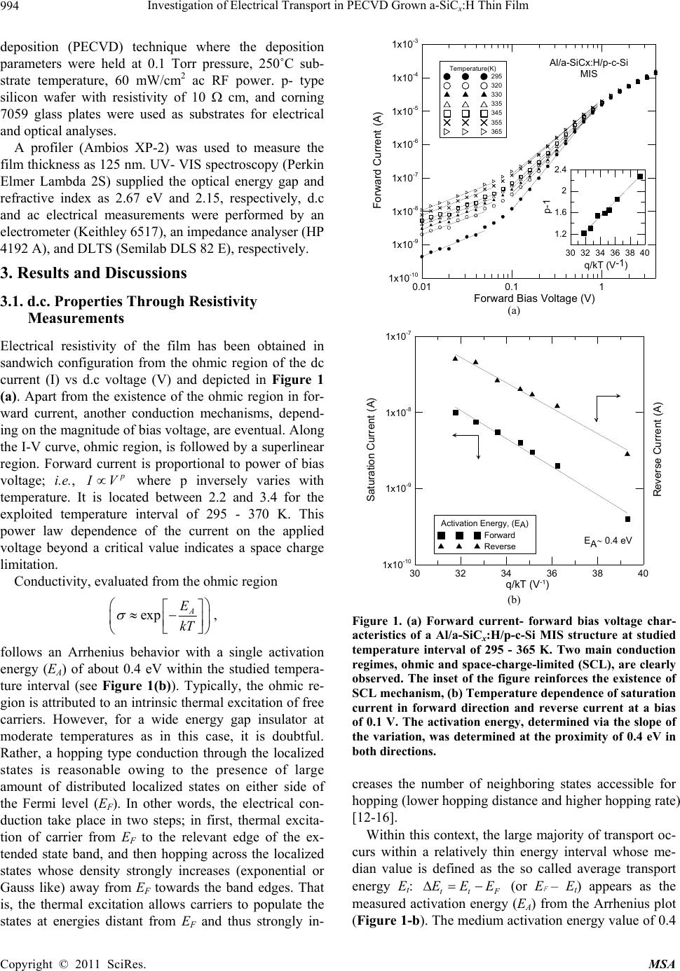 Investigation of Electrical Transport in PECVD Grown a-SiC :H Thin Film 994 x deposition (PECVD) technique where the deposition parameters were held at 0.1 Torr pressure, 250˚C sub- strate temperature, 60 mW/cm2 ac RF power. p- type silicon wafer with resistivity of 10 cm, and corning 7059 glass plates were used as substrates for electrical and optical analyses. A profiler (Ambios XP-2) was used to measure the film thickness as 125 nm. UV- VIS spectroscopy (Perkin Elmer Lambda 2S) supplied the optical energy gap and refractive index as 2.67 eV and 2.15, respectively, d.c and ac electrical measurements were performed by an electrometer (Keithley 6517), an impedance analyser (HP 4192 A), and DLTS (Semilab DLS 82 E), respectively. 3. Results and Discussions 3.1. d.c. Properties Through Resistivity Measurements Electrical resistivity of the film has been obtained in sandwich configuration from the ohmic region of the dc current (I) vs d.c voltage (V) and depicted in Figure 1 (a). Apart from the existence of the ohmic region in for- ward current, another conduction mechanisms, depend- ing on the magnitude of bias voltage, are eventual. Along the I-V curve, ohmic region, is followed by a superlinear region. Forward current is proportional to power of bias voltage; i.e., p I V where p inversely varies with temperature. It is located between 2.2 and 3.4 for the exploited temperature interval of 295 - 370 K. This power law dependence of the current on the applied voltage beyond a critical value indicates a space charge limitation. Conductivity, evaluated from the ohmic region exp A E kT , follows an Arrhenius behavior with a single activation energy (EA) of about 0.4 eV within the studied tempera- ture interval (see Figure 1(b)). Typically, the ohmic re- gion is attributed to an intrinsic thermal excitation of free carriers. However, for a wide energy gap insulator at moderate temperatures as in this case, it is doubtful. Rather, a hopping type conduction through the localized states is reasonable owing to the presence of large amount of distributed localized states on either side of the Fermi level (EF). In other words, the electrical con- duction take place in two steps; in first, thermal excita- tion of carrier from EF to the relevant edge of the ex- tended state band, and then hopping across the localized states whose density strongly increases (exponential or Gauss like) away from EF towards the band edges. That is, the thermal excitation allows carriers to populate the states at energies distant from EF and thus strongly in- 0.01 0.11 Forward Bias Voltag e (V) 1x10 -10 1x10 -9 1x10 -8 1x10 -7 1x10 -6 1x10 -5 1x10 -4 1x10 -3 Forward Curr ent ( A) Temperature(K) 295 320 330 335 345 355 365 Al/a-SiCx:H/p-c-Si MIS 30 32 34 36 38 40 q/kT (V-1) 1.2 1.6 2 2.4 p-1 (a) 30 32 34 36 38 40 q/kT (V -1 ) 1x10 -10 1x10 -9 1x10 -8 1x10 -7 Satu r at ion Cu r r ent ( A) Rev e r se Cu r r ent ( A) Activation Energy, (EA) Forward Reverse EA 0.4 eV (b) Figure 1. (a) Forward current- forward bias voltage char- acteristics of a Al/a-SiCx:H/p-c-Si MIS structure at studied temperature interval of 295 - 365 K. Two main conduction regimes, ohmic and space-charge-limited (SCL), are clearly observed. The inset of the figure reinforces the existence of SCL mechanism, (b) Temperature dependence of saturation current in forward direction and reverse current at a bias of 0.1 V. The activation energy, determined via the slope of the variation, was determined at the proximity of 0.4 eV in both directions. creases the number of neighboring states accessible for hopping (lower hopping distance and higher hopping rate) [12-16]. Within this context, the large majority of transport oc- curs within a relatively thin energy interval whose me- dian value is defined as the so called average transport energy Et: ttF EEE (or E F – Et) appears as the measured activation energy (EA) from the Arrhenius plot (Figure 1-b). The medium activation energy value of 0.4 Copyright © 2011 SciRes. MSA 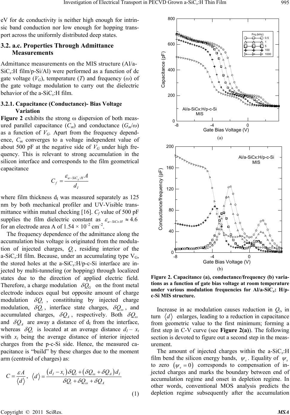 Investigation of Electrical Transport in PECVD Grown a-SiC :H Thin Film995 x eV for dc conductivity is neither high enough for intrin- sic band conduction nor low enough for hopping trans- port across the uniformly distributed deep states. 3.2. a.c. Properties Through Admittance Measurements Admittance measurements on the MIS structure (Al/a- SiCx:H film/p-Si/Al) were performed as a function of dc gate voltage (VG), temperature (T) and frequency (ω) of the gate voltage modulation to carry out the dielectric behavior of the a-SiCx:H film. 3.2.1. Capaci t ance ( Con ductance)- Bias Volt age Variation Figure 2 exhibits the strong ω dispersion of both meas- ured parallel capacitance (Cm) and conductance (Gm/ω) as a function of VG. Apart from the frequency depend- ence, Cm converges to a voltage independent value of about 500 pF at the negative side of VG under high fre- quency. This is relevant to strong accumulation in the silicon interface and corresponds to the film geometrical capacitance : x aSiCH f I A Cd where film thickness dI was measured separately as 125 nm by both mechanical profiler and UV-Visible trans- mittance within mutual checking [16]. Cf value of 500 pF supplies the film dielectric constant as :4.6 aSiCxH for an electrode area A of 1.54 × 10⁻² cm–2. The frequency dependence of the admittance along the accumulation bias voltage is originated from the modula- tion of injected charges, t, residing interior of the a-SiCx:H film. Because, under an accumulating type VG, the stored holes at the a-SiCx:H/p-c-Si interface are in- jected by multi-tunneling (or hopping) through localized states due to the direction of applied electric field. Therefore, a charge modulation G Q Q on the front metal electrode induces equal but opposite amount of charge modulation s Q , constitituing by injected charge modulation, t Q , interface state charges, s s Q , and accumulated charges, A Q , respectively. Both s s Q and A Q are away a distance of dI from the interface, whereas t Q is located at an average distance dI – xt with xt being the average distance of interior injected charges from the p-c-Si side. Hence, the measured ca- pacitance is “build” by these charges due to the moment arm (centroid of charges) as: A Cd , I ttss A tssA dxQQ Qd dQQ Q I (1) -8 -40 GateBias Voltage (V) 0 200 400 600 800 Capacitance (pF) Frq.(kHz) 0.5 1 5 100 1000 Al/a-SiCx:H/p-c-Si MIS (a) -8 -40 GateBias Voltage (V) 0 40 80 120 160 200 Conductance/f r equency (pF) Al/a-SiCx:H/p-c-Si MIS (b) Figure 2. Capacitance (a), c onductance/frequency (b) varia- tions as a function of gate bias voltage at room temperature under various modulation frequencies for Al/a-SiCx: H/p- c-Si MIS structure. Increase in ac modulation causes reduction in Qt, in turn d enlarges, leading to a reduction in capacitance from geometric value to the first minimum; forming a first step in C-V curve (see Figure 2(a)). The following section is devoted to figure out a second step in the meas- urement. The amount of injected charges within the a-SiCx:H film bend the silicon energy bands, s . Equality of s to zero 0 s corresponds to compensation of in- jected charges and marks the boundary between end of accumulation regime and onset in depletion regime. In other words, conventional MOS analysis predicts the depletion regime subsequently after the accumulation Copyright © 2011 SciRes. MSA 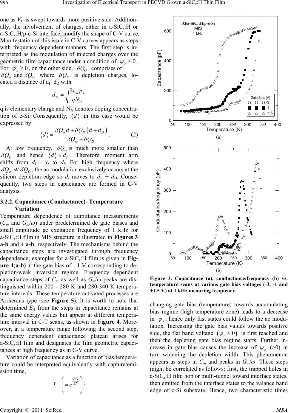 Investigation of Electrical Transport in PECVD Grown a-SiC :H Thin Film 996 x one as VG is swept towards more positive side. Addition- ally, the involvement of charges, either in a-SiCx:H or a-SiCx:H/p-c-Si interface, modify the shape of C-V curve. Manifestation of this issue in C-V curves appears as steps with frequency dependent manners. The first step is in- terpreted as the modulation of injected charges over the geometric film capacitance under a condition of 0 s . For 0 s , on the other side, G Q comprises of and s sD QQ where D Q is depletion charges, lo- cated a distance of dI+dD with 2 s is A qN D d q is elementary charge and NA denotes doping concentra- tion of c-Si. Consequently, d in this case would be expressed by ss Qd D D ss D Qd d dQQ . (2) At low frequency, s s Q is much more smaller than D Q and hence I dd. Therefore, moment arm shifts from dI – xt to dI. For high frequency where s sD QQ , the ac modulation exclusively occurs at the silicon depletion edge so dI moves to dI + dD. Conse- quently, two steps in capacitance are formed in C-V analysis. 3.2.2. Capacit ance ( Con ductance)- Temperature Variation Temperature dependence of admittance measurements (Cm and Gm/ω) under predetermined dc gate biases and small amplitude ac excitation frequency of 1 kHz for a-SiCx:H film in MIS structure is illustrated in Figures 3 a-b and 4 a-b, respectively. The mechanisms behind the capacitance steps are investigated through frequency dependence; examples for a-SiCx:H film is given in Fig- ure 4(a-b) at the gate bias of –1 V corresponding to de- pletion/weak inversion regime. Frequency dependent capacitance steps of Cm as well as Gm/ω peaks are dis- tinguished within 200 - 280 K and 280-340 K tempera- ture intervals. These temperature activated processes are Arrhenius type (see Figure 5). It is worth to note that determined EA from the steps in capacitance remains at the same energy values but appear at different tempera- ture interval in C-T scans, as shown in Figure 4. More- over, at a temperature range following the second step, frequency dependent capacitance plateau arises for a-SiCx:H film and designates the film geometric capaci- tances at high frequency as in C-V curve. Variation of capacitance as a function of bias/tempera- ture could be interpreted equivalently with capture/emi- ssion time, s q kT e : 100 200 300 400 50150 250 350 Temper ature (K) 0 200 400 600 Capacitance ( pF) Gate Bias (V) -3 -1 +1.5 1 kHz Al/a-SiCx:H/p-c-Si MIS Al/a-SiCx:H/p-c-Si (a) 100 200 300 400 50150 250 350 Tem per ature (K) 0 100 200 300 400 500 Conductance / frequency ( pF) (b) Figure 3. Capacitance (a), conductance/frequency (b) vs. temperature scans at various gate bias voltages (-3, -1 and +1.5 V) at 1 kHz meauring frequency. changing gate bias (temperature) towards accumulating bias regime (high temperature zone) leads to a decrease in s , hence only fast states could follow the ac modu- lation. Increasing the gate bias values towards positive side, the flat band voltage 0 s is first reached and then the depleting gate bias regime starts. Further in- crease in gate bias causes the increase of s (>0) in turn widening the depletion width. This phenomenon appears as steps in Cm and peaks in Gm/ω. These steps might be correlated as follows: first, the trapped holes in a-SiCx:H film hop or multi-tunnel toward interface states, then emitted from the interface states to the valance band edge of c-Si substrate. Hence, two characteristic times Copyright © 2011 SciRes. MSA 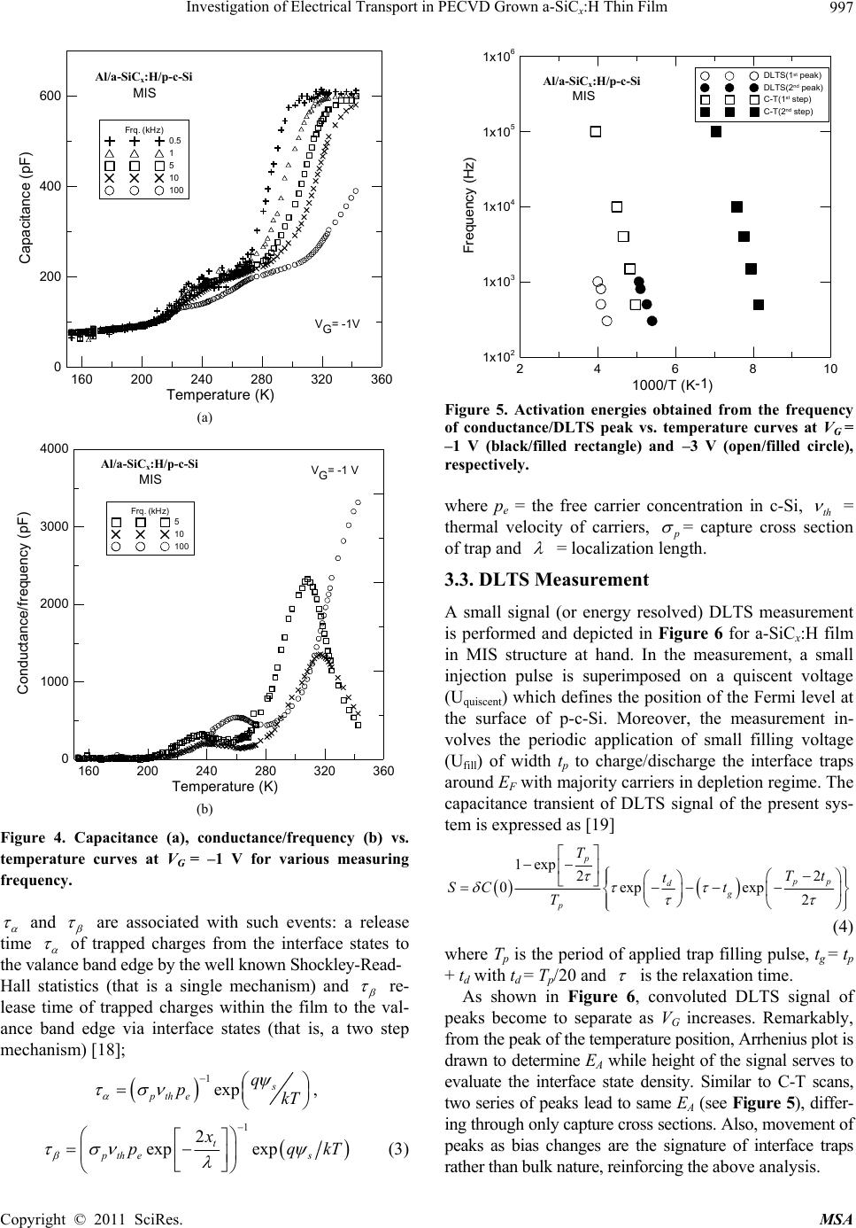 Investigation of Electrical Transport in PECVD Grown a-SiC :H Thin Film997 x 160 200 240 280 320 360 Tem pera tu re ( K) 0 200 400 600 Capacitance (pF) Frq. (kHz)0.5 1 5 10 100 Al/a-SiCx:H/p-c-Si MIS VG= -1V (a) 160200240 280 320360 Temper a t ur e (K) 0 1000 2000 3000 4000 Conductance/f requency (pF) Frq. (kHz)5 10 100 Al/a-SiCx:H/p-c-Si MIS VG= -1 V (b) Figure 4. Capacitance (a), conductance/frequency (b) vs. temperature curves at VG = –1 V for various measuring frequency. and are associated with such events: a release time of trapped charges from the interface states to the valance band edge by the well known Shockley-Read- Hall statistics (that is a single mechanism) and re- lease time of trapped charges within the film to the val- ance band edge via interface states (that is, a two step mechanism) [18]; 1exp s pth e q pkT , 1 2 exp exp t pth es x pq kT (3) 2468 1000/T (K-1) 10 1x10 2 1x10 3 1x10 4 1x10 5 1x10 6 Frequency (Hz) DLTS(1 st peak) DLTS(2 nd peak) C-T(1 st step) C-T(2 nd step) Al Al/a-SiCx:H/p-c-Si /a-SiCx:H/p-c-Si MIS Al/a-SiCx:H/p-c-Si Figure 5. Activation energies obtained from the frequency of conductance/DLTS peak vs. temperature curves at VG = –1 V (black/filled rectangle) and –3 V (open/filled circle), respectively. Al/a-SiCx:H/p-c-Si where pe = the free carrier concentration in c-Si, th = thermal velocity of carriers, p = capture cross section of trap and = localization length. 3.3. DLTS Measurement A small signal (or energy resolved) DLTS measurement is performed and depicted in Figure 6 for a-SiCx:H film in MIS structure at hand. In the measurement, a small injection pulse is superimposed on a quiscent voltage (Uquiscent) which defines the position of the Fermi level at the surface of p-c-Si. Moreover, the measurement in- volves the periodic application of small filling voltage (Ufill) of width tp to charge/discharge the interface traps around EF with majority carriers in depletion regime. The capacitance transient of DLTS signal of the present sys- tem is expressed as [19] 1exp 2 2 0expexp 2 p pp d g p T Tt t SC t T (4) where Tp is the period of applied trap filling pulse, tg = tp + td with td = Tp/20 and is the relaxation time. As shown in Figure 6, convoluted DLTS signal of peaks become to separate as VG increases. Remarkably, from the peak of the temperature position, Arrhenius plot is drawn to determine EA while height of the signal serves to evaluate the interface state density. Similar to C-T scans, two series of peaks lead to same EA (see Figure 5), differ- ing through only capture cross sections. Also, movement of peaks as bias changes are the signature of interface traps rather than bulk nature, reinforcing the above analysis. Copyright © 2011 SciRes. MSA 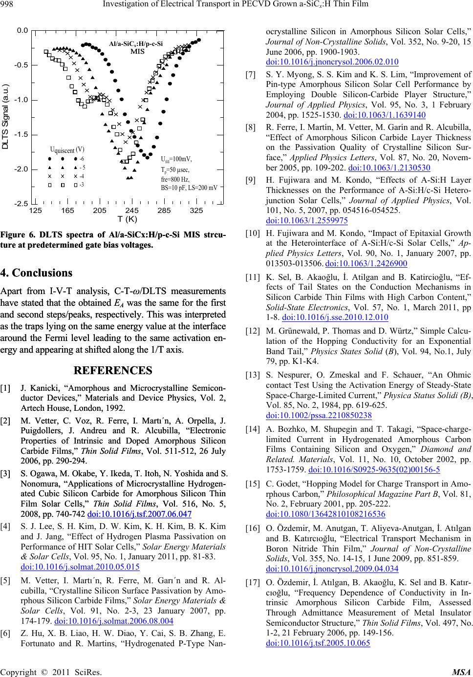 Investigation of Electrical Transport in PECVD Grown a-SiC :H Thin Film 998 x 125 165 205 245 285 325 T(K) -2.5 -2.0 -1.5 -1.0 -0.5 0.0 DLTS Signal ( a.u.) Uquiscent (V) -6 - 5 -4 -3 U fill =100mV, T p =50 sec, fre=800 Hz, BS=10 pF, LS=200 Al/a-SiCx:H/p-c-Si MIS -c-Si MIS mV Figure 6. DLTS spectra of Al/a-SiCx:H/p-c-Si MIS strcu- ture at predetermined gate bias voltages. Figure 6. DLTS spectra of Al/a-SiCx:H/p-c-Si MIS strcu- ture at predetermined gate bias voltages. 4. Conclusions 4. Conclusions Apart from I-V-T analysis, C-T-ω/DLTS measurements have stated that the obtained EA was the same for the first and second steps/peaks, respectively. This was interpreted as the traps lying on the same energy value at the interface around the Fermi level leading to the same activation en- ergy and appearing at shifted along the 1/T axis. Apart from I-V-T analysis, C-T-ω/DLTS measurements have stated that the obtained EA was the same for the first and second steps/peaks, respectively. This was interpreted as the traps lying on the same energy value at the interface around the Fermi level leading to the same activation en- ergy and appearing at shifted along the 1/T axis. REFERENCES REFERENCES [1] J. Kanicki, “Amorphous and Microcrystalline Semicon- ductor Devices,” Materials and Device Physics, Vol. 2, Artech House, London, 1992. [1] J. Kanicki, “Amorphous and Microcrystalline Semicon- ductor Devices,” Materials and Device Physics, Vol. 2, Artech House, London, 1992. [2] M. Vetter, C. Voz, R. Ferre, I. Martı´n, A. Orpella, J. Puigdollers, J. Andreu and R. Alcubilla, “Electronic Properties of Intrinsic and Doped Amorphous Silicon Carbide Films,” Thin Solid Films, Vol. 511-512, 26 July 2006, pp. 290-294. [2] M. Vetter, C. Voz, R. Ferre, I. Martı´n, A. Orpella, J. Puigdollers, J. Andreu and R. Alcubilla, “Electronic Properties of Intrinsic and Doped Amorphous Silicon Carbide Films,” Thin Solid Films, Vol. 511-512, 26 July 2006, pp. 290-294. [3] S. Ogawa, M. Okabe, Y. Ikeda, T. Itoh, N. Yoshida and S. Nonomura, “Applications of Microcrystalline Hydrogen- ated Cubic Silicon Carbide for Amorphous Silicon Thin Film Solar Cells,” Thin Solid Films, Vol. 516, No. 5, 2008, pp. 740-742 doi:10.1016/j.tsf.2007.06.047 [3] S. Ogawa, M. Okabe, Y. Ikeda, T. Itoh, N. Yoshida and S. Nonomura, “Applications of Microcrystalline Hydrogen- ated Cubic Silicon Carbide for Amorphous Silicon Thin Film Solar Cells,” Thin Solid Films, Vol. 516, No. 5, 2008, pp. 740-742 doi:10.1016/j.tsf.2007.06.047 [4] S. J. Lee, S. H. Kim, D. W. Kim, K. H. Kim, B. K. Kim and J. Jang, “Effect of Hydrogen Plasma Passivation on Performance of HIT Solar Cells,” Solar Energy Materials & Solar Cells, Vol. 95, No. 1, January 2011, pp. 81-83. doi:10.1016/j.solmat.2010.05.015 [5] M. Vetter, I. Martı´n, R. Ferre, M. Garı´n and R. Al- cubilla, “Crystalline Silicon Surface Passivation by Amo- rphous Silicon Carbide Films,” Solar Energy Materials & Solar Cells, Vol. 91, No. 2-3, 23 January 2007, pp. 174-179. doi:10.1016/j.solmat.2006.08.004 [6] Z. Hu, X. B. Liao, H. W. Diao, Y. Cai, S. B. Zhang, E. Fortunato and R. Martins, “Hydrogenated P-Type Nan- ocrystalline Silicon in Amorphous Silicon Solar Cells,” Journal of Non-Crystalline Solids, Vol. 352, No. 9-20, 15 June 2006, pp. 1900-1903. doi:10.1016/j.jnoncrysol.2006.02.010 Al/a-SiCx:H/p-c-Si [7] S. Y. Myong, S. S. Kim and K. S. Lim, “Improvement of Pin-type Amorphous Silicon Solar Cell Performance by Employing Double Silicon-Carbide Player Structure,” Journal of Applied Physics, Vol. 95, No. 3, 1 February 2004, pp. 1525-1530. doi:10.1063/1.1639140 [8] R. Ferre, I. Martín, M. Vetter, M. Garín and R. Alcubilla, “Effect of Amorphous Silicon Carbide Layer Thickness on the Passivation Quality of Crystalline Silicon Sur- face,” Applied Physics Letters, Vol. 87, No. 20, Novem- ber 2005, pp. 109-202. doi:10.1063/1.2130530 [9] H. Fujiwara and M. Kondo, “Effects of A-Si:H Layer Thicknesses on the Performance of A-Si:H/c-Si Hetero- junction Solar Cells,” Journal of Applied Physics, Vol. 101, No. 5, 2007, pp. 054516-054525. doi:10.1063/1.2559975 [10] H. Fujiwara and M. Kondo, “Impact of Epitaxial Growth at the Heterointerface of A-Si:H/c-Si Solar Cells,” Ap- plied Physics Letters, Vol. 90, No. 1, January 2007, pp. 013503-013506. doi:10.1063/1.2426900 [11] K. Sel, B. Akaoğlu, İ. Atilgan and B. Katircioğlu, “Ef- fects of Tail States on the Conduction Mechanisms in Silicon Carbide Thin Films with High Carbon Content,” Solid-State Electronics, Vol. 57, No. 1, March 2011, pp 1-8. doi:10.1016/j.sse.2010.12.010 [12] M. Grünewald, P. Thomas and D. Würtz,” Simple Calcu- lation of the Hopping Conductivity for an Exponential Band Tail,” Physics States Solid (B), Vol. 94, No.1, July 79, pp. K1-K4. [13] S. Nespurer, O. Zmeskal and F. Schauer, “An Ohmic contact Test Using the Activation Energy of Steady-State Space-Charge-Limited Current,” Physica Status Solidi (B), Vol. 85, No. 2, 1984, pp. 619-625. doi:10.1002/pssa.2210850238 [14] A. Bozhko, M. Shupegin and T. Takagi, “Space-charge- limited Current in Hydrogenated Amorphous Carbon Films Containing Silicon and Oxygen,” Diamond and Related. Materials, Vol. 11, No. 10, October 2002, pp. 1753-1759. doi:10.1016/S0925-9635(02)00156-5 [15] C. Godet, “Hopping Model for Charge Transport in Amo- rphous Carbon,” Philosophical Magazine Part B, Vol. 81, No. 2, February 2001, pp. 205-222. doi:10.1080/13642810108216536 [16] O. Özdemir, M. Anutgan, T. Aliyeva-Anutgan, İ. Atılgan and B. Katırcıoğlu, “Electrical Transport Mechanism in Boron Nitride Thin Film,” Journal of Non-Crystalline Solids, Vol. 355, No. 14-15, 1 June 2009, pp. 851-859. doi:10.1016/j.jnoncrysol.2009.04.034 [17] O. Özdemir, İ. Atılgan, B. Akaoğlu, K. Sel and B. Katır- cıoğlu, “Frequency Dependence of Conductivity in In- trinsic Amorphous Silicon Carbide Film, Assessed Through Admittance Measurement of Metal Insulator Semiconductor Structure,” Thin Solid Films, Vol. 497, No. 1-2, 21 February 2006, pp. 149-156. doi:10.1016/j.tsf.2005.10.065 Copyright © 2011 SciRes. MSA 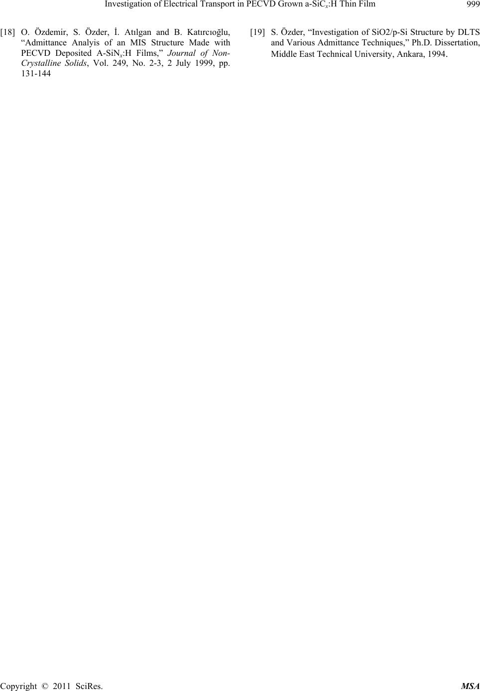 Investigation of Electrical Transport in PECVD Grown a-SiCx:H Thin Film Copyright © 2011 SciRes. MSA 999 [18] O. Özdemir, S. Özder, İ. Atılgan and B. Katırcıoğlu, “Admittance Analyis of an MIS Structure Made with PECVD Deposited A-SiNx:H Films,” Journal of Non- Crystalline Solids, Vol. 249, No. 2-3, 2 July 1999, pp. 131-144 [19] S. Özder, “Investigation of SiO2/p-Si Structure by DLTS and Various Admittance Techniques,” Ph.D. Dissertation, Middle East Technical University, Ankara, 1994. |