

Paper Menu >>
Journal Menu >>
 Materials Sciences and Applicatio n, 2011, 2, 765-770 doi:10.4236/msa.2011.27105 Published Online July 2011 (http://www.SciRP.org/journal/msa) Copyright © 2011 SciRes. MSA Structural and Dielectric Properties of Sintering Zinc Oxide Bulk Ceramic Mariem Chaari*, Adel Matoussi, Zouheir Fakhfakh 1Laboratory of Composite Ceramic and Polymer Materials, Scientific Faculty of Sfax, Tunisia, Africa. Email: *[email protected] Received April 2nd, 2011; revised April 22nd, 2011; accepted April 30th, 2011. ABSTRACT Undoped zinc oxide (ZnO) has been prepared at various growth temperatures by conventional sintering process. The morphology and crystalline properties of ZnO pellets were examined by scanning electron microscopy, atomic force microscopy and X-ray diffraction. It has revealed that the grain size and surface roughness tends to increase by in- creasing the sintering temperature. XRD analysis showed that all samples are polycrystalline with a hexagonal wurtzite structure. The alignment of ZnO grains along the (10.0) plane was enhanced as the temperature increased. Interestingly, the compressive stress was found to decrease drastically from –0.62 GPa at 700˚C to –0.2 MPa at 1000˚C. This im- provement in film structure seems to enhance considerably the dielectric properties for the samples sintering at high temperatures. Results show an increase of dielectric constant and a decrease of electrical resistivity when increasing the sintering temperature. Keywords: Zinc Oxide, Sintering Process, Micro Strain, Impedance Spectroscopy 1. Introduction During the last few decades, zinc oxide (ZnO) has at- tracted much interest in science and technology due to its versatile properties such as transparency in the visible range, direct band gap (3.37 eV), absence of toxicity, abundance in nature, etc. These characteristics find a wide range of applications in opto-electronic and electronic de- vices [1-7]. For example, it used in solar cells [1], trans- parent conducting films, chemical sensors [2,3], varistors [4,5], light-emitting diodes[6], laser diodes [7], etc. The preparation of high quality ZnO thin films has been the subject of continuous research. Many tech- niques are used for preparing zinc oxide such as: RF sputtering [8], chemical vapour deposition [9], sol-gel process [10], carbothermal reduction method [11] and pressurized melt growth [12,13], among others. The conventional sintering process has the advantages of be- ing cheap, easy-to-use, safe and able to be implemented in a standard laboratory. It is well known that the opto- electronic properties of ZnO are affected by the prepara- tion conditions such as working pressure, substrate tem- perature, types of substrates, thickness of the films and annealing temperature. The present paper is devoted to examine the influ- ence of sintering temperature on the structure, mor- phological and the dielectric properties of ZnO tablets. 2. Experimental Procedure Undoped ZnO pellets were prepared by the conventional sintering technique in an atmospheric heated furnace using zinc oxide powders (Aldrich-GmbH, purity ≈99%). The ZnO powders were first milled in an agate mortar and heated in air at annealing temperature of 300˚C for 2 hours to evaporate the water and remove the organic re- siduals. The obtained powders were then pressed into pellet disks (of about 1mm thickness and 8 mm diameter) and sintered at various temperatures (700˚C - 1000˚C) in ambient air for 3 hours. Finally, these pellets were rapidly quenched to room temperature in air in order to freeze the structure. The crystalline structure and surface morphol- ogy of the sintered specimens were characterized by X-ray diffraction (XRD), scanning electron microscopy (SEM) and atomic force microscopy (AFM). The spec- trometer dielectric was used to characterize the dielectric properties of the obtained samples. 3. Results and Discussions 3.1. Structural Properties The ZnO structure is examined by θ - 2θ X-ray diffrac- tion (XRD) measurements. Figure 1 shows the XRD  Structural and Dielectric Properties of Sintering Zinc Oxide Bulk Ceramic 766 patterns of ZnO prepared at growth temperature ranging from 700˚C to 1000˚C. All the samples exhibit a poly- crystalline hexagonal structure. The peaks are identified to (10.0), (00.2), (10.1), (10.2), (11.0) and (10.3) plane reflections for wurtzite phase of ZnO according to the standard JCPDS data file (No. 36-1451). One can see that the ZnO growth appears to be randomly oriented along the (10.1) plane instead of c-axis (00.2) direction. In order to evaluate the texture coefficient and the per- centages in volume of oriented crystallites in the <hk.l> direction, we have used the well-known formula reported in Ref. [14] and results are given in Table 1. It is found that the highest value of texture coefficient (TC) corresponds to (10.1) plane which contributes about 47 % of oriented ZnO grains. We notice a slight decrease of the contribution of (00.2) phase on detriment to the (10. 1) one as the sintering temperature is varied from 700˚C to 1000˚C. Figure 2 shows that the intensity of the (10.1) peak compared to the neighboring (10.0) and (00.2) increases by increasing the sintering temperature from 700˚C to 1000˚C. This result indicates that (10.1) is the preferred orientation of ZnO pellet growth. In addition, the full width at half maximum (FWHM) for ZnO (10.1) peak decreases from 0.24˚ to 0.12˚ when the temperature increases from 700˚C to 1000˚C respectively. The dependence of the growth temperature on the grain size, the angle position and FWHM for ZnO (00.2) diffraction peak are illustrated in Table 2. The average grain size of ZnO is calculated using the Scherer’s Equa- tion [15]: 0.9 DBcos where D is the grain size, λ is the wavelength of the X-ray radiation used, B is the full width at half maximum (FWHM) of the diffraction peak and θ is the Bragg dif- fraction angle of the XRD peak. Figure 1. XRD patterns of ZnO prepared at various Sinter- ing temperatures. 700 750 800 0,45 0,50 0,55 0,60 0,65 0,70 0,75 Sintering temperature (˚C) Figure 2. Evolution of intensity ratio of XRD peaks as a function of sintering temperature. The crystallite size increases from approximately 38 nm at 700˚C to 52 nm at 900˚C. As the temperature in- creases, we observe a neat decrease of the full width at half maximum of the (00.2) peak. Furthermore, the (00.2) peak position shifts to higher angles and reaches the val- ue 34.408˚ of free-strained ZnO film [16]. Here, it must be pointed that the crystal quality of ZnO can be improved at higher sintering temperature [17-19]. This behavior can be explained by the reduction of the density defects and atom vacancies caused by the in- crease of the diffusion of oxygen and zinc atoms at ele- vated temperature. According to Bachari [20], the lack of oxygen atoms may result in the growth of non-stoi- chiometric thin films and bad crystalline phases. It has been reported that the crystalline properties and alignment of the ZnO thin films depends strongly on the substrate temperature and the O2 concentration during growth. Vimalkumar et al. [21] showed that with in- crease in the spray pyrolysis rate orientation of ZnO grains changed from (10.1) to (00.2) plane. Matsuka and Ono [22] have observed that the increase of oxygen par- tial pressure from 0 to 0.12 Pa leads to change of crystal- line orientation from (10.1) to (00.2) plane. Prasada et al. [23] showed that ZnO grows randomly along the (10.1), (00.2) and (10.0) orientations. They found that the stress value decreases whereas the particle size increases as the growth temperature increased. In our case, the lattice strain εzz and residual stress σ in the grown ZnO samples are estimated using the follow- ing expressions [24]: 2 1333 1112 13 2CC CC = 2C z z and 0 0 cc =c zz 2 (°) 45 50 55 60 T s =1000°C T s =850°C T s =700°C 25 30 35 40 XRD Intensity (u.a) (11-20) (10-12) (10-11) (0002) (10-10) 850900950 1000 I10.1/(I10.0+I00.2+I10.1) Copyright © 2011 SciRes. MSA  Structural and Dielectric Properties of Sintering Zinc Oxide Bulk Ceramic Copyright © 2011 SciRes. MSA 767 Table 1. Texture coefficient and percentages of oriented crystallites in <hk.l> direction. Ts (˚C) Texture coefficient TC(10.0) TC(00.2) TC(10.1) ±0.0005 ±0.0003 ±0.0004 Percentage of oriented crystallites (%) χ(10.0) χ(00.2) χ(10.1) 700 0.648 1.299 2.355 12.96 ± 0.008 25.99 ± 0.011 46.11 ± 0.012 800 0.639 1.312 2.345 12.78 ± 0.011 26.24 ± 0.020 47.10 ± 0.009 900 0.655 1.249 2.369 13.09 ± 0.007 24.98 ± 0.006 47.38 ± 0.004 1000 0.645 1.268 2.406 12.91 ± 0.005 25.36 ± 0.004 48.13 ± 0.003 Table 2. Variations of grain size and FWHM for ZnO (00.2) reflection with temperature. Ts (˚C) FWHM of the (00.2) peak (˚) Diffraction angle 2θ(˚) Grain size D(nm) 700 0.236 34.323 38.221 ± 0.021 800 0.209 34.353 41.323 ± 0.018 850 0.183 34.386 47.194 ± 0.011 900 0.168 34.403 51.407 ± 0.017 1000 0.172 34.420 50.212 ± 0.013 where c0 and c are the lattice parameters of unstrained and the prepared ZnO samples respectively. C11 = 209.7 GPa, C12 = 121.1 GPa, C13 = 105.1 GPa and C33 = 210.9 GPa are the elastic stiffness constants of bulk ZnO [23]. 0 5 10 15 20 25 30 700800850900 1000 Sintering temperature (°C) zz x10 -4 (a.u) -65 -55 -45 -35 -25 -15 -5 (x10 7 Pa) Figure 3 shows the variation of lattice strain and re- sidual stress in ZnO as a function of the growth tempera- ture. The sample sintered at 700˚C has larger strain and stress values. One can see that the residual stress is com- pressive which decreases negatively from –0.62 GPa at 700˚C to –0.2 MPa at 1000˚C. This means that elevated temperature in the range 900˚C - 1000˚C are favoured to obtain better crystalline quality of ZnO prepared by con- ventional sintering process. According to Prasada [23], the measured stress in ZnO is attributed mainly to intrinsic origins introduced by the presence of impurities defects and lattice distortions in the crystal. The extrinsic stress induced by the lattice and the thermal mismatches will not be generated because the pellet is thicker (1 mm - 2 mm) and because of the non-use of growth substrate in our experiment. Figure 3. Variation of lattice strain and residual stress in ZnO tablet s. Table 3. EDX analysis of the Zinc oxide samples. Sintering temperature(˚C) O (at %) Zn (at %) 700 50.568 ± 0.008 48.144 ± 0.006 850 50.043 ± 0.005 48.244 ± 0.009 900 49.752 ± 0.011 48.76 ± 0.011 1000 49.412 ± 0.012 49.78 ± 0.013 Moreover, it is shown that the intrinsic stress appears frequently in nonstoichiometric films [23,25]. This seems to be consistent with energy dispersive X-ray (EDX) analysis presented in the Table 3. It is seen clearly that the sample composition became more stoichiometric with in- creasing the sintering temperature. For all the samples, the level of incorporation impurity is reduced to an amount lesser than 1.5% and the percentages of oxygen and the zinc are nearly equal. Consequently, it reveals that the growth at high temperature (>1000˚C) can strongly en- hance the physicochemical properties and thus improve the crystallinity of the ZnO films. pellets sintered at 850˚C, 900˚C and 1000˚C. For all samples, the surface is rough and presents grains of crys- tallites having very varied shapes and nanometric sizes. These crystallites are randomly distributed and irregu- larly disoriented. With increasing the sintering tempera- ture, the grain size is found to increase whereas its den- sity decreases resulting from conglomeration or coales- cence of smaller grains. Here, it is evident that the sintering temperature exer- cises strong effects on the surface morphology and the crystal quality of ZnO powders. 3.2. Morphological Properties Figure 4 shows the scanning electron micrographs of ZnO  Structural and Dielectric Properties of Sintering Zinc Oxide Bulk Ceramic 768 Figure 4. Plan view of SEM micrographs of ZnO pellets sintered at 850˚C (a); 900˚C (b); and 1000˚C (c). From AFM analyses, the rms roughness increases from 9 nm to 68 nm as the deposition temperature increases from 700˚C to 1000˚C. This agrees well with the results of XRD measurements. We surmise that at high tem- perature, the atoms have enough diffusion activation en- ergy to occupy the proper sites in the crystal lattice and grains with the lower surface energy become larger at high temperature [26]. These results show that the high temperature enhances the coalescence of grains and thus the lateral growth of ZnO along the <10.1> direction. 3.3. Dielectric Analysis Figure 5 presents the variation of the dielectric constant measured at room temperature for different frequency as a function of the sintering temperature. The dielectric constant was decreased as the measuring frequency in- creased. For the sample sintered at 1000˚C the ε value decreased from 900 at 1 Hz to 12.27 at 2 kHz and to 4 at 1 MHz. Also, it shows an increase tendency of all the dielectric constants with increasing the sintering tem- perature from 700˚C to 1000˚C. (a) These behaviours may be attributed to the enhance- ment of grain size, compactness and the structural quality of the material [25-27]. Figure 6 illustrates the evolution of electrical resistivity with increasing the sintering tem- perature. The resistivity was first decreased reaching a minimum value 4 × 10⁹ Ω·cm at 850˚C and then in- creased with increasing temperature. A similar behaviour has been observed by Gomes [28] and Olivera [29] in Ga- doped and F-doped ZnO thin films, respectively. (b) The measured values of resistivity are in range 109 - 1010 Ω·cm which indicates that our prepared ZnO bulk possess an insulating behaviour rather than n-type semi- 1 10 100 1000 650750850950 1050 Sintering temperature (°C) Dielectric constant (a.u) 1Hz 100Hz 10KHz 1MHz (c) Figure 5. Vari atio n of the di elec tric constant as a func tion of the sintering temperature. 1 5 9 13 17 650 750850 9501050 Sintering temperature (°C) Resistivity (x10 9 Ω.cm ) Figure 6. Evolution of electrical resistivity versus the sin- tering temperature. Copyright © 2011 SciRes. MSA  Structural and Dielectric Properties of Sintering Zinc Oxide Bulk Ceramic769 conductor character. However, the decrease of resistivity with elevation of growth temperature is due, on the one hand, to both the improvement in the pellet structure and the reduction of grain boundaries which enhance the free electron mobility [30]. On the other hand, the reduction in the resistivity can also be due to the non-stoichiometry of the film and the presence of residual impurities (K, Ca, S, and Fe) which can substitute the Zn atoms and/or be incorporated in oxygen vacancies [28,29,31]. For samples sintered at higher temperatures, the in- crease in resistivity can be associated to more appropriate stoichiometry, the increase of ZnO grain size and the scattering of free carriers at grain boundaries in poly- crystalline ZnO pellets [23-25]. Here, it is important to notice that high temperature can enhance the crystalline and the dielectric properties of ZnO pellets. As schown in Figure 7, the lowest value of dielectric loss at higher frequencies (tg δ = 6.6 × 10⁻²) is found for the ZnO sample sintered at 900˚C. Due to their good di- electric properties, low dielectric loss, and high electrical resistivity. ZnO can be used as a promising material for fabrication of dielectric varistors and transparent elec- trodes in solar cells. 4. Conclusions In this paper, we study the effect of growth temperature on the structural and dielectric properties of zinc oxide prepared by conventional sintering process. The mor- phology and the crystalline characteristics of ZnO films were examined by scanning electron microscopy, atomic force microscopy, and X-ray diffraction. It has revealed that the grain size and surface roughness tends to increase and that the crystalline quality of ZnO film is better en- hanced by increasing the sintering temperature. XRD analysis showed that all films are polycrystalline with a hexagonal wurtzite structure and randomly ori- ented (10.1) direction. The residual stress in ZnO sample 0,00 0,05 0,10 0,15 0,20 0,25 0,30 0,35 0,40 700 750800 850 900 95010001050 Sintering temperature (°C) Dielectric loss (u.a) f=1MHz f=10M Hz Figure 7. Variation of the dielectric loss versus the sintering temperature. is compressive which decreases significantly from –0.62 GPa at 700˚C to –0.2 MPa at 1000˚C. The temperature dependence of electrical resistivity and dielectric constant were studied at room temperature for different frequen- cies ranging from 10–1 Hz until 10 MHz. Results show an increase of dielectric constants with increasing the sin- tering temperature and a decrease with changing the measuring frequency. This effect is attributed to the in- crease of grain size, deviation from stoichiometry and the decrease in sample strain. Electrical resistivity was determined to be in the range 4 × 10⁹ - 2.4 × 10¹⁰ Ω·cm indicating a more dielectric be- haviour than a semi-conducting character. All the above results show that the sample sintered at 900˚C has the best dielectric properties and a good crystalline structure. REFERENCES [1] S. Gledhil, A. Grimm, A. Allsop, T. Koehler, C. Camus, L. Lux-Steiner and C.-H. Fisher, “A Spray Pyrolysis Route to the Undoped ZnO Layer of Cu(In,Ga)(S,Se)2 Solar Cells,” Thin Solid Films, Vol. 517, No. 7, 2009, pp. 2309-2311. doi:10.1016/j.tsf.2008.10.110 [2] S. Major and K. L. Chopra, “Indium-Doped Zinc Oxide Films as Transparent Electrodes for Solar Cells,” Solar Energy Materials, Vol. 17, No. 5, 1988, pp. 319-327. doi:10.1016/0165-1633(88)90014-7 [3] S. T. Shishiyanu, T. S. Shishiyanu and O. I. Lu- pan,“Sensing Characteristics of Tin-Doped ZnO Thin films as NO2 Gas Sensor,” Sensors and Actuators B: Chemical, Vol. 107, No. 1, 2005, pp. 379-386. doi:10.1016/j.snb.2004.10.030 [4] T. K. Gupta and J. Am, “Application of Zinc Oxide Varistors,” American Ceramatic Society, Vol. 73, No. 7, 1990, pp. 1817-1840. doi:10.1111/j.1151-2916.1990.tb05232.x [5] S. Anas, R. V. Mangalaraja, M. Poothayal, S. K. Shukla and S. Ananthakumar, “Direct Synthesis of Varistor- Grade Doped Nanocrystalline ZnO and Its Densification through a Step-Sintering Technique,” Acta Materialia, Vol. 55, No. 17, 2007, pp. 5792-5801. doi:10.1016/j.actamat.2007.06.047 0.40 0.35 [6] Y. I. Alivov, E. V. Kalinina, A. E. Cherenkov, D. C. Look, B. M. Ataev, A. K. Omaev, M. V. Chukichev and D. M. Bagnall, “Fabrication and Characterization of n-ZnO/ p-AlGaN Heterojunction Light-Emitting Diodes on 6H-SiC Substrates,” Applied Physics Letters, Vol. 83, No. 23, 2003, pp. 4719-4721. doi:10.1063/1.1632537 0.30 0.25 0.20 0.15 [7] H. S. Kim, F. Lugo, S. J. Pearton, D. P. Norton, Y. L. Wang and F. Ren, “Phosphorus Doped ZnO Light Emit- ting Diodes Fabricated via Pulsed Laser Deposition,” Ap- plied Physics Letters, Vol. 92, No. 11, 2008, pp. 112108- 112110. doi:10.1063/1.2900711 0.10 0.05 0.00 [8] X. H. Yu, J. Ma, F. Ji, Y. H. Wang, X. J. Zhang and H. L. Ma, “Influence of Annealing on the Properties of ZnO: Ga Films Prepared by Radio Frequency Magnetron Sputter- ing,” Thin Solid Films, Vol. 483, No. 1-2, 2005, pp. Copyright © 2011 SciRes. MSA 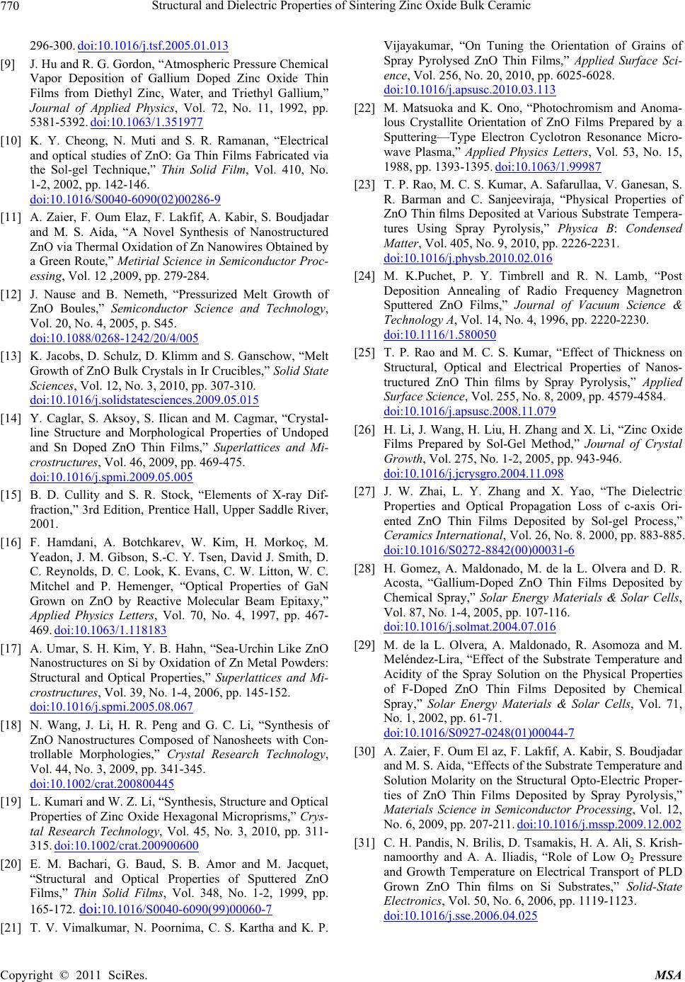 Structural and Dielectric Properties of Sintering Zinc Oxide Bulk Ceramic Copyright © 2011 SciRes. MSA 770 296-300. doi:10.1016/j.tsf.2005.01.013 [9] J. Hu and R. G. Gordon, “Atmospheric Pressure Chemical Vapor Deposition of Gallium Doped Zinc Oxide Thin Films from Diethyl Zinc, Water, and Triethyl Gallium,” Journal of Applied Physics, Vol. 72, No. 11, 1992, pp. 5381-5392. doi:10.1063/1.351977 [10] K. Y. Cheong, N. Muti and S. R. Ramanan, “Electrical and optical studies of ZnO: Ga Thin Films Fabricated via the Sol-gel Technique,” Thin Solid Film, Vol. 410, No. 1-2, 2002, pp. 142-146. doi:10.1016/S0040-6090(02)00286-9 [11] A. Zaier, F. Oum Elaz, F. Lakfif, A. Kabir, S. Boudjadar and M. S. Aida, “A Novel Synthesis of Nanostructured ZnO via Thermal Oxidation of Zn Nanowires Obtained by a Green Route,” Metirial Science in Semiconductor Proc- essing, Vol. 12 ,2009, pp. 279-284. [12] J. Nause and B. Nemeth, “Pressurized Melt Growth of ZnO Boules,” Semiconductor Science and Technology, Vol. 20, No. 4, 2005, p. S45. doi:10.1088/0268-1242/20/4/005 [13] K. Jacobs, D. Schulz, D. Klimm and S. Ganschow, “Melt Growth of ZnO Bulk Crystals in Ir Crucibles,” Solid State Sciences, Vol. 12, No. 3, 2010, pp. 307-310. doi:10.1016/j.solidstatesciences.2009.05.015 [14] Y. Caglar, S. Aksoy, S. Ilican and M. Cagmar, “Crystal- line Structure and Morphological Properties of Undoped and Sn Doped ZnO Thin Films,” Superlattices and Mi- crostructures, Vol. 46, 2009, pp. 469-475. doi:10.1016/j.spmi.2009.05.005 [15] B. D. Cullity and S. R. Stock, “Elements of X-ray Dif- fraction,” 3rd Edition, Prentice Hall, Upper Saddle River, 2001. [16] F. Hamdani, A. Botchkarev, W. Kim, H. Morkoç, M. Yeadon, J. M. Gibson, S.-C. Y. Tsen, David J. Smith, D. C. Reynolds, D. C. Look, K. Evans, C. W. Litton, W. C. Mitchel and P. Hemenger, “Optical Properties of GaN Grown on ZnO by Reactive Molecular Beam Epitaxy,” Applied Physics Letters, Vol. 70, No. 4, 1997, pp. 467- 469. doi:10.1063/1.118183 [17] A. Umar, S. H. Kim, Y. B. Hahn, “Sea-Urchin Like ZnO Nanostructures on Si by Oxidation of Zn Metal Powders: Structural and Optical Properties,” Superlattices and Mi- crostructures, Vol. 39, No. 1-4, 2006, pp. 145-152. doi:10.1016/j.spmi.2005.08.067 [18] N. Wang, J. Li, H. R. Peng and G. C. Li, “Synthesis of ZnO Nanostructures Composed of Nanosheets with Con- trollable Morphologies,” Crystal Research Technology, Vol. 44, No. 3, 2009, pp. 341-345. doi:10.1002/crat.200800445 [19] L. Kumari and W. Z. Li, “Synthesis, Structure and Optical Properties of Zinc Oxide Hexagonal Microprisms,” Crys- tal Research Technology, Vol. 45, No. 3, 2010, pp. 311- 315. doi:10.1002/crat.200900600 [20] E. M. Bachari, G. Baud, S. B. Amor and M. Jacquet, “Structural and Optical Properties of Sputtered ZnO Films,” Thin Solid Films, Vol. 348, No. 1-2, 1999, pp. 165-172. doi:10.1016/S0040-6090(99)00060-7 [21] T. V. Vimalkumar, N. Poornima, C. S. Kartha and K. P. Vijayakumar, “On Tuning the Orientation of Grains of Spray Pyrolysed ZnO Thin Films,” Applied Surface Sci- ence, Vol. 256, No. 20, 2010, pp. 6025-6028. doi:10.1016/j.apsusc.2010.03.113 [22] M. Matsuoka and K. Ono, “Photochromism and Anoma- lous Crystallite Orientation of ZnO Films Prepared by a Sputtering—Type Electron Cyclotron Resonance Micro- wave Plasma,” Applied Physics Letters, Vol. 53, No. 15, 1988, pp. 1393-1395. doi:10.1063/1.99987 [23] T. P. Rao, M. C. S. Kumar, A. Safarullaa, V. Ganesan, S. R. Barman and C. Sanjeeviraja, “Physical Properties of ZnO Thin films Deposited at Various Substrate Tempera- tures Using Spray Pyrolysis,” Physica B: Condensed Matter, Vol. 405, No. 9, 2010, pp. 2226-2231. doi:10.1016/j.physb.2010.02.016 [24] M. K.Puchet, P. Y. Timbrell and R. N. Lamb, “Post Deposition Annealing of Radio Frequency Magnetron Sputtered ZnO Films,” Journal of Vacuum Science & Technology A, Vol. 14, No. 4, 1996, pp. 2220-2230. doi:10.1116/1.580050 [25] T. P. Rao and M. C. S. Kumar, “Effect of Thickness on Structural, Optical and Electrical Properties of Nanos- tructured ZnO Thin films by Spray Pyrolysis,” Applied Surface Science, Vol. 255, No. 8, 2009, pp. 4579-4584. doi:10.1016/j.apsusc.2008.11.079 [26] H. Li, J. Wang, H. Liu, H. Zhang and X. Li, “Zinc Oxide Films Prepared by Sol-Gel Method,” Journal of Crystal Growth, Vol. 275, No. 1-2, 2005, pp. 943-946. doi:10.1016/j.jcrysgro.2004.11.098 [27] J. W. Zhai, L. Y. Zhang and X. Yao, “The Dielectric Properties and Optical Propagation Loss of c-axis Ori- ented ZnO Thin Films Deposited by Sol-gel Process,” Ceramics International, Vol. 26, No. 8. 2000, pp. 883-885. doi:10.1016/S0272-8842(00)00031-6 [28] H. Gomez, A. Maldonado, M. de la L. Olvera and D. R. Acosta, “Gallium-Doped ZnO Thin Films Deposited by Chemical Spray,” Solar Energy Materials & Solar Cells, Vol. 87, No. 1-4, 2005, pp. 107-116. doi:10.1016/j.solmat.2004.07.016 [29] M. de la L. Olvera, A. Maldonado, R. Asomoza and M. Meléndez-Lira, “Effect of the Substrate Temperature and Acidity of the Spray Solution on the Physical Properties of F-Doped ZnO Thin Films Deposited by Chemical Spray,” Solar Energy Materials & Solar Cells, Vol. 71, No. 1, 2002, pp. 61-71. doi:10.1016/S0927-0248(01)00044-7 [30] A. Zaier, F. Oum El az, F. Lakfif, A. Kabir, S. Boudjadar and M. S. Aida, “Effects of the Substrate Temperature and Solution Molarity on the Structural Opto-Electric Proper- ties of ZnO Thin Films Deposited by Spray Pyrolysis,” Materials Science in Semiconductor Processing, Vol. 12, No. 6, 2009, pp. 207-211. doi:10.1016/j.mssp.2009.12.002 [31] C. H. Pandis, N. Brilis, D. Tsamakis, H. A. Ali, S. Krish- namoorthy and A. A. Iliadis, “Role of Low O2 Pressure and Growth Temperature on Electrical Transport of PLD Grown ZnO Thin films on Si Substrates,” Solid-State Electronics, Vol. 50, No. 6, 2006, pp. 1119-1123. doi:10.1016/j.sse.2006.04.025 |