

Paper Menu >>
Journal Menu >>
 Materials Sciences and Applicatio n, 2011, 2, 739-748 doi:10.4236/msa.2011.27102 Published Online July 2011 (http://www.SciRP.org/journal/msa) Copyright © 2011 SciRes. MSA Structural and Electrical Characterization of Sintered Silicon Nitride Ceramic Imran Khan, M. Zulfequar* Department of Physics, Jamia Millia Islamia, New Delhi, India. Email: [email protected] Received December 28th, 2010; revised March 28th, 2011; accepted May 5th, 2011. ABSTRACT The electrical conduction phenomena, dielectric response and microstructure have been discussed in sintered silicon nitride ceramics at different temperature and frequencies. Microstructure and phase of the sintered samples was inves- tigated by Scanning Electron Microscope (SEM) and X-ray diffractometer (XRD). The electrical conductivity, dielectric constant and dielectric loss increases exponentially with temperature greater than 600 K. The dielectric constant and loss have been measured in the frequency range 100 Hz to 1 MHz. The a.c. conduction studies in the audio frequency range 500 Hz to 1 MHz indicates that the conduction may be due to the electronic hopping mechanism. Silicon Nitride ceramics became dense after sintering. The effect of grain size and role of phase on electrical and dielectric properties have been discussed. These types of samples can be used as a high temperature semi conducting materials for device packaging. Keywords: Silicon Nitride, D.C. and A.C. Conductivity, Dielectric and Structural Properties 1. Introduction Silicon nitride-based ceramics have many excellent properties, high strength and relatively high fracture toughness, good wear resistance, good oxidation resis- tance and good corrosion resistance. For some time, they have been under consideration as high-performance structural materials because of their superior thermal shock resistance relative to oxide ceramics [1]. Silicon Nitride has been densified with sintering additives be- cause of the highly covalent Si-N bonding. After sintering, these additives remain as the amorphous grain boundary phase, which severely deteriorates the high-temperature mechanical behavior of Silicon Nitride ceramics [2]. Di- electric films of silicon nitride ceramics play an integral role in nearly every semiconductor device and integrated circuit. Among this Silicon Nitride ceramic is used as a gate dielectric layer, diffusion barrier and optoelec- tronic-integrated circuits [3-5]. Low-density porous sili- con nitride [6-12] ceramic is an important material with properties including low dielectric constant ( = 2.5 to 8, tan δ ≤ 3 × 10⁻³), good mechanical, high resistance to rain erosion and sand erosion. Hence, low-density porous silicon nitride ceramic is also a candidate for application in radome materials [13]. Microstructural control of the interface and interlayer requires a complex interplay between initial composition and post- heating transformations. The controlled crystallization of refractory secondary phases from the remaining oxyni- tride liquid generally results in an improvement of the high-temperature resistance of sintered Si3N4 ceramics [14-16]. Nowadays most silicon nitride ceramics are pre- pared using α-Si3N4 powders. In silicon nitride ceramics, the microstructure is similar to whisker-reinforced ce- ramic composites, with large rod like β-Si3N4 grains as the reinforcing agents [17]. The effect of microstructure or grain size on dielectric properties are also already dis- cussed [18]. In earlier studies on the micro structural cha- racterization of silicon nitrides ceramics, it is noted that all of them are conducted at relatively low TEM/SEM magnifications and therefore are limited to the examina- tion of the general microstructure. J. D Walten, P. Popper and J. S. Throp [19,20] reveal the kinetics of densification, mechanical, electrical and thermal properties of Si3N4 has been studied. However no such systematic effort had been made on the electrical conductivity and dielectric proper- ties of silicon nitride ceramic. The electrical conductivity and dielectrical measure- ment are very important to check the insulating ability and dielectric losses particularly at high temperatures. The emphasis of the research, in particular, is on the characterization of the grain-boundary microstructure by 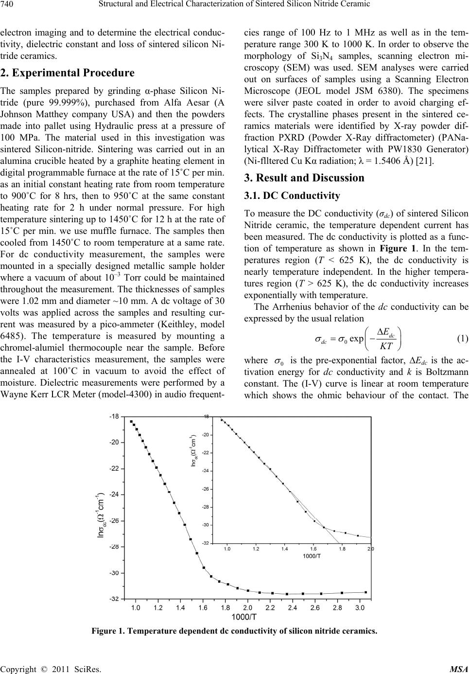 Structural and Electrical Characterization of Sintered Silicon Nitride Ceramic 740 electron imaging and to determine the electrical conduc- tivity, dielectric constant and loss of sintered silicon Ni- tride ceramics. 2. Experimental Procedure The samples prepared by grinding α-phase Silicon Ni- tride (pure 99.999%), purchased from Alfa Aesar (A Johnson Matthey company USA) and then the powders made into pallet using Hydraulic press at a pressure of 100 MPa. The material used in this investigation was sintered Silicon-nitride. Sintering was carried out in an alumina crucible heated by a graphite heating element in digital programmable furnace at the rate of 15˚C per min. as an initial constant heating rate from room temperature to 900˚C for 8 hrs, then to 950˚C at the same constant heating rate for 2 h under normal pressure. For high temperature sintering up to 1450˚C for 12 h at the rate of 15˚C per min. we use muffle furnace. The samples then cooled from 1450˚C to room temperature at a same rate. For dc conductivity measurement, the samples were mounted in a specially designed metallic sample holder where a vacuum of about 10–3 Torr could be maintained throughout the measurement. The thicknesses of samples were 1.02 mm and diameter ~10 mm. A dc voltage of 30 volts was applied across the samples and resulting cur- rent was measured by a pico-ammeter (Keithley, model 6485). The temperature is measured by mounting a chromel-alumiel thermocouple near the sample. Before the I-V characteristics measurement, the samples were annealed at 100˚C in vacuum to avoid the effect of moisture. Dielectric measurements were performed by a Wayne Kerr LCR Meter (model-4300) in audio frequent- cies range of 100 Hz to 1 MHz as well as in the tem- perature range 300 K to 1000 K. In order to observe the morphology of Si3N4 samples, scanning electron mi- croscopy (SEM) was used. SEM analyses were carried out on surfaces of samples using a Scanning Electron Microscope (JEOL model JSM 6380). The specimens were silver paste coated in order to avoid charging ef- fects. The crystalline phases present in the sintered ce- ramics materials were identified by X-ray powder dif- fraction PXRD (Powder X-Ray diffractometer) (PANa- lytical X-Ray Diffractometer with PW1830 Generator) (Ni-flltered Cu Kα radiation; λ = 1.5406 Å) [21]. 3. Result and Discussion 3.1. DC Conductivity To measure the DC conductivity (σdc) of sintered Silicon Nitride ceramic, the temperature dependent current has been measured. The dc conductivity is plotted as a func- tion of temperature as shown in Figure 1. In the tem- peratures region (T < 625 K), the dc conductivity is nearly temperature independent. In the higher tempera- tures region (T > 625 K), the dc conductivity increases exponentially with temperature. The Arrhenius behavior of the dc conductivity can be expressed by the usual relation 0exp dc dc E K T (1) where 0 is the pre-exponential factor, Edc is the ac- tivation energy for dc conductivity and k is Boltzmann constant. The (I-V) curve is linear at room temperature which shows the ohmic behaviour of the contact. The Figure 1. Temperature dependent dc c onduc tivity of silicon nitride ceramics. Copyright © 2011 SciRes. MSA 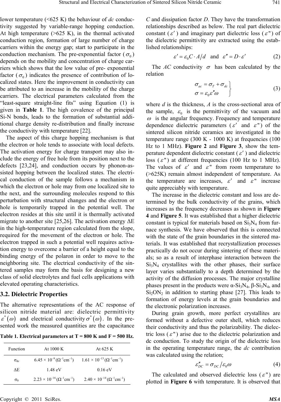 Structural and Electrical Characterization of Sintered Silicon Nitride Ceramic 741 lower temperature (<625 K) the behaviour of dc conduc- tivity suggested by variable-range hopping conduction. At high temperature (>625 K), in the thermal activated conduction region, formation of large number of charge carriers within the energy gap; start to participate in the conduction mechanism. The pre-exponential factor (0 ) depends on the mobility and concentration of charge car- riers which shows that the low value of pre- exponential factor (0 ) indicates the presence of contribution of lo- calized states. Here the improvement in conductivity can be attributed to an increase in the mobility of the charge carriers. The electrical parameters calculated from the “least-square straight-line fits” using Equation (1) is given in Table 1. The high covalence of the principal Si-N bonds, leads to the formation of substantial addi- tional charge density re-distribution and finally increase the conductivity with temperature [22]. The aspect of this charge hopping mechanism is that the electron or hole tends to associate with local defects. The activation energy for charge transport may also in- clude the energy of free hole from its position next to the defects [23,24], and conduction occurs by phonon-as- sisted hopping between the localized states. The electri- cal conduction of the sample follows a mechanism in which the electron or hole may from one localized site to the next, and the surrounding molecules respond to this perturbation with structural changes and the electron or hole is temporarily trapped in the potential well. The electron resides at this site until it is thermally activated migrate to another site [25,26]. The activation energy ΔE in the high-temperature region calculated from the slope, required for the movement of the electron or hole. The electron trapped in such a potential well requires activa- tion energy to overcome a barrier of a height equal to the binding energy of the polaron in order to move to the neighboring site. The electrical conductivity of the sin- tered samples may form the basis for designing a new class of solid electrolytes and fuel cells applications with elevated operating characteristics. 3.2. Dielectric Properties The alternative representations of the AC response of silicon nitride material are: dielectric permittivity * and electrical conductivity * . In the pre- sented work the measured quantities are the capacitance Table 1. Electrical parameters at T = 800 K and F = 500 Hz. Function At 1000 K At 625 K σdc 6.45 × 10⁻⁹ (Ω–1cm–1) 1.61 × 10⁻¹³ (Ω–1cm–1) ΔΕ 1.48 eV 0.16 eV σ0 2.23 × 10⁻¹⁶ (Ω–1cm–1) 2.40 × 10⁻¹⁴ (Ω–1cm–1) C and dissipation factor D. They have the transformation relationships described as below. The real part dielectric constant ( ) and imaginary part dielectric loss (" ) of the dielectric permittivity are extracted using the estab- lished relationships: 0CAd and D (2) The AC conductivity has been calculated by the relation 0 acT dc (3) where d is the thickness, A is the cross-sectional area of the sample, 0 is the permittivity of the vacuum and is the angular frequency. Frequency and temperature dependence dielectric parameters ( and " ) of the sintered silicon nitride ceramics are investigated in the temperature range (300 K - 1000 K) at frequencies (100 Hz to 1 MHz). Figure 2 and Figure 3, show the tem- perature dependent dielectric constant ( ) and dielectric loss (" ) at different frequencies (100 Hz to 1 MHz). The values of and " from room temperature to (>625K) remain almost independent of temperature. As the temperature are increases, and " increase quite appreciably with temperature. The increase in the dielectric constant and loss are de- termined by the bulk conductivity of the grains, which increases as the frequency decreases as shown in Figure 4 and Figure 5. It was established that a higher dielectric constant is typical for materials based on Si3N4 from fur- nace synthesis. We have observed that this is connected with the state of the grain boundaries in the sintered ma- terials. It was established that recrystallization processes practically do not occur during sintering of these materi- als; so as a result of interphase interaction between the Si3N4 crystallites with the other phases, their surface layer varies substantially to a depth determined by the activity of the diffusion processes. The major crystalline phases present in the products were α-Si3N4, β-Si3N4, and Si2ON2 in addition to starting phase [27]. This leads to formation of energy levels at the grain boundaries and the electronic polarization increases. During grain growth, more perfect crystallites are formed without a defective outer shell, which reduces their conductivity and thus the polarizability. The dielec- tric loss (" ) arise due to the dielectric polarization and dc conduction. To study the origin of the dielectric loss in the operating temperature range, the dc contribution was calculated using the relation; 0DC DC (4) The calculated and observed dielectric loss (" ) are plotted in Figure 6 with temperature. It is observed that Copyright © 2011 SciRes. MSA 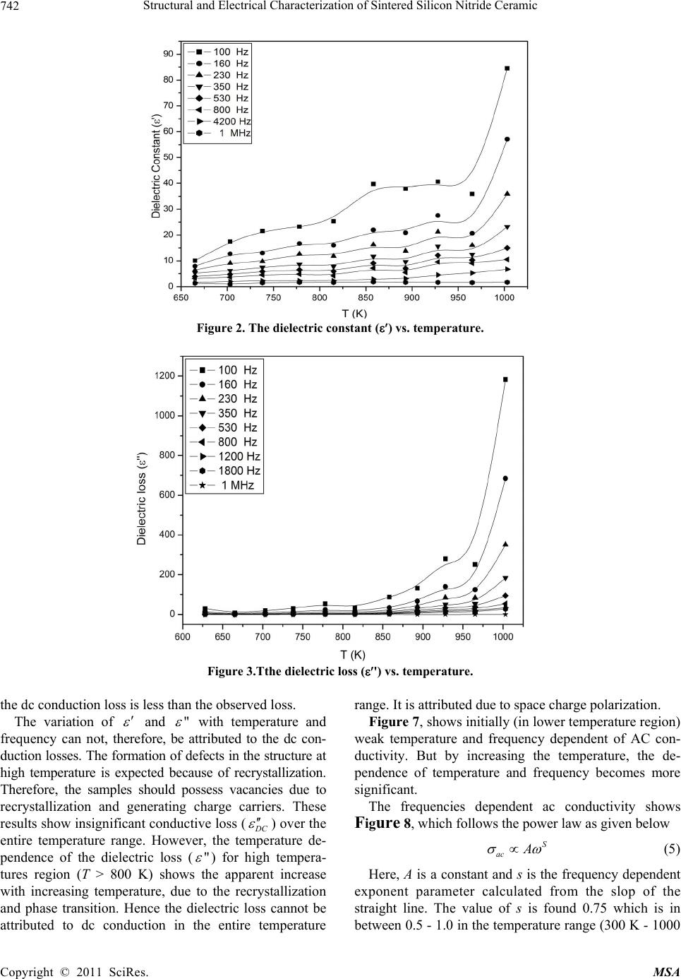 Structural and Electrical Characterization of Sintered Silicon Nitride Ceramic 742 Figure 2. The dielectric constant () vs. temperature. Figure 3.Tthe dielectric loss (') vs. temperature. the dc conduction loss is less than the observed loss. The variation of and " with temperature and frequency can not, therefore, be attributed to the dc con- duction losses. The formation of defects in the structure at high temperature is expected because of recrystallization. Therefore, the samples should possess vacancies due to recrystallization and generating charge carriers. These results show insignificant conductive loss ( D C ) over the entire temperature range. However, the temperature de- pendence of the dielectric loss (" ) for high tempera- tures region (T > 800 K) shows the apparent increase with increasing temperature, due to the recrystallization and phase transition. Hence the dielectric loss cannot be attributed to dc conduction in the entire temperature range. It is attributed due to space charge polarization. Figure 7, shows initially (in lower temperature region) weak temperature and frequency dependent of AC con- ductivity. But by increasing the temperature, the de- pendence of temperature and frequency becomes more significant. The frequencies dependent ac conductivity shows Figure 8, which follows the power law as given below S ac A (5) Here, A is a constant and s is the frequency dependent exponent parameter calculated from the slop of the straight line. The value of s is found 0.75 which is in between 0.5 - 1.0 in the temperature range (300 K - 1000 Copyright © 2011 SciRes. MSA 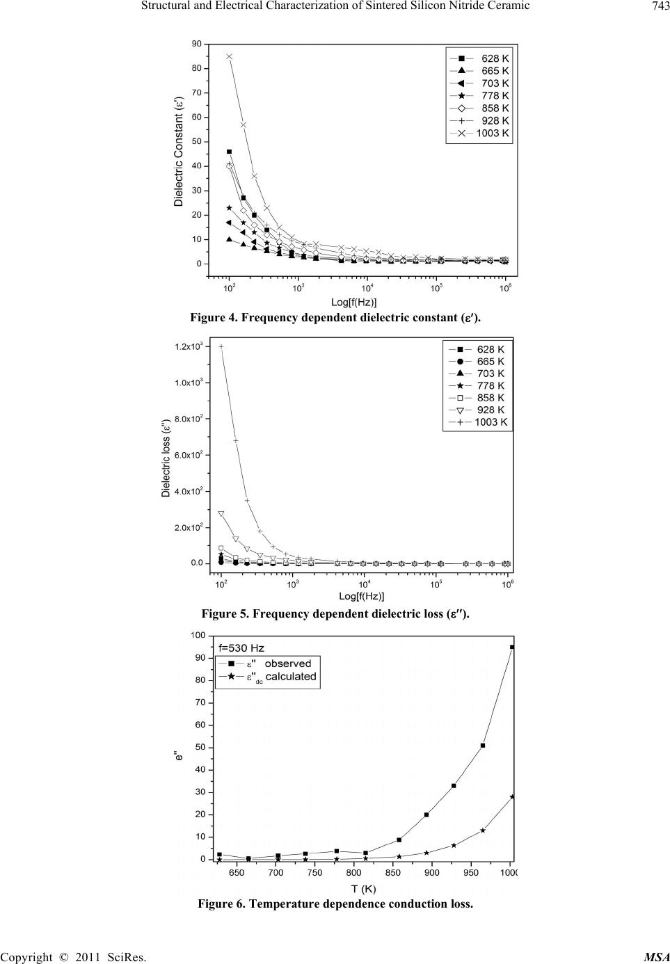 Structural and Electrical Characterization of Sintered Silicon Nitride Ceramic 743 Figure 4. Frequenc y de pendent dielectric constant (). Figure 5. Frequenc y de pendent dielectric loss (). Figure 6. Temperature depende nc e conduc tion loss. Copyright © 2011 SciRes. MSA 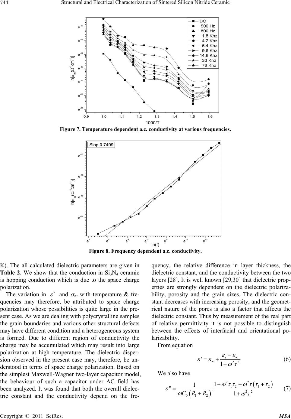 Structural and Electrical Characterization of Sintered Silicon Nitride Ceramic Copyright © 2011 SciRes. MSA 744 Figure 7. Temperature depende nt a.c. conductivity at various freque nc ie s. Figure 8. Frequenc y de pendent a.c. conductivity. K). The all calculated dielectric parameters are given in Table 2. We show that the conduction in Si3N4 ceramic is hopping conduction which is due to the space charge polarization. The variation in and ac with temperature & fre- quencies may therefore, be attributed to space charge polarization whose possibilities is quite large in the pre- sent case. As we are dealing with polycrystalline samples the grain boundaries and various other structural defects may have different condition and a heterogeneous system is formed. Due to different region of conductivity the charge may be accumulated which may result into large polarization at high temperature. The dielectric disper- sion observed in the present case may, therefore, be un- derstood in terms of space charge polarization. Based on the simplest Maxwell-Wagner two-layer capacitor model, the behaviour of such a capacitor under AC field has been analyzed. It was found that both the overall dielec- tric constant and the conductivity depend on the fre- quency, the relative difference in layer thickness, the dielectric constant, and the conductivity between the two layers [28]. It is well known [29,30] that dielectric prop- erties are strongly dependent on the dielectric polariza- bility, porosity and the grain sizes. The dielectric con- stant decreases with increasing porosity, and the geomet- rical nature of the pores is also a factor that affects the dielectric constant. Thus by measurement of the real part of relative permittivity it is not possible to distinguish between the effects of interfacial and orientational po- larizability. From equation 22 '1 s (6) We also have 22 121 2 22 01 2 1 1 ". 1 CR R (7) 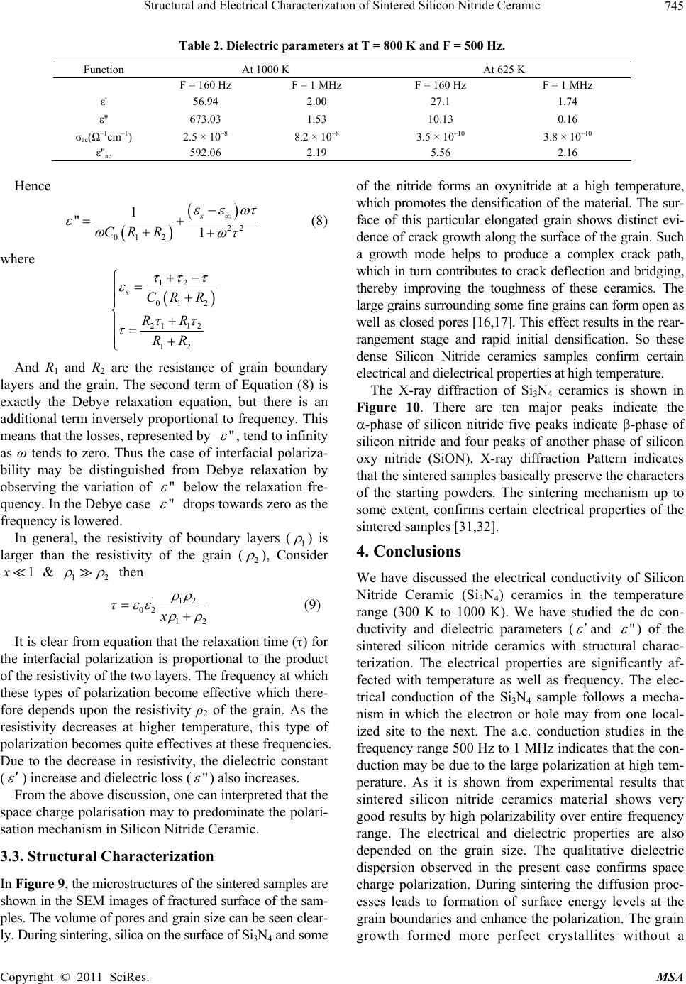 Structural and Electrical Characterization of Sintered Silicon Nitride Ceramic 745 Table 2. Dielectric parameters at T = 800 K and F = 500 Hz. Function At 1000 K At 625 K F = 160 Hz F = 1 MHz F = 160 Hz F = 1 MHz ε' 56.94 2.00 27.1 1.74 ε'' 673.03 1.53 10.13 0.16 σac(Ω–1cm–1) 2.5 × 10⁻⁸ 8.2 × 10⁻⁸ 3.5 × 10⁻¹⁰ 3.8 × 10⁻¹⁰ ε''ac 592.06 2.19 5.56 2.16 Hence 22 01 2 1 "1 s CR R (8) where 12 01 2 21 12 12 sCR R RR RR And R1 and R2 are the resistance of grain boundary layers and the grain. The second term of Equation (8) is exactly the Debye relaxation equation, but there is an additional term inversely proportional to frequency. This means that the losses, represented by " , tend to infinity as ω tends to zero. Thus the case of interfacial polariza- bility may be distinguished from Debye relaxation by observing the variation of " below the relaxation fre- quency. In the Debye case " drops towards zero as the frequency is lowered. In general, the resistivity of boundary layers (1 ) is larger than the resistivity of the grain (2 ), Consider & 1x12 then '12 02 12 x (9) It is clear from equation that the relaxation time (τ) for the interfacial polarization is proportional to the product of the resistivity of the two layers. The frequency at which these types of polarization become effective which there- fore depends upon the resistivity ρ2 of the grain. As the resistivity decreases at higher temperature, this type of polarization becomes quite effectives at these frequencies. Due to the decrease in resistivity, the dielectric constant ( ) increase and dielectric loss (" ) also increases. From the above discussion, one can interpreted that the space charge polarisation may to predominate the polari- sation mechanism in Silicon Nitride Ceramic. 3.3. Structural Characterization In Figu re 9, the microstructures of the sintered samples are shown in the SEM images of fractured surface of the sam- ples. The volume of pores and grain size can be seen clear- ly. During sintering, silica on the surface of Si3N4 and some of the nitride forms an oxynitride at a high temperature, which promotes the densification of the material. The sur- face of this particular elongated grain shows distinct evi- dence of crack growth along the surface of the grain. Such a growth mode helps to produce a complex crack path, which in turn contributes to crack deflection and bridging, thereby improving the toughness of these ceramics. The large grains surrounding some fine grains can form open as well as closed pores [16,17]. This effect results in the rear- rangement stage and rapid initial densification. So these dense Silicon Nitride ceramics samples confirm certain electrical and dielectrical properties at high temperature. The X-ray diffraction of Si3N4 ceramics is shown in Figure 10. There are ten major peaks indicate the -phase of silicon nitride five peaks indicate -phase of silicon nitride and four peaks of another phase of silicon oxy nitride (SiON). X-ray diffraction Pattern indicates that the sintered samples basically preserve the characters of the starting powders. The sintering mechanism up to some extent, confirms certain electrical properties of the sintered samples [31,32]. 4. Conclusions We have discussed the electrical conductivity of Silicon Nitride Ceramic (Si3N4) ceramics in the temperature range (300 K to 1000 K). We have studied the dc con- ductivity and dielectric parameters ( and " ) of the sintered silicon nitride ceramics with structural charac- terization. The electrical properties are significantly af- fected with temperature as well as frequency. The elec- trical conduction of the Si3N4 sample follows a mecha- nism in which the electron or hole may from one local- ized site to the next. The a.c. conduction studies in the frequency range 500 Hz to 1 MHz indicates that the con- duction may be due to the large polarization at high tem- perature. As it is shown from experimental results that sintered silicon nitride ceramics material shows very good results by high polarizability over entire frequency range. The electrical and dielectric properties are also depended on the grain size. The qualitative dielectric dispersion observed in the present case confirms space charge polarization. During sintering the diffusion proc- esses leads to formation of surface energy levels at the grain boundaries and enhance the polarization. The grain growth formed more perfect crystallites without a Copyright © 2011 SciRes. MSA 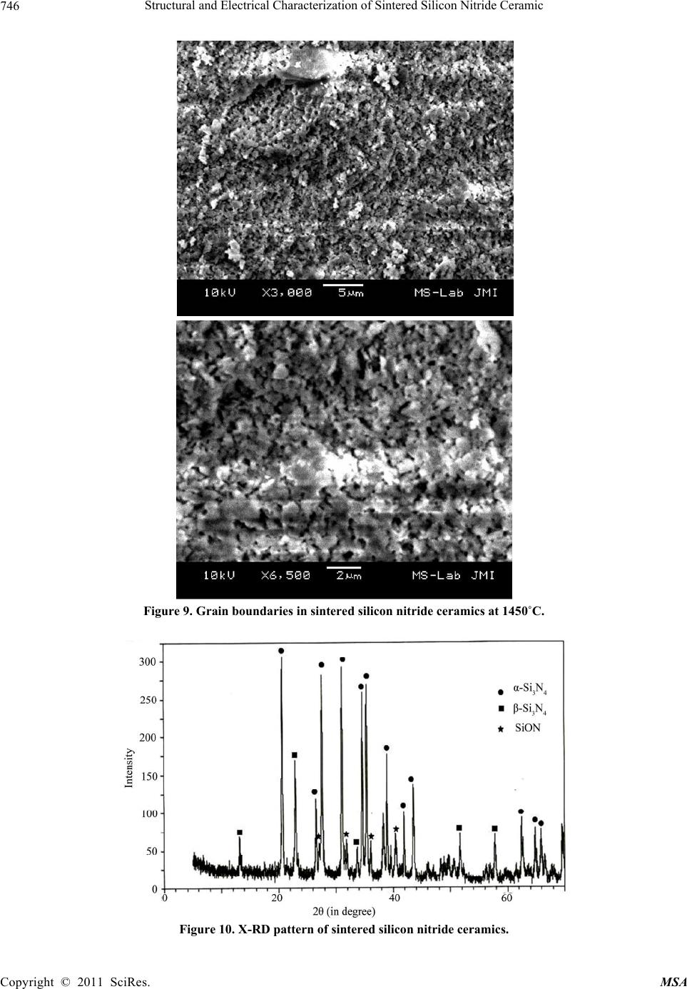 Structural and Electrical Characterization of Sintered Silicon Nitride Ceramic 746 Figure 9. Grain boundaries in sintered silicon nitride ceramics at 1450˚C. Figure 10. X-RD pattern of sintered silicon nitride ceramics. Copyright © 2011 SciRes. MSA  Structural and Electrical Characterization of Sintered Silicon Nitride Ceramic 747 defective outer shell. SEM images confirm the rear- rangement stage and rapid initial densification and X-ray diffraction pattern indicates that the sintered samples basically preserve the characters of the starting powders. These types of samples can be used as a high temperature semi conducting materials. REFERENCES [1] H.-J. Choi, J.-G. Lee and Y.-W. Kim, “High Temperature Strength and Oxidation Behavior of Hot-Pressed Silicon Nitride-Disilicate Ceramics,” Journal of Materials Scien- ce, Vol. 32, No. 7, 1997, pp. 1937-1942. [2] Y. S. Zheng, K. M. Knowles, J. M. Vieira, A. B. Lopes and F. J. Oliveira, “Microstructure, Toughness and Flex- ural Strength of Self-Reinforced Silicon Nitride Ceramics Doped with Yttrium Oxide and Ytterbium Oxide,” Jour- nal of Microscopy, Vol. 201, No. 2, 2001, pp. 238-249. doi:10.1046/j.1365-2818.2001.00839.x [3] I. Khan and M Zulfequar, “Effect of Tellurium on Elec- trical and Structural Properties of Sintered Silicon Nitride Ceramics,” Physica B, Vol. 404, No. 16, 2009, pp. 2395- 3400. doi:10.1016/j.physb.2009.04.050 [4] R. D. Gould, S. A. Awan, “DC Conductivity in RF Mag- netron Sputtered Gold–Silicon Nitride–Gold Sandwich Structures,” Thin Solid Film, Vol. 398-399, 2001, pp. 454-459. doi:10.1016/S0040-6090(01)01383-9 [5] M. C. Hugon, F. Delmotte, B. Agiusa and J. L. Courant, “Electrical Properties of Metal–Insulator–Semiconductor Structures with Silicon Nitride Dielectrics Deposited by Low Temperature Plasma Enhanced Chemical Vapor Deposition Distributed Electron Cyclotron Resonance,” Journal of Vacuum Science & Technology A, Vol. 15, No. 6, 1997, pp. 3143-3154. [6] J. H. She, J. F. Yang and D. J. Daniel, “Thermal Shock Behavior of Isotropic and Anisotropic Porous Silicon Ni- tride,” Journal of the American Ceramic Society, Vol. 86, No. 4, 2003, pp. 738-740. [7] S. K. Lee, J. D. Moretti, M. J. Readey and B. R. Lawn, “Thermal Shock Resistance of Silicon Nitrides Using an Indentation–Quench Test,” Journal of the American Ce- ramic Society, Vol. 85, No. 1, 2002, pp. 279-281. [8] S. Toshimori, “Shock Synthesis of Cubic Silicon Ni- tride,” Journal of the American Ceramic Society, Vol. 85, No. 1, 2002, pp. 113-116. [9] S. F. Dennis, J. O. Elizabeth and N. N. Quynhgiao, “Para- linear Oxidation of Silicon Nitride in a Water-Vapor/ Oxygen Environment,” Journal of the American Ceramic Society, Vol. 86, No. 8, 2003, pp. 1256-1261. [10] M. Backhaus-Ricoult, V. Guerin, A. M. Huntz and V. S. Urbanovich, “High-Temperature Oxidation Behavior of High-Purity α-, β-, and Mixed Silicon Nitride Ceramics,” Journal of the American Ceramic Society, Vol. 85, No. 2, 2002, pp. 385-392. [11] Y. Zhang, Y. B. Cheng S. Lathabai and K. Hirao, “Ero- sion Response of Highly Anisotropic Silicon Nitride,” Journal of the American Ceramic Society, Vol. 88, No. 1, 2005, pp. 114-120. [12] A. Zerr, M. Kempf, M. Schwarz, E. Kroke, M. Goken and R. Riedel, “Elastic Moduli and Hardness of Cubic Silicon Nitride,” Journal of the American Ceramic Society, Vol. 85, No. 1, 2002, pp. 86-90. [13] J. Barta, M. Manela and R. Fischer, “Si3N4 and Si2N2O for High Performance Radome,” Materials Science and Engineering, Vol. 71, 1984, pp. 265-272. [14] W. Braue, G. Wo¨tting and G. Ziegler, “Influence of Sin- tering Conditions on Mechanical Properties at Room and High Temperatures for Selected Y-Al-Si-O-N Materials,” Journal of Physics, Vol. 2, No. 47, 1986, pp. C1-341- C1-345. [15] G. D. Quinn and W. Braue, “Fracture Mechanism Maps for Advanced Structural Ceramics,” Journal of Materials Science, Vol. 25, No. 10, 1990, pp. 4377-4392. doi:10.1007/BF00581096 [16] M. H. Lewis, G. Leng-Ward and C. Jasper, “Sintering Additive Chemistry in Controlling Microstructure and Properties of Nitride Ceramics,” In: G. L. Messing, E. R. Fuller Jr. and H. Hausner, Eds., Ceramic Transactions, Vol. 1, Ceramic Powder Science II, Part B, American Ceramic Society, Westerville, OH, 1988, pp. 1019-1033. [17] A. Vuckovic, S. Boskovic and L. Zivkovic, “Synthesis of ‘in-Situ’ Reinforced Silicon Nitride Composites,” Journal of the Serbian Chemical Society, Vol. 69, No. 1, 2004, pp. 59-67. doi:10.2298/JSC0401059V [18] M. K. Park, H. N. Kim, K. S. Lee, S. S. Baek, E. S. Kang, Y. K. Baek and D. K. Kim, “Effect of Microstructure on Dielectric Properties of Si3N4 at Microwave Frequency,” Key Engineering Materials, Vol. 287, 2005, pp. 247-252. doi:10.4028/www.scientific.net/KEM.287.247 [19] J. D. Walton, Journal of the American Ceramic Society, Bull. 53, 1974, p. 255. [20] J. S. Throp and R. I. Sharif, “Dielectric Properties of Some Hot-Pressed Nitrogen Ceramics,” Journal of Mate- rials Science, Vol. 12, No. 11, 1977, pp. 2274-2280. doi:10.1007/BF00552249 [21] C. P. Gazzara, D. R. Messier, Journal of the American Ceramic Society, Vol. 78, 1977, p. 1076. [22] I. V. Kityk and P. Mandracci, “Nonlinear Optical Effects in Amorphous-Like SiCON Films,” Physics, Vol. 340, No. 5-6, June 2005, pp. 466-473. [23] D. F. Shriver, P. W. Atkins and C. H. Langford, “Inor- ganic Chemistry,” Freeman, New York, 1994. [24] K. F. Purcell and J. C. Kotz, “Inorganic Chemistry,” Saunders, Philadelphia, 1977. [25] M. M. El-Nahass, H. M. Zeyada, M. M. El-Samanoudy, E. M. El-Menyawy, Journal of Physics: Condensed Matter, Vol. 18, No. 22, 2006, p. 5163. doi:10.1088/0953-8984/18/22/016 [26] F. Yakuphanoglu, Y. Aydogdu, U. Schatzschneider and E. Rentschler, “DC and AC Conductivity and Dielectric Properties of the Metal-Radical Compound: Aqua[bis(2- dimethylaminomethyl-4-NIT-phenolato)]Copper(II),” So- lid State Communications, Vol. 128, No. 2-3, 2003, pp. 63-67. [27] M. Kara and A. Kerber, “Manufacture and Properties of Copyright © 2011 SciRes. MSA  Structural and Electrical Characterization of Sintered Silicon Nitride Ceramic Copyright © 2011 SciRes. MSA 748 Nitride Bonded Silicon Carbide Materials,” Fachberichte, Vol. 72, No. 6, 1995, pp. 325-328. [28] D. Liufu, X. S. Wang, D. M. Tu, and K. C. Kao, Journal of Applied Physics, “High-Field Induced Electrical Aging in Polypropylene Films,” Vol. 83, No. 4, 1998, p. 2209. doi:10.1063/1.366958 [29] H.-J. Choia, D.-H. Hanb, D.-S. Park, H.-D. Kimc, B.-D. Hanc, D.-S. Lima and I.-S. Kim, “Erosion Characteristics of Silicon Nitride Ceramics,” Ceramics International, Vol. Vol. 29, No. 6, 2003, pp. 713-719. [30] J.-F. Yang, T. Ohji, S. Kanzaki, A. Díaz and S. Hamp- shire, “Microstructure and Mechanical Properties of Sili- con Nitride Ceramics with Controlled Porosity,” Journal of the American Ceramic Society, Vol. 85, No. 6, 2002, pp. 1512-1516. [31] J. Xu, D. M. Zhu, F. Luo, W. C. Zhou and P. Li, “Dielec- tric Properties of Porous Reaction-Boned Si3N4 Ceramics with Controlled Porosity and Pore Size,” Journal of Ma- terials Science Technology, Vol. 24. No. 2, 2008, p. 207. [32] J. A. Schneider, S. H. Risbud, and A. K. Mukherjee, “Rapid Consolidation Processing of Silicon Nitride Pow- ders,” Journal of Materials Research, Vol. 11, No. 2, February 1996, pp. 358-362. doi:10.1557/JMR.1996.0043 |