

Paper Menu >>
Journal Menu >>
 Circuits and Systems, 2011, 2, 201-209 doi:10.4236/cs.2011.23029 Published Online July 2011 (http://www.SciRP.org/journal/cs) Copyright © 2011 SciRes. CS Chip Design of a Low-Voltage Wideband Continuous-Time Sigma-Delta Modulator with DWA Technology for WiMAX Applications Jhin-Fang Huang, Yan-Cheng Lai, Wen-Cheng Lai, Ron-Yi Liu Department of Electroni c En g i neerin g , National Taiwan University of Science and Technology, Chinese Taipei E-mail: [email protected] Received April 18, 2011; revised May 13, 2011; accepted May 20, 2011 Abstract This paper presents the design and experimental results of a continuous-time (CT) sigma-delta (ΣΔ) modula- tor with data-weighted average (DWA) technology for WiMAX applications. The proposed modulator com- prises a third-order active RC loop filter, internal quantizer operating at 160 MHz and three DAC circuits. A multi-bit quantizer is used to increase resolution and multi-bit non-return-to-zero (NRZ) DACs are adopted to reduce clock jitter sensitivity. The NRZ DAC circuits with quantizer excess loop delay compensation are set to be half the sampling period of the quantizer for increasing modulator stability. A dynamic element matching (DEM) technique is applied to multi-bit ΣΔ modulators to improve the nonlinearity of the internal DAC. This approach translates the harmonic distortion components of a nonideal DAC in the feedback loop of a ΣΔ modulator to high-frequency components. Capacitor tuning is utilized to overcome loop coefficient shifts due to process variations. The DWA technique is used for reducing DAC noise due to component mismatches. The prototype is implemented in TSMC 0.18 um CMOS process. Experimental results show that the ΣΔ modulator achieves 54-dB dynamic range, 51-dB SNR, and 48-dB SNDR over a 10-MHz signal bandwidth with an oversampling ratio (OSR) of 8, while dissipating 19.8 mW from a 1.2-V supply. Includ- ing pads, the chip area is 1.156 mm2. Keywords: ADC, Analog-to-Digital Conversion, Sigma-Delta Modulator, ΣΔ, DWA 1. Introduction Sigma-delta modulation techniques have been extended in moderate and high accuracy analog/mixed-signal IC applications, such as analog-to-digital data converters (ADCs), digital-to-analog data converters (DACs), fre- quency synthesizers, and power amplifiers [1]. Moreover, ΣΔ modulators are widely used in receivers because of their ability to provide high-resolution with relatively low precision components and low power consumption [2,3]. Oversampling ΣΔ ADCs trade digital signal proc- essing complexity for relaxed requirements on the analog components compared to Nyquist-rate ADCs [4]. Due to the over-sampling characteristics, ΣΔ modulators are limited on the application of voice band or lower fre- quency signals. As the ICs process is improved, recently it makes many researches transfer to wider bandwidth applications gradually, such as GSM, WCDMA, Blue- tooth, WiFi, and WiMAX [5]. With the progress of wireless communication, ADCs need higher OSR in or- der to achieve higher speed and resolution in the system. When OSR is programmable, increasing OSR leads to higher power consumption due to the increased speed requirement for the integrators and comparators in ΣΔ modulators. Due to the requirements of low supply volt- age and low power dissipation in the mobile communica- tions, the low order ΣΔ modulators of lower SNR are not suitable for wide bandwidth applications. Therefore, the high order multi-bit ΣΔ modulator circuit is design to increase the SNR. While most of current commercial ΣΔ ADCs for wire- less applications were implemented by using switched capacitor (SC) techniques which are also known as dis- crete-time (DT) ΣΔ ADCs [6-8], mainly due to mature design methodologies and robustness, more and more continuous-time (CT) ΣΔ ADCs were reported and showed impressive performance. Compared with DT counterparts, the CT ΣΔ ADCs have two main advan- 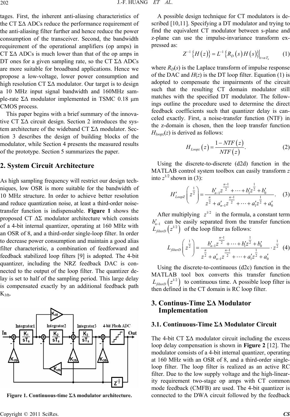 202 J.-F. HUANG ET AL. tages. First, the inherent anti-aliasing characteristics of the CT ΣΔ ADCs reduce the performance requirement of the anti-aliasing filter further and hence reduce the power consumption of the transceiver. Second, the bandwidth requirement of the operational amplifiers (op amps) in CT ΣΔ ADCs is much lower than that of the op amps in DT ones for a given sampling rate, so the CT ΣΔ ADCs are more suitable for broadband applications. Hence we propose a low-voltage, lower power consumption and high resolution CT ΣΔ modulator. Our target is to design a 10 MHz input signal bandwidth and 160MHz sam- ple-rate ΣΔ modulator implemented in TSMC 0.18 μm CMOS process. This paper begins with a brief summary of the innova- tive CT ΣΔ circuit design. Section 2 introduces the sys- tem architecture of the wideband CT ΣΔ modulator. Sec- tion 3 describes the design of building blocks of the modulator, while Section 4 presents the measured results of the prototype. Section 5 summarizes the paper. 2. System Circuit Architecture As high sampling frequency will restrict our design tech- niques, low OSR is more suitable for the bandwidth of 10 MHz structure. In order to achieve better resolution and reduce quantization noise, at least a third-order noise- transfer function is indispensable. Figure 1 shows the proposed CT ΔΣ modulator architecture which consists of a 4-bit internal quantizer, operating at 160 MHz with an OSR of 8, and a third-order single-loop filter. In order to decrease power consumption and maintain a good alias filter characteristic, a combination of feedforward and feedback stabilized loop filters [9] is adopted. The 4-bit quantizer, including the NRZ feedback DAC is con- nected to the output of the loop filter. The quantizer de- lay is set to half of the sampling period. This large delay is compensated exactly by an additional feedback path K3fb. Figure 1. Continuous-time ΣΔ modulator architecture. A possible design technique for CT modulators is de- scribed [10,11]. Specifying a DT modulator and trying to find the equivalent CT modulator between s-plane and z-plane can use the impulse-invariance transform ex- pressed as: 11 s DtnT ZHz LRsHs (1) where RD(s) is the Laplace transform of impulse response of the DAC and H(z) is the DT loop filter. Equation (1) is adopted to compensate the impairments of the circuit such that the resulting CT domain modulator still matches with the specified DT modulator. The follow- ings outline the procedure used to determine the direct feedback coefficients such that quantizer delay is can- celed exactly. First, a noise-transfer function (NTF) in the z-domain is chosen, then the loop transfer function Hloopz(z) is derived as follows: 1. Loopz NTF z HzNTF z (2) Using the discrete-to-discrete (d2d) function in the MATLAB control system toolbox can easily transform z into z1/2 shown in (3): 11 122 11 2 11 22 2 11 . n n LoopZ nn n bzbz b Hz zaz aza 0 0 (3) After multiplying in the formula, a constant term 1/2 z 1n b can be easily separated from the transfer function 1/ 2 rD z filte L of the loop filter as follows: 11 11 22 110 22 11 22 2 11 n n filterD nn n bzbz b Lz zaz aza 0 z (4) Using the discrete-to-continuous (d2c) function in the MATLAB tool box converts this transfer function 1/ 2 filterD Lz to continuous time. A possible loop filter is then defined in the CT domain is RC loop filter. 3. Continus-Time ΣΔ Modulator Implementation 3.1. Continuous-Time ΣΔ Modulator Circuit The 4-bit CT ΣΔ modulator circuit including the excess loop delay compensation is shown in Figure 2 [12]. The modulator consists of a 4-bit internal quantizer, operating at 160 MHz with an OSR of 8, and a third-order single- loop filter. The loop filter is realized as an active RC filter. Due to the low supply voltage and the high-linear- ity requirement two-stage op amps with CT common mode feedback (CMFB) are used. The 4-bit quantizer is connected to the DWA circuit followed by the feedback Copyright © 2011 SciRes. CS 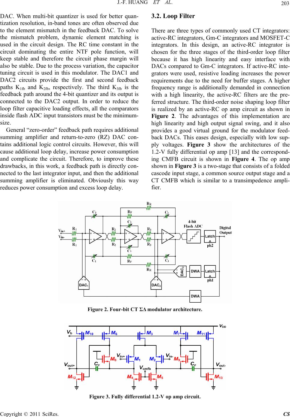 J.-F. HUANG ET AL. Copyright © 2011 SciRes. CS 203 3.2. Loop Filter DAC. When multi-bit quantizer is used for better quan- tization resolution, in-band tones are often observed due to the element mismatch in the feedback DAC. To solve the mismatch problem, dynamic element matching is used in the circuit design. The RC time constant in the circuit dominating the entire NTF pole function, will keep stable and therefore the circuit phase margin will also be stable. Due to the process variation, the capacitor tuning circuit is used in this modulator. The DAC1 and DAC2 circuits provide the first and second feedback paths K1fb and K2fb, respectively. The third K3fb is the feedback path around the 4-bit quantizer and its output is connected to the DAC2 output. In order to reduce the loop filter capacitive loading effects, all the comparators inside flash ADC input transistors must be the minimum- size. There are three types of commonly used CT integrators: active-RC integrators, Gm-C integrators and MOSFET-C integrators. In this design, an active-RC integrator is chosen for the three stages of the third-order loop filter because it has high linearity and easy interface with DACs compared to Gm-C integrators. If active-RC inte- grators were used, resistive loading increases the power requirements due to the need for buffer stages. A higher frequency range is additionally demanded in connection with a high linearity, the active-RC filters are the pre- ferred structure. The third-order noise shaping loop filter is realized by an active-RC op amp circuit as shown in Figure 2. The advantages of this implementation are high linearity and high output signal swing, and it also provides a good virtual ground for the modulator feed- back DACs. This eases design, especially with low sup- ply voltages. Figure 3 show the architectures of the 1.2-V fully differential op amp [13] and the correspond- ing CMFB circuit is shown in Figure 4. The op amp shown in Figure 3 is a two-stage that consists of a folded cascode input stage, a common source output stage and a CT CMFB which is similar to a transimpedence ampli- fier. General “zero-order” feedback path requires additional summing amplifier and return-to-zero (RZ) DAC con- tains additional logic control circuits. However, this will cause additional loop delay, increase power consumption and complicate the circuit. Therefore, to improve these drawbacks, in this work, a feedback path is directly con- nected to the last integrator input, and then the additional summing amplifier is eliminated. Obviously this way reduces power consumption and excess loop delay. Figure 2. Four-bit CT ΣΔ modulator architecture. Figure 3. Fully differential 1.2-V op amp circuit. 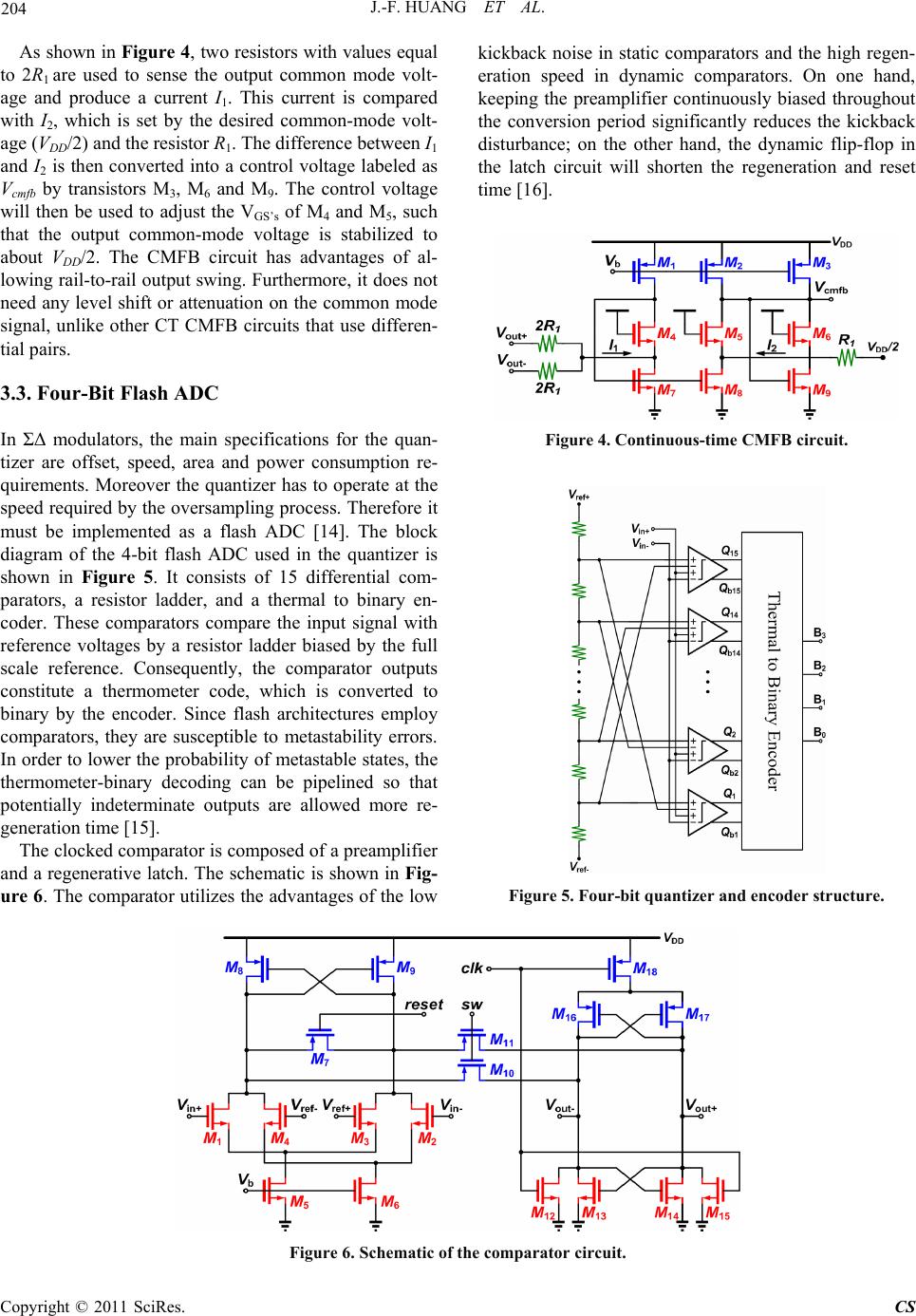 J.-F. HUANG ET AL. Copyright © 2011 SciRes. CS 204 As shown in Figure 4, two resistors with values equal to 2R1 are used to sense the output common mode volt- age and produce a current I1. This current is compared with I2, which is set by the desired common-mode volt- age (VDD/2) and the resistor R1. The difference between I1 and I2 is then converted into a control voltage labeled as Vcmfb by transistors M3, M6 and M9. The control voltage will then be used to adjust the VGS’s of M4 and M5, such that the output common-mode voltage is stabilized to about VDD/2. The CMFB circuit has advantages of al- lowing rail-to-rail output swing. Furthermore, it does not need any level shift or attenuation on the common mode signal, unlike other CT CMFB circuits that use differen- tial pairs. 3.3. Four-Bit Flash ADC In ΣΔ modulators, the main specifications for the quan- tizer are offset, speed, area and power consumption re- quirements. Moreover the quantizer has to operate at the speed required by the oversampling process. Therefore it must be implemented as a flash ADC [14]. The block diagram of the 4-bit flash ADC used in the quantizer is shown in Figure 5. It consists of 15 differential com- parators, a resistor ladder, and a thermal to binary en- coder. These comparators compare the input signal with reference voltages by a resistor ladder biased by the full scale reference. Consequently, the comparator outputs constitute a thermometer code, which is converted to binary by the encoder. Since flash architectures employ comparators, they are susceptible to metastability errors. In order to lower the probability of metastable states, the thermometer-binary decoding can be pipelined so that potentially indeterminate outputs are allowed more re- generation time [15]. The clocked comparator is composed of a preamplifier and a regenerative latch. The schematic is shown in Fig- ure 6. The comparator utilizes the advantages of the low kickback noise in static comparators and the high regen- eration speed in dynamic comparators. On one hand, keeping the preamplifier continuously biased throughout the conversion period significantly reduces the kickback disturbance; on the other hand, the dynamic flip-flop in the latch circuit will shorten the regeneration and reset time [16]. Figure 4. Continuous-time CMFB circuit. Figure 5. Four-bit quantizer and encoder structure. Figure 6. Schematic of the comparator circuit. 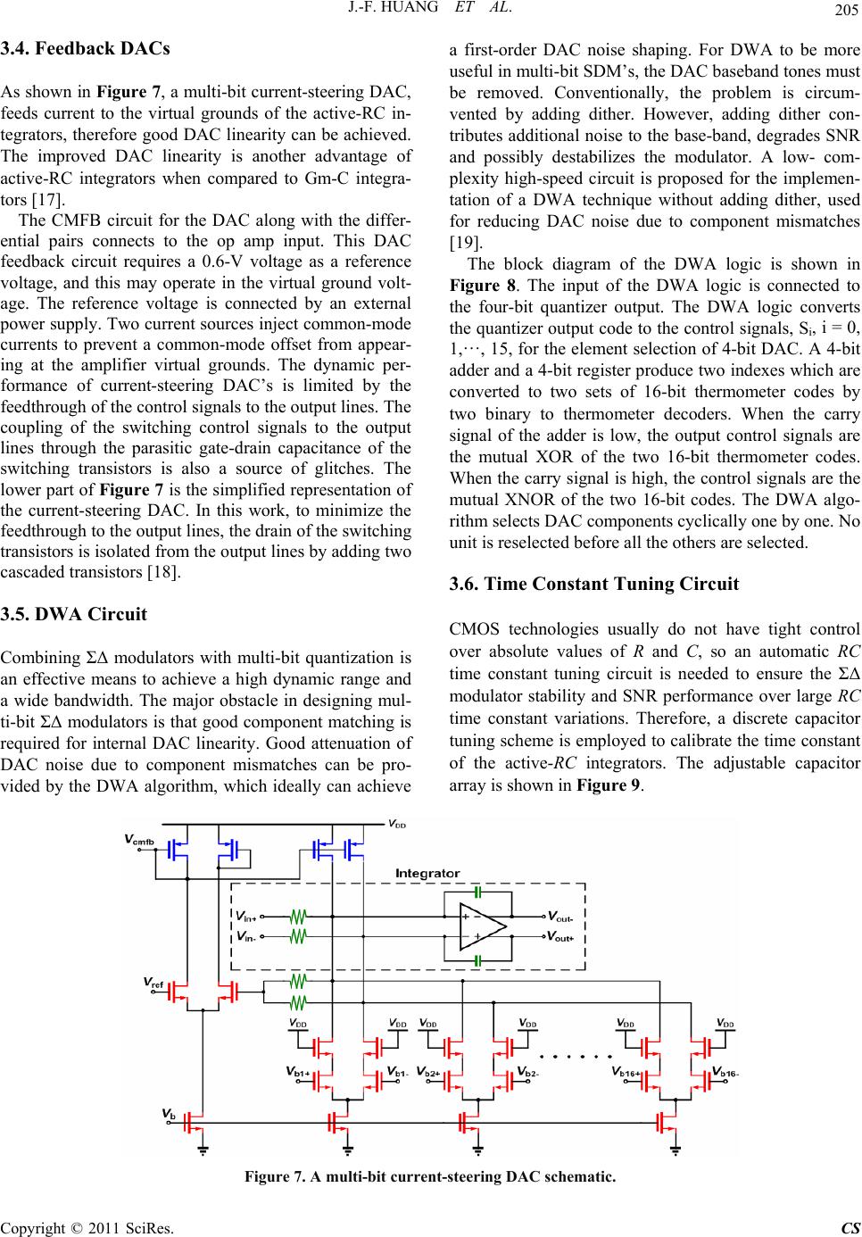 J.-F. HUANG ET AL. Copyright © 2011 SciRes. CS 205 3.4. Feedback DACs As shown in Figure 7, a multi-bit current-steering DAC, feeds current to the virtual grounds of the active-RC in- tegrators, therefore good DAC linearity can be achieved. The improved DAC linearity is another advantage of active-RC integrators when compared to Gm-C integra- tors [17]. The CMFB circuit for the DAC along with the differ- ential pairs connects to the op amp input. This DAC feedback circuit requires a 0.6-V voltage as a reference voltage, and this may operate in the virtual ground volt- age. The reference voltage is connected by an external power supply. Two current sources inject common-mode currents to prevent a common-mode offset from appear- ing at the amplifier virtual grounds. The dynamic per- formance of current-steering DAC’s is limited by the feedthrough of the control signals to the output lines. The coupling of the switching control signals to the output lines through the parasitic gate-drain capacitance of the switching transistors is also a source of glitches. The lower part of Figure 7 is the simplified representation of the current-steering DAC. In this work, to minimize the feedthrough to the output lines, the drain of the switching transistors is isolated from the output lines by adding two cascaded transistors [18]. 3.5. DWA Circuit Combining ΣΔ modulators with multi-bit quantization is an effective means to achieve a high dynamic range and a wide bandwidth. The major obstacle in designing mul- ti-bit ΣΔ modulators is that good component matching is required for internal DAC linearity. Good attenuation of DAC noise due to component mismatches can be pro- vided by the DWA algorithm, which ideally can achieve a first-order DAC noise shaping. For DWA to be more useful in multi-bit SDM’s, the DAC baseband tones must be removed. Conventionally, the problem is circum- vented by adding dither. However, adding dither con- tributes additional noise to the base-band, degrades SNR and possibly destabilizes the modulator. A low- com- plexity high-speed circuit is proposed for the implemen- tation of a DWA technique without adding dither, used for reducing DAC noise due to component mismatches [19]. The block diagram of the DWA logic is shown in Figure 8. The input of the DWA logic is connected to the four-bit quantizer output. The DWA logic converts the quantizer output code to the control signals, Si, i = 0, 1,…, 15, for the element selection of 4-bit DAC. A 4-bit adder and a 4-bit register produce two indexes which are converted to two sets of 16-bit thermometer codes by two binary to thermometer decoders. When the carry signal of the adder is low, the output control signals are the mutual XOR of the two 16-bit thermometer codes. When the carry signal is high, the control signals are the mutual XNOR of the two 16-bit codes. The DWA algo- rithm selects DAC components cyclically one by one. No unit is reselected before all the others are selected. 3.6. Time Constant Tuning Circuit CMOS technologies usually do not have tight control over absolute values of R and C, so an automatic RC time constant tuning circuit is needed to ensure the ΣΔ modulator stability and SNR performance over large RC time constant variations. Therefore, a discrete capacitor tuning scheme is employed to calibrate the time constant of the active-RC integrators. The adjustable capacitor array is shown in Figure 9. Figure 7. A multi-bit current-steering DAC schematic. 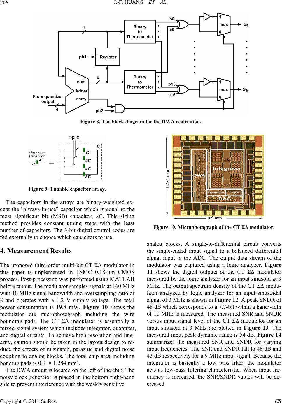 206 J.-F. HUANG ET AL. Figure 8. The block diagram for the DWA realization. Figure 9. Tunable capacitor array. The capacitors in the arrays are binary-weighted ex- cept the “always-in-use” capacitor which is equal to the most significant bit (MSB) capacitor, 8C. This sizing method provides constant tuning steps with the least number of capacitors. The 3-bit digital control codes are fed externally to choose which capacitors to use. 4. Measurement Results The proposed third-order multi-bit CT ΣΔ modulator in this paper is implemented in TSMC 0.18-μm CMOS process. Post-processing was performed using MATLAB before tapout. The modulator samples signals at 160 MHz with 10 MHz signal bandwidth and oversampling ratio of 8 and operates with a 1.2 V supply voltage. The total power consumption is 19.8 mW. Figure 10 shows the modulator die microphotograph including the wire bounding pads. The CT ΣΔ modulator is essentially a mixed-signal system which includes integrator, quantizer, and digital circuits. To achieve high resolution and line- arity, caution should be taken in the layout design to re- duce the effects of mismatch, parasitic and digital noise coupling to analog blocks. The total chip area including bonding pads is 0.9 × 1.284 mm2. The DWA circuit is located on the left of the chip. The noisy clock generator is placed in the bottom right-hand 0.9 mm 1.284 m m Figure 10. Microphotograph of the CT ΣΔ modulator. nalog blocks. A single-to-differential circuit converts a the single-ended input signal to a balanced differential signal input to the ADC. The output data stream of the modulator was captured using a logic analyzer. Figure 11 shows the digital outputs of the CT ΣΔ modulator measured by the logic analyzer for an input sinusoid at 3 MHz. The output spectrum density of the CT ΣΔ modu- lator analyzed by logic analyzer for an input sinusoidal signal of 3 MHz is shown in Figure 12. A peak SNDR of 48 dB which corresponds to a 7.7-bit within a bandwidth of 10 MHz is measured. The measured SNR and SNDR versus input signal level of the CT ΣΔ modulator for an input sinusoid at 3 MHz are plotted in Figure 13. The measured input peak dynamic range is 54 dB. Figure 14 summarizes the measured SNR and SNDR for varying input frequencies. The SNR and SNDR fall to 46 dB and 43 dB respectively for a 9 MHz input signal. Because the integrator is basically a low pass filter, the modulator acts as low-pass filtering characteristic. When input fre- quency is increased, the SNR/SNDR values will be de- creased. side to prevent interference with the weakly sensitive Copyright © 2011 SciRes. CS 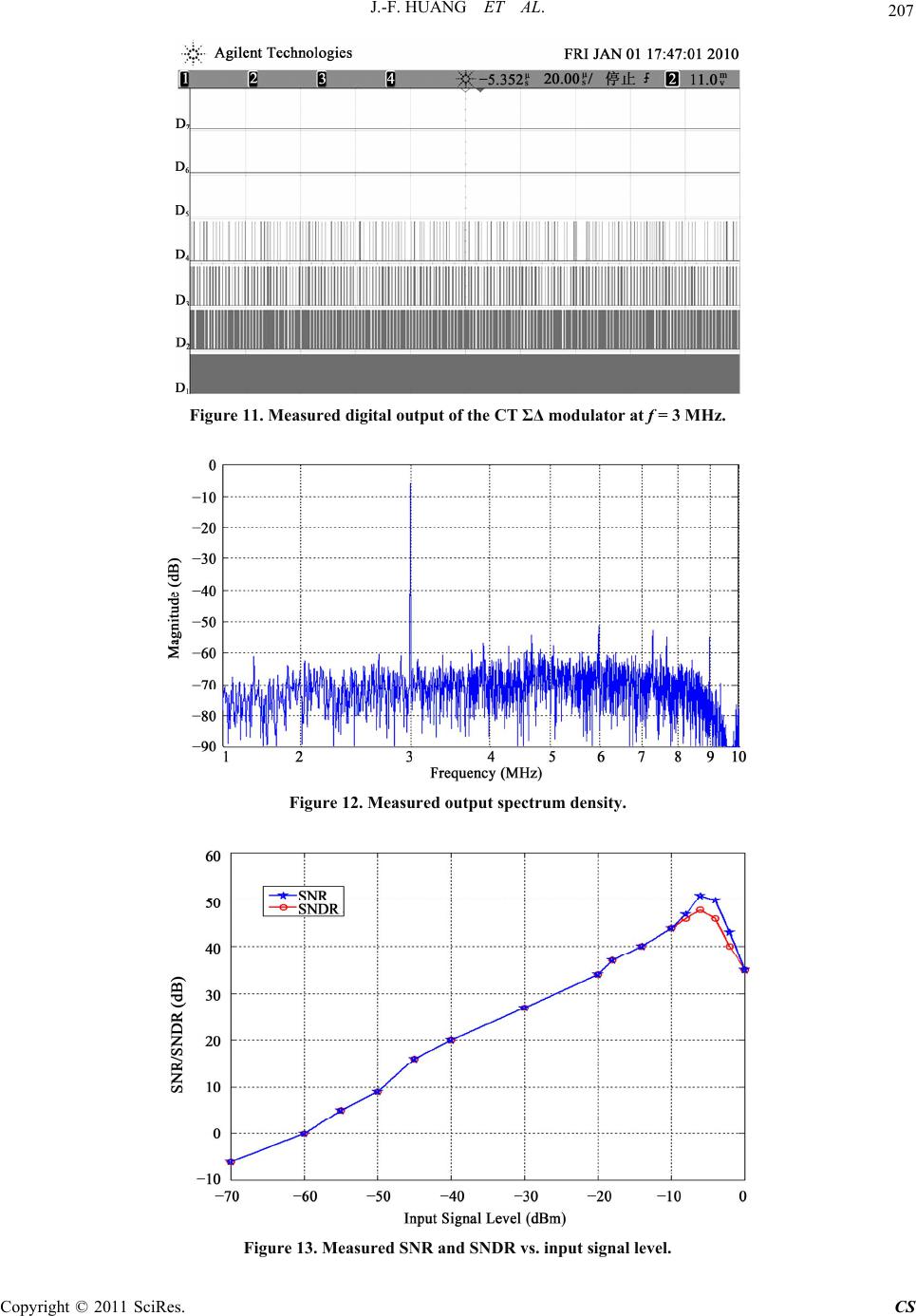 J.-F. HUANG ET AL. 207 Figure 11. Measured digital output of the CT ΣΔ modulator at f = 3 MHz. Figure 12. Measured output spectrum density. Figure 13. Measured SNR and SNDR vs. input signal level. Copyright © 2011 SciRes. CS 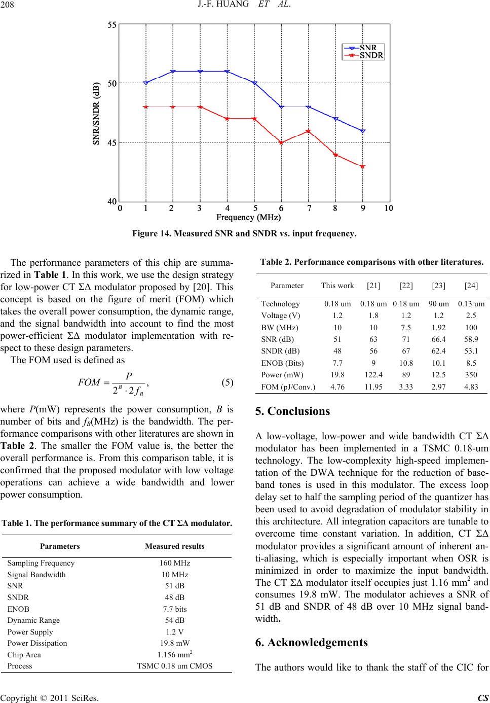 208 J.-F. HUANG ET AL. Figure 14. Measured SNR and SNDR vs. input frequency. The performance parameters of this chip are summa- riz Table 2. Performance comparisons with other literatures. ed in Table 1. In this work, we use the design strategy for low-power CT ΣΔ modulator proposed by [20]. This concept is based on the figure of merit (FOM) which takes the overall power consumption, the dynamic range, and the signal bandwidth into account to find the most power-efficient ΣΔ modulator implementation with re- spect to these design parameters. The FOM used is defined as , 22 B B P FOM f (5) where P(mW) represents the power consumption, B is able 1. The performance summary of the CT ΣΔ modulator. Parameters Measured results number of bits and fB(MHz) is the bandwidth. The per- formance comparisons with other literatures are shown in Table 2. The smaller the FOM value is, the better the overall performance is. From this comparison table, it is confirmed that the proposed modulator with low voltage operations can achieve a wide bandwidth and lower power consumption. T Sampling Frequency 160 MHz Signal Bandwidth 10 MHz SNR 51 dB SNDR Parameter This work[21] [22] [23] [24] Te0. 0. 0.chnology 0.18 um18 um18 um90 um13 um Voltage s) 1 .)1 (V) 1.2 1.8 1.2 1.2 2.5 BW (MHz) 10 10 7.5 1.92 100 SNR (dB) 51 63 71 66.4 58.9 SNDR (dB) 48 56 67 62.4 53.1 ENOB (Bit7.7 9 10.8 10.1 8.5 Power (mW) 19.8 22.4 89 12.5 350 FOM (pJ/Conv4.76 1.953.33 2.97 4.83 c Range ion 1 TSMOS 48 dB ENOB 7.7 bits Dynami54 dB Power Supply 1.2 V Power Dissipat9.8 mW Chip Area 1.156 mm2 Process C 0.18 um CM ns -power and wide bandwidth CT ΣΔ odulator has been implemented in a TSMC 0.18-um nowledgements ank the staff of the CIC for 5 . Conclusio A low-voltage, low m technology. The low-complexity high-speed implemen- tation of the DWA technique for the reduction of base- band tones is used in this modulator. The excess loop delay set to half the sampling period of the quantizer has been used to avoid degradation of modulator stability in this architecture. All integration capacitors are tunable to overcome time constant variation. In addition, CT ΣΔ modulator provides a significant amount of inherent an- ti-aliasing, which is especially important when OSR is minimized in order to maximize the input bandwidth. The CT ΣΔ modulator itself occupies just 1.16 mm2 and consumes 19.8 mW. The modulator achieves a SNR of 51 dB and SNDR of 48 dB over 10 MHz signal band- width. 6. Ack The authors would like to th Copyright © 2011 SciRes. CS  J.-F. HUANG ET AL. 209 e chip fabrication and technical supports with . Zhao, “Continuous-Time Sigma-Delta Modulator Design for Low Power Communication oermund, “A 3.3-mW ΣΔ Modulator for th the number of T18-98D-158. 7. References [1] J. Yu and B Ap- plications,” Proceedings of IEEE ASICON, October 2007, pp. 715-720. [2] R. H. M. van Veldhoven, B. J. Minnis, H. A. Hegt and A. H. M. van R UMTS in 0.18-um CMOS with 70-dB Dynamic Range in 2-MHz Bandwidth,” IEEE Journal of Solid-State Circuits, Vol. 37, No. 12, 2002, pp. 1645-1652. doi:10.1109/JSSC.2002.804329 [3] L. Dorrer, F. Kuttner, P. Greco, P. Tor “A 3-mW 74-dB SNR 2-MHz ta and T. Hartig Continuous-Time D , elta- sigma ADC with a Tracking ADC Quantizer in 0.13-um CMOS,” IEEE Journal of Solid-State Circuits, Vol. 40, No. 12, 2005, pp. 2416-2427. doi:10.1109/JSSC.2005.856282 [4] S. R. Norsworthy, R. Schreier ta-Sigma Data Converters: Theo and G. C. Temes, “Del- ry, Design and Simula- eless Applications,” a Pipeline tion,” IEEE Press, New York, 1996. [5] B. J. Farahani and M. Ismail, “Adaptive Sigma Delta ADC for WiMAX Fixed Point Wir IEEE Midwest Symposium on Circuits and Systems, Vol. 1, Covington, 7-10 August 2005, pp. 692-695. [6] T. L. Brooks, D. H. Robertson, D. F. Kelly, A. D. Muro and S. W. Harston, “A Cascaded Sigma-Delt A/D Converter with 1.25 MHz Signal Bandwidth and 89 dB SNR,” IEEE Journal of Solid-State Circuits, Vol. 32, No. 12, 1997, pp. 1896-1906. doi:10.1109/4.643648 [7] R. Jiang and T. Fiez, “A 14-bit Delta-Sigma ADC with 8X OSR and 4-MHz Conversion Bandwidth in A 0.18 um CMOS Process,” IEEE Journal of Solid-State Circuits, Vol. 39, No. 1, 2004, pp. 63-74. doi:10.1109/JSSC.2003.820877 [8] A. Bosi, A. Panigada, G. Cesura 80 MHz 4x Oversampled Cascaded and R. Castello, “An ΔΣ-Pipelined ADC In- ators for High-Speed A/D Conver- ara, “A 70-mW 300 with 75 dB DR and 87 dB SFDR,” IEEE International Solid-State Circuits Conference, 2005, pp. 174-175. [9] F. Munoz, K. Philips and A. Torralba, “A 4.7 mW 89.5 dB DR CT Complex DS ADC with Built-In LPF,” IEEE ternational Solid-State Circuits Conference, February 2005, pp. 500-501. [10] J. A. Cherry and W. M. Snelgrove, “Continuous-Time Delta-Sigma Modul sion,” Kluwer, Boston, 2000. [11] S. Paton, A. D. Giandomenico, L. Hernandez, A. Wies- bauer, T. Potscher and M. Cl-MHz CMOS Continuous-Time ΣΔ ADC with 15-MHz Band- width and 11 Bits of Resolution,” IEEE Journal of Sol- id-State Circuits, Vol. 39, No. 7, July 2004, pp. 1056- 1063. doi:10.1109/JSSC.2004.829925 [12] G. Mitteregger, C. Ebner. S. Mechnig, T. Blon, C. Holu- igue and E. Romani, “A 20-mW 640-MHz C tinuous-Time ΣΔ ADC with 20-MHz Signal Band- width, 80-dB Dynamic Range and 12-Bit ENOB,” IEEE Journal of Solid-State Circuits, Vol. 41, No. 12, 2006, pp. 2641-2649. doi:10.1109/JSSC.2006.884332 [13] S. Karthikeyan, S. Mortezapour, A. Tammineedi and E. Lee, “Low-Voltage Analog Circuit Design Based on Bi- ased Inverting Opamp Configuration,” IEEE Transac- tions on Circuits and Systems II: Analog and Digital Signal Processing, Vol. 47, No. 3, 2000, pp. 176-184. doi:10.1109/82.826743 [14] L. Lamarre, M. Louerat and A. Kaiser, “A Simple 3.8 mW 300 MHz, 4-Bit Flash A , nalog-to-Digital Converter,” Pro- ceedings of the SPIE, Vol. 5837, No. 51, 2005, pp. 825- 832. doi:10.1117/12.608343 [15] B. Razavi, “Principles of Data Conversion System De- sign,” IEEE Press, New York, 1995. ed Comparator for [16] J. Chen, S. Kurachi, S. Shen, H. Liu, T. Yoshimasu and Y. Suh, “A Low-Kickback-Noise Latch High-Speed Flash Analog-to-Digital Converters,” Inter- national Symposium on Communications and Information Technologies, Beijing, 12-14 October 2005, pp. 250-253. [17] Z. Li and T. S. Fiez, “A 14-Bit Continuous-Time Delta- sigma A/D Modulator with 2.5 MHz Signal Bandwidth,” IEEE Journal of Solid-State Circuits, Vol. 42, No. 9, 2007, pp. 1873-1883. doi:10.1109/JSSC.2007.903086 [18] J. Bastos, A. M. Marques, M. S. J. Steyaert and W. San- sen, “A 12-Bit Intrinsic Accuracy High-Speed CMOS DAC,” IEEE Journal of Solid-State Circuits, Vol. 33, No. 12, 1998, pp. 1959-1969. doi:10.1109/4.735536 [19] T. H. Kuo, K. D. Chen and H. R. Yeng, “A Wideband CMOS Sigma-Delta Modulator with Incremental Data Weighted Averaging,” IEEE Journal of Solid-State Cir- cuits, Vol. 37, No. 1, 2002, pp. 11-17. doi:10.1109/4.974541 [20] F. Gerfers, M. Ortmanns and Y. Manoli Power-Efficient Contin , “A 1.5-V 12-Bit uous-Time Third-Order ΣΔ Mod- ulator,” IEEE Journal of Solid-State Circuits, Vol. 38, No. 8, 2003, pp. 1343-1352. doi:10.1109/JSSC.2003.814432 [21] L. J. Breems, R. Rutten and G. Wetzker, “A Cascaded Continuous-Time ΣΔ Modulator with 67-dB Dynamic Range in 10-MHz Bandwidth,” IEEE Journal of Sol- id-State Circuits, Vol. 39, No. 12, 2004, pp. 2152-2160. doi:10.1109/JSSC.2004.836245 [22] S. D. Kulchycki, R. Trofin, K. Vleugels and B. A. Woo- ley, “A 77-dB Dynamic Range, 7.5-MHz Hybrid Con- tinuous-Time/Discrete-Time Cascaded ΣΔ Modulator,” IEEE Journal of Solid-State Circuits, Vol. 43, No. 4, 2008, pp. 796-804. doi:10.1109/JSSC.2008.917499 [23] M. Anderson and L. Sundstrom, “Design and Measure- ment of a CT ΔΣ ADC with Switched-Capacitor Switched- Resistor Feedback,” IEEE Journal of Solid-State Circuits, Vol. 44, No. 2, 2009, pp. 473-483. doi:10.1109/JSSC.2008.2010978 [24] A. Hart and S. P. Voinigescu, “A 1 GHz Bandwidth Low- Pass ΔΣ ADC with 20-50 GHz Adjustable Sampling Rate,” IEEE Journal of Solid- State Circuits, Vol. 44, No. 5, 2009, pp. 1401-1414. doi:10.1109/JSSC.2009.2015852 MOS Con- Copyright © 2011 SciRes. CS |