

Paper Menu >>
Journal Menu >>
 Journal of Surface Engineered Materials and Advanced Technology, 2011, 1, 35-41 doi:10.4236/jsemat.2011.12006 Published Online July 2011 (http://www.SciRP.org/journal/jsemat) Copyright © 2011 SciRes. JSEMAT 35 Effect of Annealing on Structural, Morphological, Electrical and Optical Studies of Nickel Oxide Thin Films Vik as P at il1*, Shailesh P awar1, Manik Chougule1, Prasad Godse1, Ratnakar Sakhare1, Sh as hwat i Se n2, Pradeep Joshi1 1Materials Research Laboratory, School of Physical Sciences, Solapur University, Solapur, India; 2Crystal Technology Section, Bhabha atomic Research Centre, Mumbai, I ndia. Email: [email protected] Received March 28th, 2011; revised May 3rd, 2011; accepted May 13th, 2011. ABSTRACT Sol gel spin coating method has been successfully employed for the deposition of nanocrystalline nickel oxide (NiO) thin films. The films were annealed at 400˚C - 700˚C for 1 h in an air and changes in the structural, morphological, electrical and optical properties were studied. The structural properties of nickel oxide films were studied by means of X-ray diffraction (XRD) and scanning electron microscopy (SEM). XRD analysis shows that all the films are crystal- lized in the cubic phase and present a random orientation. Surface morphology of the nickel oxide film consists of na- nocrystalline grains with uniform coverage of the substrate surface with randomly oriented morphology. The electrical conductivity showed the semiconducting nature with room temperature electrical conductivity increased from 10-4 to 10−2 (Ωcm)−1 after annealing. The decrease in the band gap energy from 3.86 to 3.47 eV was observed after annealing NiO films from 400˚C - 700˚C. These mean that the optica l qu ality of NiO films is impro v e d by annealing. Keywords: Nickel Oxide, Sol Gel Method, Structural Properties, Optoelectronic Prop erties 1. Introduction Metal oxides can adopt a large variety of structural geo- metries with an electronic structure that may exhibit me- tallic, semiconductor, or insulator characteristics, en- do wing t hem with d iverse chemical and physical proper- ties. Therefore, metal oxides are the most important functional materials used for chemical and biological sensing and transduction. Moreover, their unique and tunable physical properties have made themselves excel- lent candidates for electronic and optoelectronic applica- tions. Nanostructured metal oxides have been actively studied due to both scientific interests and potential ap- plications [1,2]. NiO is an important antifromagnetic p-type semicon- ducto r with exc ellent p roper ties suc h as gas-se nsing, c at- alytic and electrochemical properties, and has been stu- died widely for applications in solid-state sensors, elec- trochromic devices and heterogeneous catalysts as well as lithium batter ies. The nickel oxide thin films have been prepared using various techniques including ther- mal evaporation [3], spray pyrolysis [4], chemical vapor deposition [5], electrochemical deposition [6], sol-gel [7,8], sputtering [9-11], chemical solution deposition [12-16], etc. Among these, chemical solution deposition, also called as a chemical bath deposition, is an advanta- geous technique due to its low cost, low-temperature operating condition and freedom to deposit materials on a variety of substances. Verkey and Fort [14] deposited nicke l oxide t hin fil ms using ni ckel sul fate and ammonia soluti on over the temp erature range 3 30 - 350 K. Prama- nik and Bhattacharya [12] prepared nickel oxide thin films from an aqueous solution composed of nickel sul- fate, potassium persulfate, and ammonia atroom temper- ature. Han et al. [15 ] studi ed gro wth mec hani sm of ni ck- el oxide thin films following Pramanik’s chemistry. Ba- nerjee et al. [16] obtained hexagonal mesoporous nickel oxide using dodecyl sulfate as a surfactant and urea as a hydrolyzing agent. To the best of our knowledge, few works are available in the literature o n the sol-gel synthesis and characteriza- tion of NiO-based nanosystems [ 7,8]. 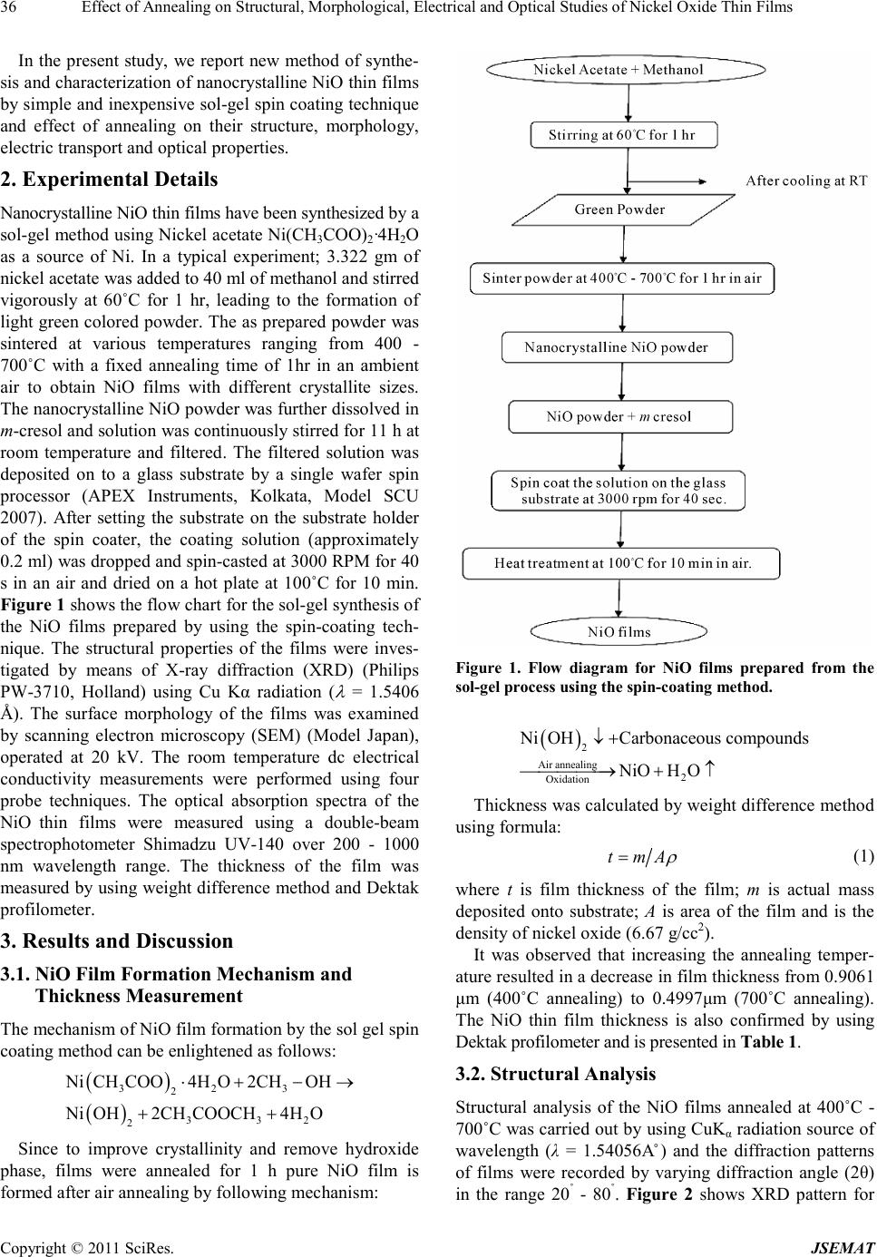 Ef fect of Annealing on Structural, Morphological, Electrical and Optical Studies of Nickel Oxide Thin Fil ms Copyright © 2011 SciRes. JSEMAT 36 In the present study, we report new method of synthe- sis and characterization of nanocrystalline NiO thin films by si mple and inexpe nsive sol-ge l spin c oatin g techniq ue and effect of annealing on their structure, morphology, electric transport and optic a l proper tie s. 2. Experimental Details Nanocrystalline NiO t hin films have been synthesized by a sol-gel method using Nickel a cetate Ni(CH3COO)2·4H2O as a source of Ni. In a typical experiment; 3.322 gm of nickel acetate was added to 40 ml of methanol and stirred vigorously at 60˚C for 1 hr, leading to the formation of light green colored po wder. The as prepared powder was sintered at various temperatures ranging from 400 - 700˚C with a fixed annealing time of 1hr in an ambient air to obtain NiO films with different crystallite sizes. The nanoc rysta lli ne NiO powde r was furt her di ssolved in m-cresol and s ol ution was c ontinuously stirred for 11 h at room temperature and filtered. The filtered solution was deposited on to a glass substrate by a single wafer spin processor (APEX Instruments, Kolkata, Model SCU 2007). After setting the substrate on the substrate holder of the spin coater, the coating solution (approximately 0.2 ml) was dropped and spin-casted at 3000 RPM for 40 s in an air and dried on a hot plate at 100˚C for 10 min. Figure 1 shows the f low char t fo r t he so l -gel s ynthe s is o f the NiO films prepared by using the spin-coating tech- nique. The structural properties of the films were inves- tigated by means of X-ray diffraction (XRD) (Philips PW-3710, Holland) using Cu Kα radiation ( λ = 1.5406 Å). The surface morphology of the films was examined by scanning electron microscopy (SEM) (Model Japan), operated at 20 kV. The room temperature dc electrical conductivity measurements were performed using four probe techniques. The optical absorption spectra of the NiO thin films were measured using a double-beam spectrophotometer Shimadzu UV-140 over 200 - 1000 nm wavelength range. The thickness of the film was measured by using weight difference method and Dektak profilometer. 3. Results and Discussion 3.1. NiO Film Formation Mechanism and Thickness Measurement The mechanism of NiO film formation by the sol gel spin coating method can be enlightened as follows: ( ) ( ) 3 23 2 3 32 2 NiCH COO4HO2CHOH NiOH2CH COOCH4HO ⋅ + −→ ++ Since to improve crystallinity and remove hydroxide phase, films were annealed for 1 h pure NiO film is formed after air annealing by follo wing me c hanism: Figure 1. Flow diagram for NiO films prepared from the sol-g el pro cess using the spin-coating method. ( ) 2 Air annealing2 Oxidation NiOHCarbonaceous compounds NiOH O ↓+ → +↑ Thickness was calculated by weight difference method using formula: t mA ρ = (1) where t is film thickness of the film; m is actual mass deposited onto substrate; A is area of the film and is the densi ty of nickel oxide (6.67 g/cc2). It was observed that increasing the annealing temper- ature resulted in a decrease in film thickness from 0.906 1 μm (400˚C annealing) to 0.4997μm (700˚C annealing). The NiO thin film thickness is also confirmed by using Dektak profilometer and is presented in Table 1. 3.2. Structural Analysis Structural analysis of the NiO films annealed at 400˚C - 700˚C was carri ed out b y usi ng CuK α radiation source of wavelength (λ = 1.54056A˚) and the diffraction patterns of films were recorded by varying diffraction angle (2θ) in the range 20˚ - 80˚. Fig ur e 2 shows XRD pattern for 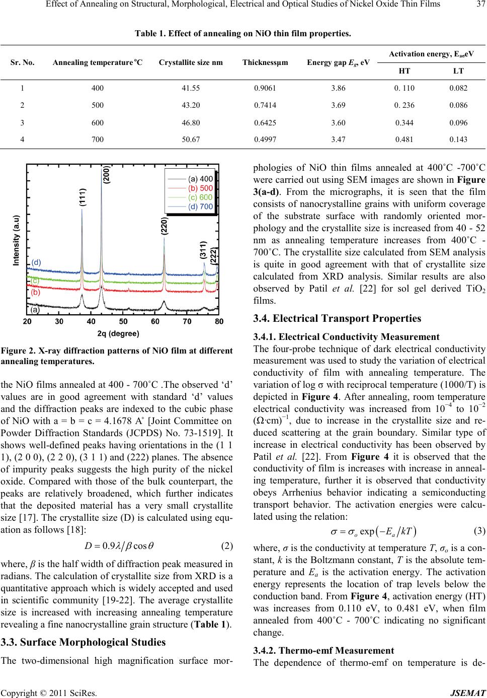 Ef fect of Annealing on Structural, Morphological, Electrical and Optical Studies of Nickel Oxide Thin Fil ms Copyright © 2011 SciRes. JSEMAT 37 Table 1. Effect of annealing on NiO thin film properties. Sr. No. Annealing temperature oC Crystallite size nm Thicknessμm Ene rg y gap Eg, eV Activ at i on en er g y, EaσeV HT LT 1 400 41.55 0.9061 3.86 0. 1 10 0.082 2 500 43.20 0.7414 3.69 0. 2 36 0.086 3 600 46.80 0.6425 3.60 0.344 0.096 4 700 50.67 0.4997 3.47 0.481 0.143 Figure 2. X-ray diffraction patterns of NiO film at different annealing te mp eratures. the NiO films annealed at 400 - 700˚C .The observed ‘d’ values are in good agreement with standard ‘d’ values and the diffraction peaks are indexed to the cubic phase of NiO with a = b = c = 4.1678 A˚ [Joint Committee on Powder Diffraction Standards (JCPDS) No. 73-1519]. It shows well-defined peaks having orie ntations in the (1 1 1), (2 0 0), (2 2 0), (3 1 1) and (222) planes. The absence of impurity peaks suggests the high purity of the nickel oxide. Compared with those of the bulk counterpart, the peaks are relatively broadened, which further indicates that the deposited material has a very small crystallite size [17]. The crystallite size (D) is calculated using equ- ation as follows [18]: 0.9 cosD λβ θ = (2) where, β is the half width of diffraction peak measured in radians. The calculation of crystallite size from XRD is a quantitative approach which is widely accepted and used in scientific community [19-22]. The average crystallite size is increased with increasing annealing temperature revealing a fine nanocrystalline grain structure (Table 1). 3.3. Surface Morphological Studies The two-dimensional high magnification surface mor- phologies of NiO thin films annealed at 400˚C -700˚C were carried out using SEM images are s hown in F igure 3(a-d). From the micrographs, it is seen that the film consists of nanocrystalline grains with uniform coverage of the substrate surface with randomly oriented mor- phology and the cr ystallite size is increased from 40 - 52 nm as annealing temperature increases from 400˚C - 700˚C. The crystallite size calculated from SEM analysis is quite in good agreement with that of crystallite size calculated from XRD analysis. Similar results are also observed by Patil et al. [22] for sol gel derived TiO2 fil ms . 3.4. Electrical Transport Properties 3.4.1. Electrical Conductivity Measurement The four-probe technique of dark electrical conductivity measurement was used to study the variation of electrical conductivity of film with annealing temperature. The variation of log σ with reciprocal temperature (1000/T) is depicted in Figure 4. After annealing, room temperature electrical conductivity was increased from 10−4 to 10−2 (Ω·cm)−1, due to increase in the crystallite size and re- duced scattering at the grain boundary. Similar type of increase in electrical conductivity has been observed by Patil et al. [22]. From Figure 4 it is observed that the conductivity of film is increases with increase in anneal- ing temperature, further it is observed that conductivity obeys Arrhenius behavior indicating a semiconducting transport behavior. The activation energies were calcu- late d using the r elation: ( ) exp oa E kT σσ = − (3) where, σ is the conductivity at temperature T, σo is a con- stant, k is the Boltzmann constant, T is the absolute tem- perature and Ea is the activation energy. The activation energy represents the location of trap levels below the conduction band. From Figure 4, activatio n energy (HT ) was increases from 0.110 eV, to 0.481 eV, when film annealed from 400˚C - 700˚C indicating no significant change. 3.4.2. Thermo-emf Measurement The dependence of thermo-emf on temperature is de- 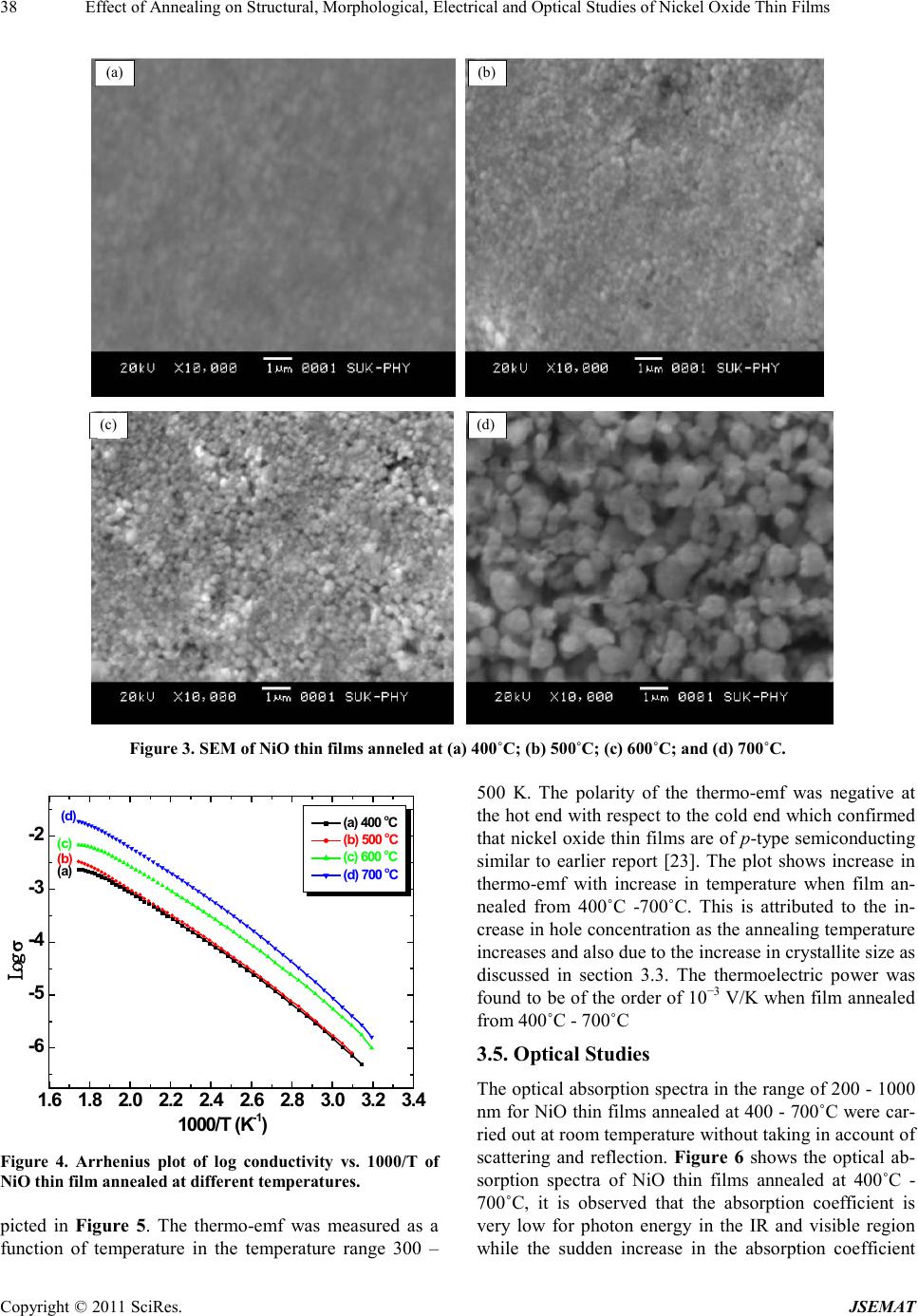 Ef fect of Annealing on Structural, Morphological, Electrical and Optical Studies of Nickel Oxide Thin Fil ms Copyright © 2011 SciRes. JSEMAT 38 (a) (b) (d) (c) Figure 3. S EM of N iO thin films annel ed at (a) 400˚C; (b) 500˚C; (c) 600˚C; and (d) 700˚C. 1.6 1.8 2.0 2.2 2.4 2.6 2.83.0 3.2 3.4 -6 -5 -4 -3 -2 (a) (b) (c) (d) Log σ 1000/T (K -1 ) (a) 400 o C (b) 500 o C (c) 600 o C (d) 700 o C Figure 4. Arrhenius plot of log conductivity vs. 1000/T of NiO thin film anneal ed at different temperatures. picted in Figure 5. The thermo-emf was measured as a function of temperature in the temperature range 300 – 500 K. The polarity of the thermo-emf was negative at the hot end wit h respe ct to t he co ld end whic h confirmed that nickel oxid e thin films are of p-t ype s em iconducting similar to earlier report [23]. The plot shows increase in th ermo-emf with increase in temperature when film an- nealed from 400˚C -700˚C. This is attributed to the in- crease in hole concentration as the annealing temperature increases and also due to the increase in crystallite size as discussed in section 3.3. The thermoelectric power was found to be of the order of 10−3 V/K when film annealed from 400˚C - 700˚C 3.5. Optical Studies The optical absorption spectra in the range of 200 - 1000 nm for NiO thin films annealed at 400 - 700˚C were car- ried out at room temperature witho ut t a kin g i n a cc o u nt of scattering and reflection. Figure 6 shows the optical ab- sorption spectra of NiO thin films annealed at 400˚C - 700˚C, it is observed that the absorption coefficient is very low for photon energy in the IR and visible region while the sudden increase in the absorption coefficient 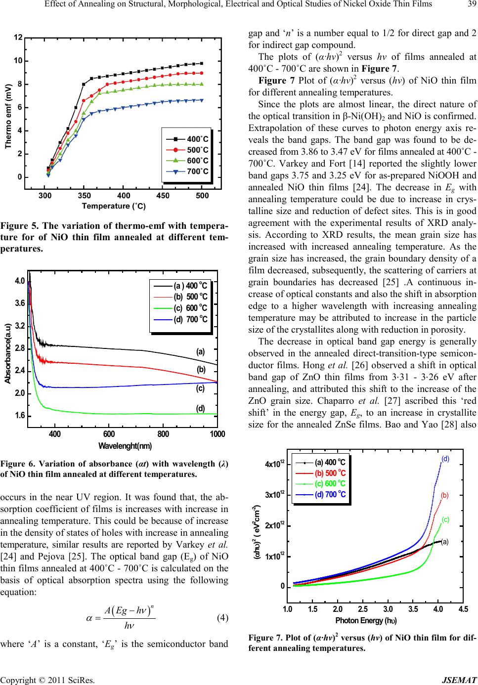 Ef fect of Annealing on Structural, Morphological, Electrical and Optical Studies of Nickel Oxide Thin Fil ms Copyright © 2011 SciRes. JSEMAT 39 Figure 5. The variation of thermo-emf with tempera- ture for of NiO thin film annealed at different tem- peratures. 400600800 1000 1. 6 2. 0 2. 4 2. 8 3. 2 3. 6 4. 0 ( d) (c) ( b) (a) Absorbanc e(a.u) Wavelenght(nm) (a ) 400 o C (b) 500 o C (c) 600 o C (d) 700 o C Figure 6. Variation of absorbance (αt) with wavelength (λ) of NiO thin f ilm annealed at different temperatures. occurs in the near UV region. It was found that, the ab- sorption coefficient of films is increases with increase in annealing temperature. This could be because of increase in the density of states of holes with increa s e in annealing temperature, similar results are reported by Varkey et al. [24] and Pejova [25]. The optical band gap (Eg) of NiO thin fil ms annea led at 4 00˚C - 700˚C is calculated on the basis of optical absorption spectra using the following equation: ( ) n A Egh h ν αν − = (4) where ‘A’ is a constant, ‘Eg’ is the semiconductor band gap a nd ‘n’ is a number equal to 1/2 for direct gap and 2 for indirect gap compound. The plots of (α·hν)2 versus hν of films annealed at 400˚C - 700˚C are s hown in Figure 7. Figure 7 Plot of (α·hν)2 versus (hv) of NiO thin film for different annealing temperatures. Since the plots are almost linear, the direct nature of the optical transition in β-Ni(OH)2 and NiO is co nfir med. Extrapolation of these curves to photon energy axis re- veals the band gaps. The band gap was found to be de- creased from 3.86 to 3.47 eV for films annealed at 400˚C - 700˚C. Varkey and Fort [14] reported the slightly lower band gaps 3.75 and 3.25 eV for as-prepared NiOOH and annealed NiO thin films [24]. The decrease in Eg with annealing temperature could be due to increase in crys- talline size and reduction of defect sites. This is in good agreement with the experimental results of XRD analy- sis. According to XRD results, the mean grain size has increased with increased annealing temperature. As the grain size has increased, the grain boundary density of a film decreased, subsequently, the scattering of carriers a t grain boundaries has decreased [25] .A continuous in- crease of optical constants and also the shift in absorption edge to a higher wavelength with increasing annealing temperature may be attributed to increase in the particle size of the crystal lite s along with red uction in por os i ty. The decrease in optical band gap energy is generally observed in the annealed direct-transition-type semicon- ductor films. Hong et al. [26] observed a shift in optical band gap of ZnO thin films from 3⋅31 - 3⋅26 eV after annealing, and attributed this shift to the increase of the ZnO grain size. Chaparro et al. [27] ascribed this ‘red shift’ in the energy gap, Eg, to an increase in crystallite size for the annealed ZnSe films. Bao and Yao [28] also 1.0 1.5 2.0 2.5 3.0 3.5 4.0 4.5 0 1x10 12 2x10 12 3x10 12 4x10 12 (d) (c) (b) (a) (αhυ) 2 ( eV 2 cm -2 ) Photon Energy (hυ) (a) 400 o C (b) 500 o C (c) 600 o C (d) 700 o C Figure 7. P lot of (α· h ν)2 versus (h v) of NiO t hin fi lm for dif- ferent ann eal ing temperatures. 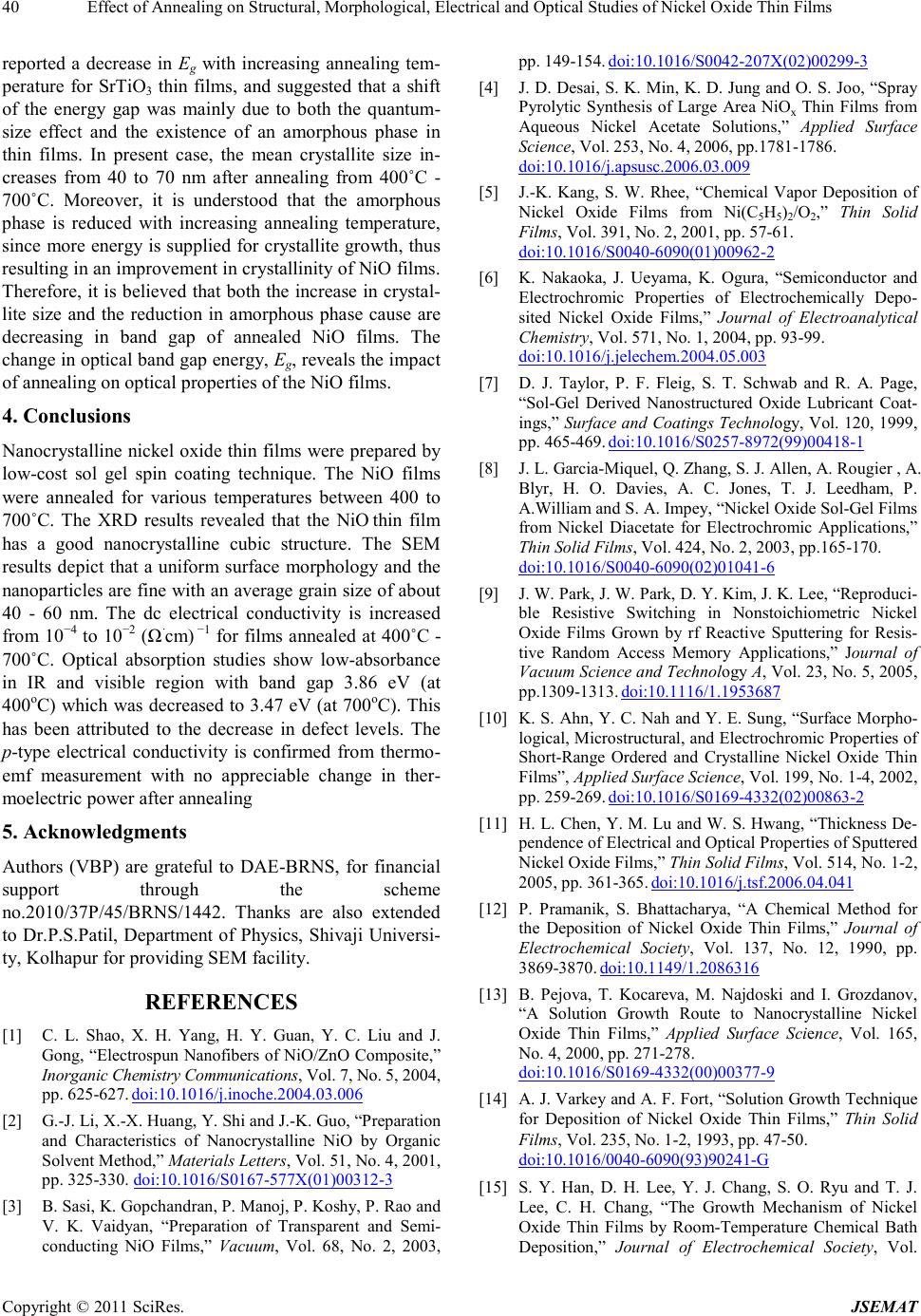 Ef fect of Annealing on Structural, Morphological, Electrical and Optical Studies of Nickel Oxide Thin Fil ms Copyright © 2011 SciRes. JSEMAT 40 reported a decrease in Eg with increasing annealing tem- perature for SrTiO3 thin films, and suggested that a shift of the energy gap was mainly due to both the quantum- size effect and the existence of an amorphous phase in thin films. In present case, the mean crystallite size in- creases from 40 to 70 nm after annealing from 400˚C - 700˚C. Moreover, it is understood that the amorphous phase is reduced with increasing annealing temperature, since more energ y is supplied for cr ystallite growth, thus resul ti n g i n an i mpr o ve me nt i n crysta llinit y o f N iO fi l ms . Therefore, it is believed that both the increase in crystal- lite size and the reduction in amorphous phase cause are decreasing in band gap of annealed NiO films. The change in optical band gap energy, Eg, reveals the impact of annealing on optical properties of the NiO films. 4. Conclusions Nanocrystalline nickel oxide thin films were prepared by low-cost sol gel spin coating technique. The NiO films were annealed for various temperatures between 400 to 700˚C. The XRD results revealed that the NiO thin film has a good nanocrystalline cubic structure. The SEM results depict that a uniform surface morphology and the nanopar ticles are fine with an average grain size of about 40 - 60 nm. The dc electrical conductivity is increased fro m 10−4 to 10−2 (Ω·cm) −1 for films annealed at 400˚C - 700˚C. Optical absorption studies show low-absorbance in IR and visible region with band gap 3.86 eV (at 400oC) which was decreased to 3.47 eV (at 700oC). T his has been attributed to the decrease in defect levels. The p-type electrical conductivity is confirmed from thermo- emf measurement with no appreciable change in ther- moelectric power after a nnealing 5. Acknowledgments Authors (VBP) are grateful to DAE-BRNS, for financial support through the scheme no.2010/37P/45/BRNS/1442. Thanks are also extended to Dr.P.S.Patil, Department of Physics, Shivaji Universi- ty, Kolhapur fo r providi ng S EM fa cility. REFERENCES [1] C. L. Shao, X. H. Yang, H. Y. Guan, Y. C. Liu and J. Gong, “Electrospun Nanofibers of NiO/ZnO Composite,” Inorganic Chemistry Communications, Vol. 7, No. 5, 2004, pp. 625-627. doi:10.1016/j.inoche.2004.03.006 [2] G.-J. Li , X .-X. Huang, Y. Shi and J.-K. Guo, “Preparation and Charact er istics of Nanocrystalline NiO by Organic Solvent Method,” Materials Letters, Vol. 51 , No . 4, 2001, pp. 325-330. doi:10.1016/S0167-577X(01)00312-3 [3] B. Sasi, K. Gopchandran, P. Manoj, P. Koshy, P. Rao and V. K. Vaidyan, “Preparation of Transparent and Semi- conducting NiO Films,” Vacuum, Vol. 68, No. 2, 2003, pp. 149-154. doi:10.1016/S0042-207X(02)00299-3 [4] J. D. Desai, S. K. Min, K. D. Ju ng and O. S. Joo, “Spray Pyrolytic Synthesis of Large Area NiOx Thin Films from Aqueous Nickel Acetate Solutions,” Applied Surface Scien ce, Vol. 253, No. 4, 2006, pp.1781-1786. doi:10.1016/j.apsusc.2006.03.009 [5] J.-K. Kang, S. W. Rhee, “Chemical Vapor Deposition of Nickel Oxide Films from Ni(C5H5)2/O2,” Thin Solid Films, Vol. 391, No. 2, 20 01 , pp. 57-61. doi:10.1016/S0040-6090(01)00962-2 [6] K. Nakaoka, J. Ueyama, K. Ogura, “Semiconductor and Electrochromic Properties of Electrochemically Depo- sited Nickel Oxide Films,” Journal of Electroanalytical Chemistry, Vol. 571, No. 1, 2004, pp. 93-99. doi:10.1016/j.jelechem.2004.05.003 [7] D. J. Taylor, P. F. Fleig, S. T. Schwab and R. A. Page, “Sol-Ge l Derived Nanostructured Oxide Lubricant Coat- ings,” Surface and Coatings Technol ogy, Vol. 120, 1999, pp. 465-469. doi:10.1016/S0257-8972(99)00418-1 [8] J. L. Garcia-Miquel, Q. Zhang, S. J. Allen, A. Rougier , A. Blyr, H. O. Davies, A. C. Jones, T. J. Leedham, P. A.William and S. A. Impey, “Nickel Oxide Sol-Gel Films from Nickel Diacetate for Electrochromic Applications,” Thin Solid Films, Vol. 424, No. 2, 2003, pp.165-170. doi:10.1016/S0040-6090(02)01041-6 [9] J. W. Park, J. W. Park, D. Y. Kim, J. K. Lee, “Repr od uci- ble Resistive Switching in Nonstoichiometric Nickel Oxide Films Grown by rf Reactive Sputtering for Resis- tive Random Access Memory Applications,” Journal of Vacuum Science and Technology A, V ol. 23, No . 5, 2005, pp.1309-1313. doi:10.1116/1.1953687 [10] K. S. Ahn, Y. C. Nah and Y. E. Sung, “Su rface Morpho- logical, Micro structu ral, and E lectrochr omic Prop erties of Short-Range Ordered and Crystalline Nickel Oxide Thin Films”, Applied Surface S cience, Vol. 199, No. 1 -4, 2002, pp. 259-269. doi:10.1016/S0169-4332(02)00863-2 [11] H. L. Chen, Y. M. Lu and W. S. Hwang, “Thicknes s De- pendence of Electri cal and Optical Properties of Spu ttered Nickel Oxide Films,” Thin Solid Films, Vol. 514, No. 1-2, 2005, p p. 361 -365. doi:10.1016/j.tsf.2006.04.041 [12] P. Pramanik, S. Bhattacharya, “A Chemical Method for the Deposition of Nickel Oxide Thin Films,” Journal of Electrochemical Society, Vol. 137, No. 12, 1990, pp. 3869-3870. doi:10.1149/1.2086316 [13] B. Pejova, T. Kocareva, M. Najdoski and I. Grozdanov, “A Solution Growth Route to Nanocrystalline Nickel Oxide Thin Films,” Applied Surface Scien ce, Vol. 165, No. 4, 2000, pp. 271-278. doi:10.1016/S0169-4332(00)00377-9 [14] A. J. V arke y and A. F. Fort, “Solution Growth Technique for Deposition of Nickel Oxide Thin Films,” Thin Solid Films, Vol. 235, No. 1-2, 1993, pp. 47-50. doi:10.1016/0040-6090(93)90241-G [15] S. Y. Han, D. H. Lee, Y. J. Chang, S. O. Ryu and T. J. Lee, C. H. Chang, “The Growth Mechanism of Nickel Oxide Thin Films by Room-Temperature Chemical Bath Deposition,” Journal of Electrochem ical Society, Vol. 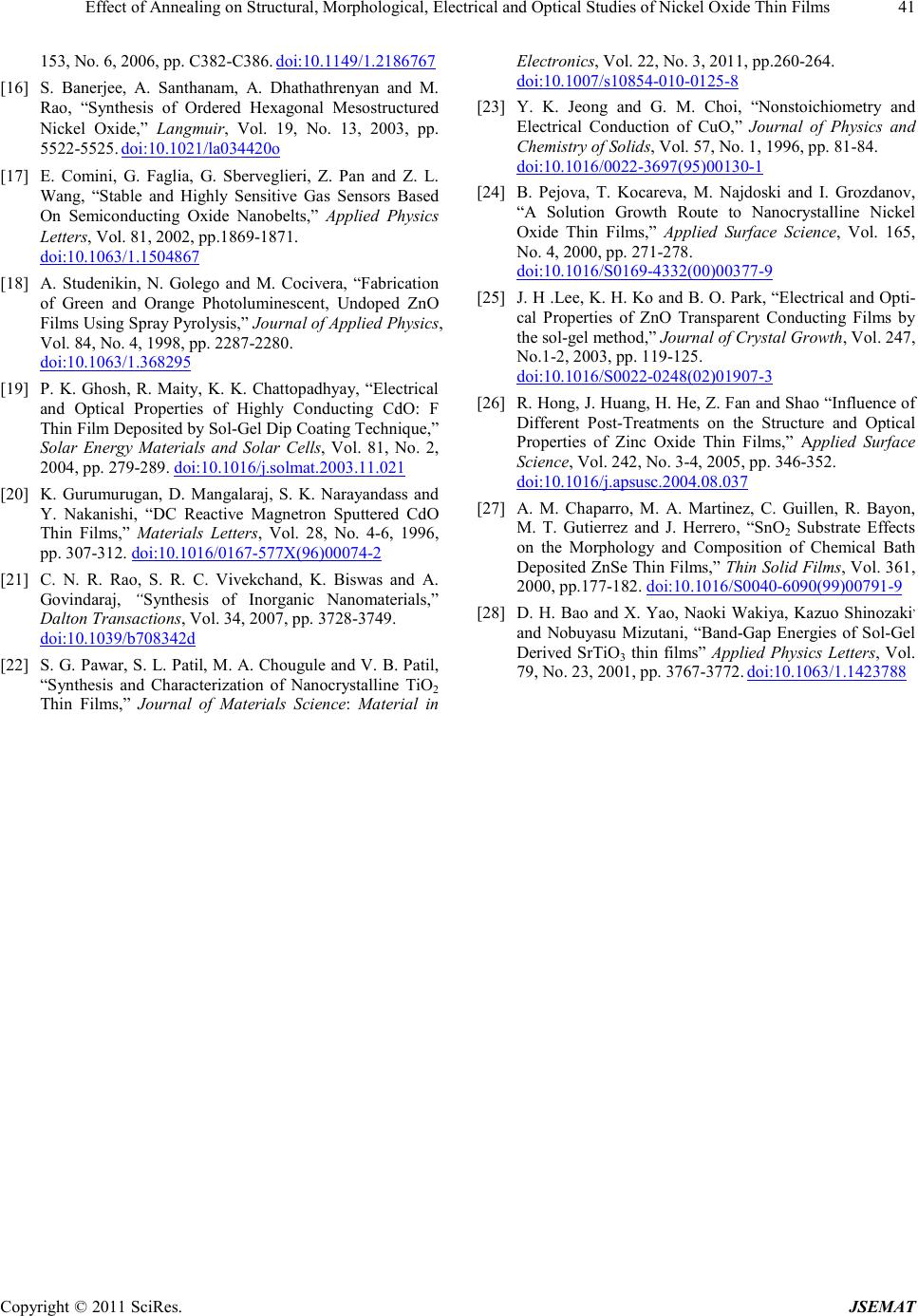 Ef fect of Annealing on Structural, Morphological, Electrical and Optical Studies of Nickel Oxide Thin Fil ms Copyright © 2011 SciRes. JSEMAT 41 153, No. 6, 2006, pp. C382-C386. doi:10.1149/1.2186767 [16] S. Banerjee, A. Santhanam, A. Dhathathrenyan and M. Rao, “Synthesis of Ordered Hexagonal Mesostructured Nickel Oxide,” Langmuir , Vol. 19, No. 13, 2003, pp. 5522-5525. doi:10.1021/la034420o [17] E. Comini, G. Faglia, G. Sberveglieri, Z. Pan and Z. L. Wang, “Stable and Highly Sensitive Gas Sensors Based On Semiconducting Oxide Nanobelts,” Applied Physics Letters, Vol. 81, 2002, pp.1869-1871. doi:10.1063/1.1504867 [18] A. Studenikin, N. Golego and M. Cocivera, “F abrication of Green and Orange Photoluminescent, Undoped ZnO Films Using Spra y Pyrol ysis,” Journal of Applied Physics, Vol. 84, No. 4, 1998, pp. 2287-2280. doi:10.1063/1.368295 [19] P. K. Ghosh, R. Maity, K. K. Chattopadhyay, “Electrical and Optical Properties of Highly Conducting CdO: F Thin Film Deposited by Sol-Gel Dip Coating Technique,” Solar Energy Materials and Solar Cells, Vol. 81, No. 2, 2004, pp . 279-289. doi:10.1016/j.solmat.2003.11.021 [20] K. Gurumurugan, D. Mangalaraj, S. K. Narayandass and Y. Nakanishi, “DC Reactive Magnetron Sputtered CdO Thin Films,” Materials Letters, Vol. 28, No. 4-6, 1996, pp. 307-312. doi:10.1016/0167-577X(96)00074-2 [21] C. N. R. Rao, S. R. C. Vivekchand, K. Biswas and A. Govindaraj, “Synthesis of Inorganic Nanomaterial s,” Dal ton Tr ansactions, Vol. 3 4, 20 07, pp. 3728-3749. doi:10.1039/b708342d [22] S. G. Pawar, S. L. Patil, M. A. Chougule and V. B. Patil, “Synthesis and Characterization of Nanocrystalline TiO2 Thin Films,” Journal of Materials Science: Material in Electronics, Vol. 22, No. 3, 2011, pp.260-264. doi:10.1007/s10854-010-0125-8 [23] Y. K. Jeong and G. M. Choi, “Nonstoichiometry and Electrical Conduction of CuO,” Journal of Physics and Chemistry of Solids, Vol. 57, No. 1, 1996, pp. 81-84. doi:10.1016/0022-3697(95)00130-1 [24] B. Pejova, T. Kocareva, M. Najdoski and I. Grozdanov, “A Solution Growth Route to Nanocrystalline Nickel Oxide Thin Films,” Applied Surface Science, Vol. 165, No. 4, 2000, pp. 271-278. doi:10.1016/S0169-4332(00)00377-9 [25] J. H .Lee, K. H. Ko and B. O. Park, “E lectrical and Opti- cal Properties of ZnO Transparent Conducting Films by the sol-gel method,” Journal of Crystal Growth, Vol. 247, No.1-2, 2003, pp. 119-125. doi:10.1016/S0022-0248(02)01907-3 [26] R. Hong, J. Huang, H. He, Z. Fan and Shao “Influence of Different Post-Treatments on the Structure and Optical Properties of Zinc Oxide Thin Films,” Applied Surface Scien ce, Vol. 242, N o. 3-4, 2005, pp. 346-352. doi:10.1016/j.apsusc.2004.08.037 [27] A. M. Chaparro, M. A. Martinez, C. Guillen, R. Bayon, M. T. Gutierrez and J. Herrero, “SnO2 Substrate Effects on the Morphology and Composition of Chemical Bath Deposited ZnSe Thin Films,” Thin Solid Films, Vol. 361, 2000, pp .177-182. doi:10.1016/S0040-6090(99)00791-9 [28] D. H. Bao and X. Yao, Naoki Wakiya, Kazuo Shinozaki, and Nobuyasu Mizutani, “Band-Gap Energies of Sol-Gel Derived SrTiO3 thin films” Applied Physics Letters, Vol. 79, No. 23, 2001, pp. 3767-3772. doi:10.1063/1.1423788 |