

Paper Menu >>
Journal Menu >>
 Circuits and Systems, 2011, 2, 237-241 doi:10.4236/cs.2011.23033 Published Online July 2011 (http://www.SciRP.org/journal/cs) Copyright © 2011 SciRes. CS Electronically Tunable Minimum Component Biquadratic Filters for Interface Circuits Mehmet Sağbaş Department of Electronics Engineering, Maltepe University, Istanbul, Turkey E-mail: [email protected] Received November 23, 2010; revised May 24, 2011; accepted June 1, 2011 Abstract In this paper, two new electronically tunable filter configurations are proposed. The proposed filters operate current-mode (CM), voltage-mode (VM), transimpedance-mode (TIM) and transadmittance-mode (TAM). The first configuration realizes second-order VM band-pass and TAM high-pass filter characteristics from the same configuration. The second one realizes second-order TIM band-pass and CM low-pass filter char- acteristics from the same configuration. They also use minimum number of electronic components (two ca- pacitors and one active component namely; current controlled current difference transconductance amplifier). The workability of the proposed structures has been demonstrated by simulation results. Keywords: Second-Order Filters, CC-CDBA, Electronic Tunability, Current-Mode Circuits, Interface Circuits 1. Introduction It is well known that current-mode and voltage-mode are still important integrated circuit (IC) operations [1-3]. Recently, there is a growing interest in transimpedance- mode and transadmittance-mode operations. A current- input voltage-output filter or voltage-input current-output filter is described as an interface circuit connecting a current-mode circuit to a voltage-mode circuit or a volt- age-mode circuit to a current-mode circuit, respectively. These interface circuits are needed in many applications where VM and CM circuits are used together. In addition, the other important application area of transadmittance- mode filters are the receiver baseband blocks of modern radio systems [4,5]. Also the outputs of the many digi- tal/analog converters (DACs) are available as current signals. Then the transimpedance-mode filters can be used for conversion of the signals at the outputs of these DACs, simultaneously. Therefore, several TAM- and TIM-type filters are proposed using different-type active components [6-12]. Simplicity, cost reduction, power consumption and versatility are all important for the integrated circuit manufacturers. Therefore, number of the components is an important parameter. Therefore, numerous circuits are proposed in literature that employing minimum number of component [13-17]. However, these filters use at least four electronic components. The proposed filter is com- pared to the other filters reported in the literature by the use of Table 1. According to Table 1, the proposed filter has advantages over the proposed filters in Ref [13-14], since it has electronically tunability property and no ex- ternal resistors. In this paper, two new second order filter configura- tions using only single active component and two ca- pacitors are presented. They realize CM, VM, TIM and TAM second order filter characteristics from the same configuration. Similar kinds of circuits in the literature use more than three elements [13-16] (see Table 1). The paper is organized as in the following sections: In the next section, after a short introduction of CC-CDBA, Table 1. Comparison of the cited references and the pro- posed filter. Ref. Active Element External Capacitor External Resistor Electronic Tunability [13] 1 CDBA2 2 No [14] 1 CDBA2 2 No [15] 1 CCII+ 2 2 No [16] 1 CCCII2 1 Yes Proposed Filter 1 CC-CDBA2 0 Yes 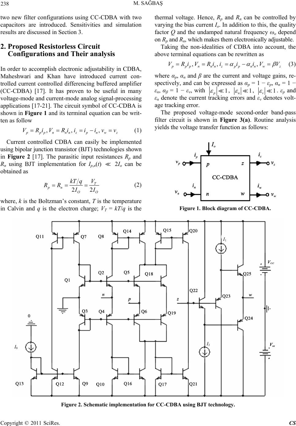 238 M. SAĞBAŞ two new filter configurations using CC-CDBA with two capacitors are introduced. Sensitivities and simulation results are discussed in Section 3. 2. Proposed Resistorless Circuit Configurations and Their analysis In order to accomplish electronic adjustability in CDBA, Maheshwari and Khan have introduced current con- trolled current controlled differencing buffered amplifier (CC-CDBA) [17]. It has proven to be useful in many voltage-mode and current-mode analog signal-processing applications [17-21]. The circuit symbol of CC-CDBA is shown in Figure 1 and its terminal equation can be writ- ten as follow ,, , p ppnnn zpnwz VRiVRiiiivv (1) Current controlled CDBA can easily be implemented using bipolar junction transistor (BJT) technologies shown in Figure 2 [17]. The parasitic input resistances Rp and Rn using BJT implementation for Ip,n(t) 2Io can be obtained as 22 T pn OO V kT q RR I I (2) where, k is the Boltzman’s constant, T is the temperature in Calvin and q is the electron charge; VT = kT/q is the thermal voltage. Hence, Rp and Rn can be controlled by varying the bias current Io. In addition to this, the quality factor Q and the undamped natural frequency ωo depend on Rp and Rn, which makes them electronically adjustable. Taking the non-idealities of CDBA into account, the above terminal equations can be rewritten as ,, , p ppnnn zppnnwz VRiVRiiiiV V (3) where αp, αn and β are the current and voltage gains, re- spectively, and can be expressed as αp = 1 − εp, αn = 1 − εn, αβ = 1 − εv, with 1 p , 1 n , 1 v . εp and εn denote the current tracking errors and εv denotes volt- age tracking error. The proposed voltage-mode second-order band-pass filter circuit is shown in Figure 3(a). Routine analysis yields the voltage transfer function as follows: Figure 1. Block diagram of CC-CDBA. I 1 I 2 I 0 Figure 2. Schematic implementation for CC-CDBA using BJT technology. Copyright © 2011 SciRes. CS  M. SAĞBAŞ Copyright © 2011 SciRes. CS 239 1 2 1212 1 out n in pnp n VsCR VsCCRRs CRCR (4) The proposed filter in shown Figure 3(a) also gives minimum component transimpedance-mode high-pass filter response. Therefore, the current output response of the proposed circuit is 2 12 2 1212 1 out n in pnp n IsCCR VsCCRRs CRCR (5) The proposed current-mode second-order band-pass filter circuit is shown in Figure 3(b). Routine analysis yields the voltage transfer function as follows: 2 2 1212 1 out n in pnp n IsCR IsCCRRs CRCR (6) It also gives minimum component TIM low-pass filter response. Therefore, the voltage output response of the proposed circuit is 2 1212 1 out n in pnp n VR IsCCRRs CRCR (7) The undamped natural frequency and the quality factor of the proposed circuit are obtained from the denomina- tor of the transfer function as follows: 12 12 12 1, p n o p n pn CC RR ωQCRC R CC RR (8) Taking the non-idealities of CC-CDBA given in Equa- tion (3) into account, the denominator polynomial of the transfer function for the proposed filters becomes 2 121 2 p nnpn DssCCRR sβαCRC Rβα n (9) Using Equation (9), non-ideal the undamped natural frequency and the quality factor becomes ,n12 pn n o 12 pnn1 p2n βα CC RR βα ω=Q= CC RRβα CR +CR (10) From Equation (10), the quality factor Q and the un- damped natural frequency ωo depend on Rp and Rn which can be controlled by varying the bias current Io. There- fore, they can be adjusted electronically. 3. Sensitivity Consideration and Simulation Results The ideal sensitivities of the natural frequency and the quality factor with respect to passive components are calculated as follows 0.5, oooo pn12 ωωωω RRCC ==== SSSS (11) 11 0.5 p QQ R C CR k SS p (12) 22 0.5 n QQ R C CRk SS n (13) where, 12 1 p n kCRCR . If the passive component values are chosen appropri- ately, the ideal sensitivities will be smaller than 1. Using Equation (10), the non-ideal sensitivities can be found as 0.5, 0 oo o n ωω ω β α = SS S p α (14) 0.5 n QQ β αn1p == βα CRk SS (15) where, 12 1np n kβα CRC R. Again, if passive component values are chosen appro- priately, the sensitivities due to non-ideal effects will also be small than 1. The performance of the filter topology given in Figure 3(a) is verified using PSpice. Each CC-CDBA is realized by its BJT implementation shown in Figure 2 with the transistor model of PR100N (PNP) and NR100N (NPN) of the bipolar arrays ALA400 from AT & T [22]. In all of the simulations, the voltage supplies of CC-CDBA are taken as Vcc = 2.5 V and Vee = –2.5 V. To confirm the obtained results with the theoretical results and demonstrate tunability property of the pro- posed configuration, the gain characteristics obtained by PSPICE for two cases are plotted in Figure 4 together. In these simulations, bias currents of CC-CDBA are Io = 10 μA and Io = 20 μA, for simulation 1 and 2, respectively. (a) (b) Figure 3. Circuit diagram of the proposed filters. (a) VM and TAM filter; (b) CM and TIM filter.  M. SAĞBAŞ 240 or these sim cted by this figure, it is con- cl ce of the center fr nstrate workability of the other output re components this paper, an electronically tunable VM band-pass, CM Fulations, the passive components are taken 10 μA (Rp = Rn = 1.3 kΩ) and the passive as C1 = C2 = 1 nF. These parameters correspond to a BP filter with the with the center frequency fo = 124.34 kHz and fo = 248.68 kHz, quality factor Q = 0.5, which are found by using Equation (2) (with VT = 25.5 mV thermal voltage at 25˚C) to find Rp and Rn, and then Equation (8). The simulation results for the voltage-mode band-pass filter shown in Figure 4. From the results predi uded that the simulation results are in good agreement with the theoretical ones over a wide range of frequen- cies. Although, the two characteristics well coincide over a wide range of frequency, the numerical data reveal the following differences; The maximum peak attenuations for simulation I are −6.41 dB and −6.02 dB, the maxi- mum peak attenuations for simulation II are 6.76 dB and −6.02 dB, the center frequencies for simulation I are 117.34 kHz and 124.34 kHz, the center frequencies for simulation II are 224.78 kHz and 248.68 kHz for simula- tion and theoretical results, respectively. Figure 4 also shows that the dependen equency on the bias current of CC-CDBA is as predicted theoretically; namely when the bias current increases two times its tuning effect appears increasing the center fre- quency two times. In order to demo sponses, the simulations are also done. For these simu- lation, the bias currents of CC-CDBA are taken as Io = are taken as C1 = C2 = 1 nF. The magnitude characteris- tics of the filters which are shown in Figures 3(a) and 3(b) are given in Figure 5. . Conclusions 4 In band-pass, TAM high-pass and TIM low-pass filters using current controlled CDBA are proposed. The proposed circuit offers the following advantageous features: 1) use of minimum number of electronic active and passive ele- Figure 4. Simulation results for the proposed filter. (a) (b) (c) Figure 5. (a) The transadmittance grain for the proposed circin Figure 3(a); (b) The current gain for the proposed circuit in Figure 3(b); (c) The transimpedance gain for the proposed circuit in Figure 3(b). uit Copyright © 2011 SciRes. CS  M. SAĞBAŞ 241 ecent Developments in Current Conve de Circuits,” IEE Proceedings of Circuits ments, namely; two grounded capacitors and one CC- DBA; 2) the quality factor and natural frequencies can C be adjusted electronically without changing the values of the passive components; 3) single active component, which means less power consumption; 4) having one or more advantages over the proposed configurations in the literature [13-16]; 5) low sensitivities; 6) TIM and TAM outputs, this eliminates the need for current to voltage or voltage to current conversions in DAC and ADC applica- tions; The above properties most of which are well veri- fied by the PSpice simulation make the proposed filter attractive for circuit designers and engineers. 5. References [1] B. Wilson, “R and Current-Mo yors , Devices and Systems, Vol. 137, No. 2, 1990, pp. 63-77. [2] D. C. Wandsworth, “Accurate Current Conveyor Inte- grated Circuits,” Electronics Letters, Vol. 25, No. 18, 1989, p. 1251. doi:10.1049/el:19890839 [3] G. Gilbert, “Current Mode, Voltage Mode, or Free Mode? A Few Sage Suggestions,” Analog Integrated Circuits and Signal Processing, Vol. 38, No. 2-3, 2004, pp. 83-101. doi:10.1023/B:ALOG.0000011161.44537.da [4] G. W. Rundell, J. J. Ou, T. B. Cho, G. Chien, F. Brianti, J. A. Weldon and P. Grey, “A 1.9-Ghz Wide-Band IF Dou- ble Conversion CMOS Receiver for Cordless Telephone Applications,” IEEE Journal of Solid-State Circuits, Vol. 32, No. 12, 1997, pp. 2071-2088. doi:10.1109/4.643665 [5] M. S. Steyaert, J. Janssens, B. D. Muer, M. Borremans and N. Itoh, “A 2-V CMOS Cellular Transceiver Front- End,” IEEE Journal of Solid-State Circuits, Vol. 35, No. 12, 2000, pp. 1895-1907. doi:10.1109/4.890303 [6] S. Minaei, G. Topcu and O. Cicekoglu, “Low Input Impe- dance Trans-impedance Type Multifunction Filter Using Only Active Elements,” International Journal of Elec- tronics, Vol. 92, No. 7, 2005, pp. 385-392. doi:10.1080/00207210412331334789 [7] A. Toker, O. Cicekoglu, S. Ozcan and H. Kun Output-Impedance Transadmittance tman, “High- Type Continuo us- Time Multifunction Filter with Minimum Active Ele- ments,” International Journal of Electronics, Vol. 88, No. 10, 2001, pp. 1085-1091. doi:10.1080/00207210110071260 [8] U. Cam, “A New Transadm pass Filter Employing Single Third Gen ittance Type First-Order All- eration Current Conveyor,” Analog Integrated Circuits and Signal Proc- essing, Vol. 43, No. 1, 2005, pp. 97-99. doi:10.1007/s10470-005-6576-9 [9] N. A. Shah, S. Z. Iqbal and B. Parvee Output Impedance Transadmittan n, “SITO High ce Filter Using FTFNs,” Analog Integrated Circuits and Signal Processing, Vol. 40, No. 1, 2004, pp. 87-89. doi:10.1023/B:ALOG.0000031438.72455.b1 [10] U. Cam, C. Cakir and O. Cicek munication, Vol. 58, No. 4, 2004, pp. 296-298 oglu, “Novel Transimpe- national Journal of Electronics and Com- . dance Type First-Order All-Pass Filter Using Single OTRA,” Inter doi:10.1078/1434-8411-54100246 [11] M. Sagbas and M. Koksal, “Voltage-Mode Three-Input Single-Output Multifunction Filters Employing Minimum Number of Components,” Frequenz, Vol. 61, No. 3-4, 2007, pp. 87-93. doi:10.1515/FREQ.2007.61.3-4.87 [12] M. Sagbas and M. Koksal, “Current-Mode State-Variable Filter,” Frequenz, Vol. 62, No. 1-2, 2008, pp. 37-42. doi:10.1515/FREQ.2008.62.1-2.37 [13] A. U. Keskin, “Voltage-Mode High-Q Band-Pass Filters and Oscillators Employing Single CDBA and Minimum Number of Components,” International Journal of Elec- tronics, Vol. 92, No. 8, 2005, pp. 479-487. doi:10.1080/00207210500168626 [14] U. Cam, “A Novel Current-Mode Second-Order Notch Filter Configuration Employing Single CDBA and Reduced Number of Passive Components,” Computers and Electrical Engineering, Vol. 30, No. 2, 2004, pp. 147-151. doi:10.1016/S0045-7906(03)00002-8 [15] S. Özcan, H. Kuntman and O. Cicekoglu, “Multi-input Single-Output Filter with Reduced Number of Passive Elements Using Single Current Conveyor,” Computers and Electrical Engineering, Vol. 29, No. 1, 2003, pp. 45-53. doi:10.1016/S0045-7906(01)00024-6 [16] S. Minaei, O. Cicekoglu, H. Kuntman and S. Turkoz, “High Output İmpedance Current-Mode Lowpass, Band- pass and Highpass Filters Using Current Controlled Conveyors,” International Journal of Electronics, Vol. 88, No. 8, 2001, pp. 915-922. doi:10.1080/00207210110058166 [17] S. Maheshwari and I. A. Khan, “Current Controlled Cur- rent Differencing Buffered Amplifier: Implementation and Applications,” Active and Passive Electronics Com- ponents, Vol. 4, No. 4, 2004, pp. 219-227. doi:10.1080/08827510310001648924 [18] M. Koksal and M. Sagbas, “General Synthesis Procedure for nth-Order Current Transfer Function Using CDBA,” Frequenz, Vol. 61, No. 3-4, 2007, pp. 94-101. doi:10.1515/FREQ.2007.61.3-4.94 [19] M. Koksal, M. Sagbas and H. Sedef, “An Electronically Tunable Oscillator Using a Single Active Device and Two Capacitors,” Vol. 17, No. 5, 2008, pp. 885-891. [20] P. Silapan, W. Jaikla and M. Siripruchyanun, “High-Per- formance BiCMOS Current Controlled CDBA and Appli- cation,” International Symposium on Communication and Information Technology, Vol. 1-3, 2007, pp. 40-43. [21] W. Tangsrirat, D. Prasertsom and W. Surakampontorn, “Low-Voltage Digitally Controlled Current Differencing Buffered Amplifier and Its Application,” AEU-International Journal of Electronics and Communications, Vol. 63, No. 4, 2009, pp. 249-258. doi:10.1016/j.aeue.2008.01.006 [22] D. R. Frey, “Log-Domain Filtering: An Approach to Current-Mode Filtering,” IEE Proceedings-G: Circuits, Devices and Systems, Vol. 140, No. 6, 1993, 406-416. doi:10.1049/ip-g-2.1993.0066 Copyright © 2011 SciRes. CS |