

Paper Menu >>
Journal Menu >>
 Circuits and Systems, 2011, 2, 210-216 doi:10.4236/cs.2011.23030 Published Online July 2011 (http://www.SciRP.org/journal/cs) Copyright © 2011 SciRes. CS Versatile Voltage-Mode Universal Filter Using Differential Difference Current Conveyor Sudhanshu Maheshwari, Ankita Gangwar Department of Electronics Engineering, Z. H. College of Engineering and Technology, Aligarh Muslim University, Aligarh, India E-mail: [email protected] Received September 17, 2010; revised May 20, 2011; accepted May 27, 2011 Abstract A novel four-input three-output voltage-mode differential difference current conveyor (DDCC) based uni- versal filter is presented. The circuit uses three DDCCs as active elements, two resistors and two capacitors as passive elements. The circuit along with its versatility enjoys the advantage of minimum number of pas- sive elements employment. SPICE simulation results are given to confirm the theoretical analysis. The pro- posed circuit is a novel addition to the existing knowledge on the subject. Keywords: Analog Filters, Current Conveyors, DDCC, Voltage-Mode, Universal Filter 1. Introduction Current-mode circuits have wider bandwidth, larger linearity, higher slew-rate, and wider dynamic range than voltage-mode circuits, thus they have received consider- able attention [1]. A number of applications, such as fil- ters, oscillators, analog-digital converter, and analogue signal processing blocks based on current conveyors have been proposed [2-4]. Recently, current-mode cir- cuits are well used in communication circuits and wire- less optical systems due to their larger dynamic range and wider bandwidth [5-6]. In 2004, Jianping Hu [7] proposed a CMOS DDCC along with its filtering applications. In the same year, Horng [8] proposed a similar a voltage mode multifunc- tion filter with a single input and three outputs, which can realize low-pass, band-pass and high-pass filter func- tions by using two DDCCs, two grounded resistors and two grounded capacitors. But these configurations could not realize all-pass and band-stop functions. In 2004, Temizyurek [9] proposed a three-input single-output voltage mode universal filter. This configuration can realize low-pass, band-pass, band-stop, high-pass and all- pass filter functions using two DDCCs as active device and two resistors and two capacitors as passive devices, but there was no inverted output. In 2007, Chen [10] proposed a universal voltage mode single-input multiple output filter with two DDCCs, two grounded capacitors and three resistors. This configuration can give band- pass, band-stop, high-pass, all-pass and inverting low- pass responses. In 2007 again, Chen [11] proposed two single DDCC based configurations. These were single- input multiple output filters and could provide low-pass, band-pass and high-pass functions. In 2008, a compact voltage-mode multifunction filter employing only one DVCC and four components was reported [12]. Very recently, a single input three output universal filter using three DVCC/DDCC and only four components was also reported [13]. These works [12-13] were based on use of four passive elements and thus lacked non-interactive control of pole-frequency and quality factor. More re- cently, another biquad filter using DVCC was further proposed [14]. This paper presents a new Biquadratic filter configura- tion with three DDCCs, two resistors, and two capacitors. This configuration provides low-pass functions, band- pass functions, band-stop functions, high pass functions and all-pass functions, each with inverting and non-in- verting transfer functions. The proposed circuit is veri- fied through PSPICE simulations using 0.5 µm CMOS parameters with good results. 2. Differential Difference Current Conveyor The DDCC, whose symbol is shown in Figure 1 is a six port building block. The DDCC is characterized by the following equations: 123 0 YY Y II I (1) 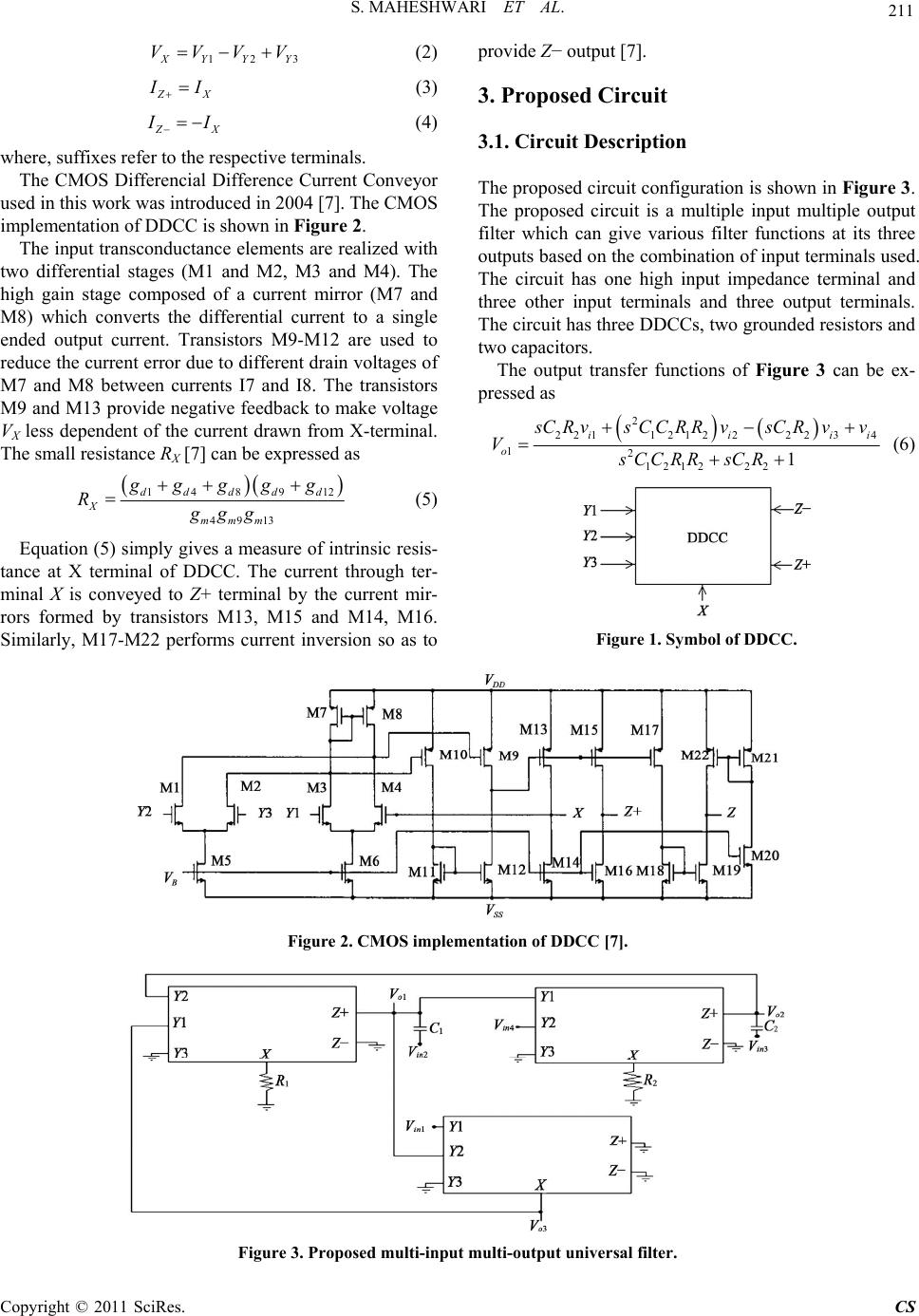 S. MAHESHWARI ET AL. 211 312XY YY VVVV (2) Z X I I (3) Z X I I (4) where, suffixes refer to the respective terminals. The CMOS Differencial Difference Current Conveyor used in this work was introduced in 2004 [7]. The CMOS implementation of DDCC is shown in Figure 2. The input transconductance elements are realized with two differential stages (M1 and M2, M3 and M4). The high gain stage composed of a current mirror (M7 and M8) which converts the differential current to a single ended output current. Transistors M9-M12 are used to reduce the current error due to different drain voltages of M7 and M8 between currents I7 and I8. The transistors M9 and M13 provide negative feedback to make voltage VX less dependent of the current drawn from X-terminal. The small resistance RX [7] can be expressed as 148912 4913 dd dd d X mmm gg gg g Rggg (5) Equation (5) simply gives a measure of intrinsic resis- tance at X terminal of DDCC. The current through ter- minal X is conveyed to Z+ terminal by the current mir- rors formed by transistors M13, M15 and M14, M16. Similarly, M17-M22 performs current inversion so as to provide Z− output [7]. 3. Proposed Circuit 3.1. Circuit Description The proposed circuit configuration is shown in Figure 3. The proposed circuit is a multiple input multiple output filter which can give various filter functions at its three outputs based on the combination of input terminals used. The circuit has one high input impedance terminal and three other input terminals and three output terminals. The circuit has three DDCCs, two grounded resistors and two capacitors. The output transfer functions of Figure 3 can be ex- pressed as 2 2211212 222 34 12 121222 1 ii o ii s CRvsCCRR vsCR vv VsCCRRsCR (6) Figure 1. Symbol of DDCC. Figure 2. CMOS implementation of DDCC [7]. Figure 3. Proposed multi-input multi-output universal filter. Copyright © 2011 SciRes. CS 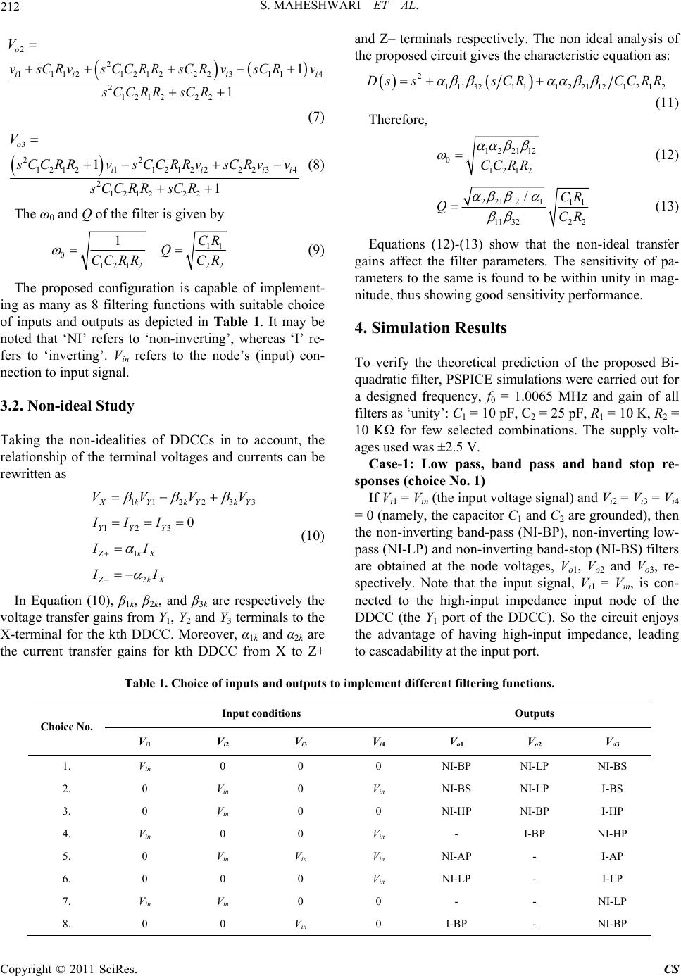 S. MAHESHWARI ET AL. Copyright © 2011 SciRes. CS 212 2 2 1112121222311 2 1212 22 1 1 o ii i V vsCR vsC CR RsCRvsCRv sCCRR sCR 4i (7) 3 22 1212112122223 4 2 1212 22 1 1 o iii V i s CC RRvs CCRRvsC Rvv sCCRR sCR (8) The ω0 and Q of the filter is given by 11 0 1212 22 1CR Q CC RRC R (9) The proposed configuration is capable of implement- ing as many as 8 filtering functions with suitable choice of inputs and outputs as depicted in Table 1. It may be noted that ‘NI’ refers to ‘non-inverting’, whereas ‘I’ re- fers to ‘inverting’. Vin refers to the node’s (input) con- nection to input signal. 3.2. Non-ideal Study Taking the non-idealities of DDCCs in to account, the relationship of the terminal voltages and currents can be rewritten as 112 23 3 123 1 2 0 XkY kYkY YY Y ZkX ZkX VVV V III II II (10) In Equation (10), β1k, β2k, and β3k are respectively the voltage transfer gains from Y1, Y2 and Y3 terminals to the X-terminal for the kth DDCC. Moreover, α1k and α2k are the current transfer gains for kth DDCC from X to Z+ and Z– terminals respectively. The non ideal analysis of the proposed circuit gives the characteristic equation as: 2 11132111 221121 2 1 2 Ds ssCRCCRR (11) Therefore, 1221 12 0 1212 CC RR (12) 22112 111 11 3222 /CR QCR (13) Equations (12)-(13) show that the non-ideal transfer gains affect the filter parameters. The sensitivity of pa- rameters to the same is found to be within unity in mag- nitude, thus showing good sensitivity performance. 4. Simulation Results To verify the theoretical prediction of the proposed Bi- quadratic filter, PSPICE simulations were carried out for a designed frequency, f0 = 1.0065 MHz and gain of all filters as ‘unity’: C1 = 10 pF, C2 = 25 pF, R1 = 10 K, R2 = 10 KΩ for few selected combinations. The supply volt- ages used was ±2.5 V. Case-1: Low pass, band pass and band stop re- sponses (choice No. 1) If Vi1 = Vin (the input voltage signal) and Vi2 = Vi3 = Vi4 = 0 (namely, the capacitor C1 and C2 are grounded), then the non-inverting band-pass (NI-BP), non-inverting low- pass (NI-LP) and non-inverting band-stop (NI-BS) filters are obtained at the node voltages, Vo1, Vo2 and Vo3, re- spectively. Note that the input signal, Vi1 = Vin, is con- nected to the high-input impedance input node of the DDCC (the Y1 port of the DDCC). So the circuit enjoys the advantage of having high-input impedance, leading to cascadability at the input port. Table 1. Choice of inputs and outputs to implement diffe re nt filter ing func tions. Input conditions Outputs Choice No. Vi1 Vi2 Vi3 Vi4 Vo1 Vo2 Vo3 1. Vin 0 0 0 NI-BP NI-LP NI-BS 2. 0 Vin 0 Vin NI-BS NI-LP I-BS 3. 0 Vin 0 0 NI-HP NI-BP I-HP 4. Vin 0 0 Vin - I-BP NI-HP 5. 0 Vin Vin Vin NI-AP - I-AP 6. 0 0 0 Vin NI-LP - I-LP 7. Vin V in 0 0 - - NI-LP 8. 0 0 Vin 0 I-BP - NI-BP  S. MAHESHWARI ET AL. Copyright © 2011 SciRes. CS 213 Figure 4 shows the filter response for low pass, band pass and band reject functions. The low pass band width found is 0.89615 MHz. Similarly for band pass function the central frequency is 1.042 MHz and the band width is 1.041 MHz. While for the band reject function the central fre- quency found is 1.0278 MHz. Figure 5 shows the transient response of band pass filter for a sinusoidal input of 1 MHz. Case 2 : Inverting, non-inverting HP and BP filter (choice No. 3) If Vi2 = Vin (the input voltage signal) and Vi1 = Vi3 = Vi4 = 0 then non-inverting high-pass (NI-HP) function is implemented at Vo1 and inverting high pass function is obtained at Vo3. It may be noted that band-pass is also obtained at Vo2. Figures 6 and 7 shows the frequency responses of non-inverting and inverting high pass function. The cut off frequency for the high pass function of the proposed filter circuit has been found to be 1.21 MHz. Figure 8 shows the transient responses of non-inverting and in- verting high pass functions respectively for a sinusoidal input of 10 MHz. Also the THD of non-inverting high pass function is found to be 2.3%. It may be noted that the band-pass response is not shown in this case, for brevity reasons, as it was already covered in case 1. Figure 4. Frequency Response for choice no. 1. Figure 5. Input and outputs of BP filter at 1 MHz. 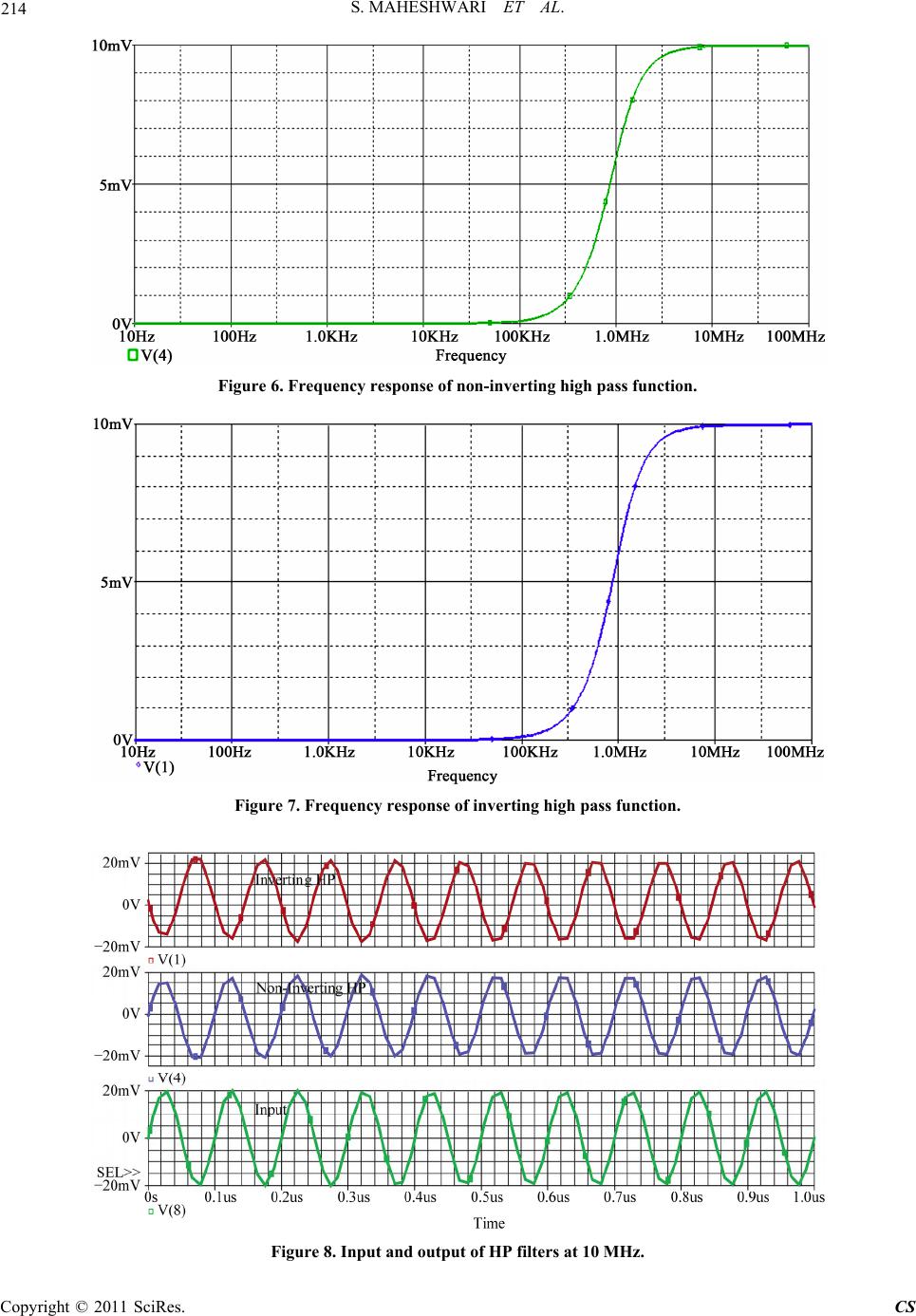 214 S. MAHESHWARI ET AL. Figure 6. Frequency response of non-inverting high pass function. Figure 7. Frequency response of inverting high pass function. Figure 8. Input and output of HP filters at 10 MHz. Copyright © 2011 SciRes. CS 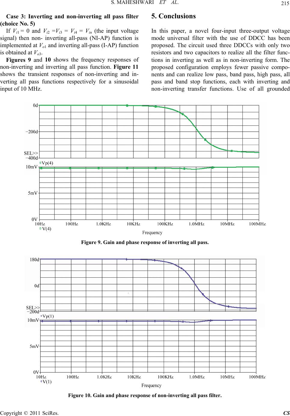 S. MAHESHWARI ET AL. Copyright © 2011 SciRes. CS 215 5. Conclusions Case 3: Inverting and non-inverting all pass filter (choice No. 5) If Vi1 = 0 and Vi2 =Vi3 = Vi4 = Vin (the input voltage signal) then non- inverting all-pass (NI-AP) function is implemented at Vo1 and inverting all-pass (I-AP) function is obtained at Vo3. In this paper, a novel four-input three-output voltage mode universal filter with the use of DDCC has been proposed. The circuit used three DDCCs with only two resistors and two capacitors to realize all the filter func- tions in inverting as well as in non-inverting form. The proposed configuration employs fewer passive compo- nents and can realize low pass, band pass, high pass, all pass and band stop functions, each with inverting and non-inverting transfer functions. Use of all grounded Figures 9 and 10 shows the frequency responses of non-inverting and inverting all pass function. Figure 11 shows the transient responses of non-inverting and in- verting all pass functions respectively for a sinusoidal input of 10 MHz. Figure 9. Gain and phase response of inverting all pass. Figure 10. Gain and phase response of non-inverting all pass filter. 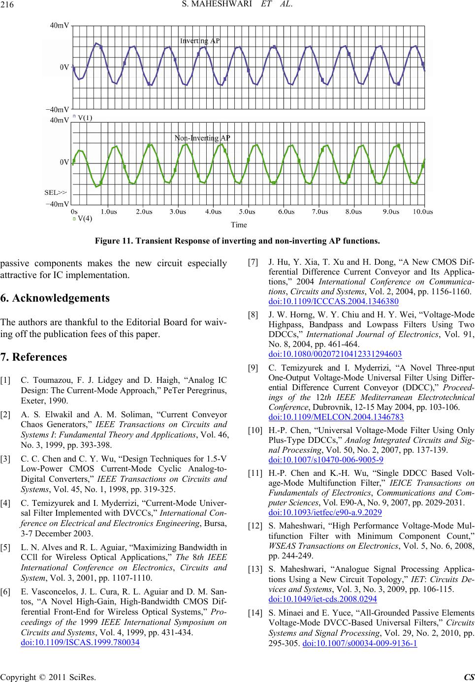 216 S. MAHESHWARI ET AL. Figure 11. Transient Response of inverting and non-inverting AP functions. passive components makes the new circuit especially attractive for IC implementation. 6. Acknowledgements The authors are thankful to the Editorial Board for waiv- ing off the publication fees of this paper. 7. References [1] C. Toumazou, F. J. Lidgey and D. Haigh, “Analog IC Design: The Current-Mode Approach,” PeTer Peregrinus, Exeter, 1990. [2] A. S. Elwakil and A. M. Soliman, “Current Conveyor Chaos Generators,” IEEE Transactions on Circuits and Systems I: Fundamental Theory and Applications, Vol. 46, No. 3, 1999, pp. 393-398. [3] C. C. Chen and C. Y. Wu, “Design Techniques for 1.5-V Low-Power CMOS Current-Mode Cyclic Analog-to- Digital Converters,” IEEE Transactions on Circuits and Systems, Vol. 45, No. 1, 1998, pp. 319-325. [4] C. Temizyurek and I. Myderrizi, “Current-Mode Univer- sal Filter Implemented with DVCCs,” International Con- ference on Electrical and Electronics Engineering, Bursa, 3-7 December 2003. [5] L. N. Alves and R. L. Aguiar, “Maximizing Bandwidth in CCll for Wireless Optical Applications,” The 8th IEEE International Conference on Electronics, Circuits and System, Vol. 3, 2001, pp. 1107-1110. [6] E. Vasconcelos, J. L. Cura, R. L. Aguiar and D. M. San- tos, “A Novel High-Gain, High-Bandwidth CMOS Dif- ferential Front-End for Wireless Optical Systems,” Pro- ceedings of the 1999 IEEE International Symposium on Circuits and Systems, Vol. 4, 1999, pp. 431-434. doi:10.1109/ISCAS.1999.780034 [7] J. Hu, Y. Xia, T. Xu and H. Dong, “A New CMOS Dif- ferential Difference Current Conveyor and Its Applica- tions,” 2004 International Conference on Communica- tions, Circuits and Systems, Vol. 2, 2004, pp. 1156-1160. doi:10.1109/ICCCAS.2004.1346380 [8] J. W. Horng, W. Y. Chiu and H. Y. Wei, “Voltage-Mode Highpass, Bandpass and Lowpass Filters Using Two DDCCs,” International Journal of Electronics, Vol. 91, o. 8, 2004, pp. 461-464. doi:10.1080/00207210412331294603 [9] C. Temizyurek and I. Myderrizi, “A Novel Three-nput One-Output Voltage-Mode Universal Filter Using Differ- ential Difference Current Conveyor (DDCC),” Proceed- ings of the 12th IEEE Mediterranean Electrotechnical Conference, Dubrovnik, 12-15 May 2004, pp. 103-106. doi:10.1109/MELCON.2004.1346783 [10] H.-P. Chen, “Universal Voltage-Mode Filter Using Only Plus-Type DDCCs,” Analog Integrated Circuits and Sig- nal Processing, Vol. 50, No. 2, 2007, pp. 137-139. doi:10.1007/s10470-006-9005-9 [11] H.-P. Chen and K.-H. Wu, “Single DDCC Based Volt- age-Mode Multifunction Filter,” IEICE Transactions on Fundamentals of Electronics, Communications and Com- puter Sciences, Vol. E90-A, No. 9, 2007, pp. 2029-2031. doi:10.1093/ietfec/e90-a.9.2029 [12] S. Maheshwari, “High Performance Voltage-Mode Mul- tifunction Filter with Minimum Component Count,” WSEAS Transactions on Electronics, Vol. 5, No. 6, 2008, pp. 244-249. [13] S. Maheshwari, “Analogue Signal Processing Applica- tions Using a New Circuit Topology,” IET: Circuits De- vices and Systems, Vol. 3, No. 3, 2009, pp. 106-115. doi:10.1049/iet-cds.2008.0294 [14] S. Minaei and E. Yuce, “All-Grounded Passive Elements Voltage-Mode DVCC-Based Universal Filters,” Circuits Systems and Signal Processing, Vol. 29, No. 2, 2010, pp. 295-305. doi:10.1007/s00034-009-9136-1 Copyright © 2011 SciRes. CS |