

Paper Menu >>
Journal Menu >>
 Circuits and Systems, 2011, 2, 190-195 doi:10.4236/cs.2011.23027 Published Online July 2011 (http://www.SciRP.org/journal/cs) Copyright © 2011 SciRes. CS Voltage Controlled Ring Oscillator Design with Novel 3 Transistors XNOR/XOR Gates Manoj Kumar1, Sandeep Kumar Arya1, Sujata Pandey2 1Department of Electronics & Communication Engineering Guru Jambheshwar, University of Science & Technology, Hisar , India 2Department of Electronics & Communication Engineering, Amity University, Noida, India E-mail: [email protected] Received April 14, 2011; revised May 6, 2011; accepted May 13, 2011 Abstract In present work, improved designs for voltage controlled ring oscillators (VCO) using three transistors XNOR/XOR gates have been presented. Supply voltage has been varied from [1.8 - 1.2] V in proposed de- signs. In first method, the VCO design using three XNOR delay cells shows frequency variation of [1.900 - 0.964] GHz with [279.429 - 16.515] µW power consumption variation. VCO designed with five XNOR de- lay cells shows frequency variation of [1.152 - 0.575] GHz with varying power consumption of [465.715 - 27.526] µW. In the second method VCO having three XOR stages shows frequency variation [1.9176 - 1.029] GHz with power consumption variation from [296.393 - 19.051] µW. A five stage XOR based VCO design shows frequency variation [1.049 - 0.565] GHz with power consumption variation from [493.989 - 31.753] µW. Simulations have been performed by using SPICE based on TSMC 0.18µm CMOS technology. Power con- sumption and output frequency range of proposed VCOs have been compared with earlier reported circuits and proposed circuit’s shows improved performance. Keywords: CMOS, Delay Cell, Low Power, VCO, XOR and XNOR Gates 1. Introduction The Phase locked loops (PLL) are widely used circuit component in data transmission systems and have exten- sive applications in data modulation, demodulation and mobile communication. Voltage control oscillators (VCO) are the critical and necessary building blocks of these PLL systems. Two widely used VCOs types are LC tank based and CMOS ring circuits. Combination of inductor and capacitor consumes large layout area in LC tank based oscillators [1-3]. CMOS ring based oscillators have advantages due to ease of controlling the output frequency and no requirement for on chip inductors [4,5]. CMOS based ring oscillators are easier to integrate and also gives wide tuning range. Due to flexibility of on chip integration, CMOS based ring oscillators have be- come essential building blocks in various battery oper- ated mobile communication systems. Rising requirement of portable devices like cellular phones, notebooks, per- sonal communication devices have aggressively en- hanced attention for power saving in these devices. Pow- er consumption in very large scale integration (VLSI) systems includes dynamic, static power and leakage power consumption. Dynamic power consumption re- sults from switching of load capacitance between two different voltages and dependent on frequency of opera- tion. Static power is contributed by direct path short cir- cuits currents between supply (Vdd) and ground (Vss) and it is dependent on leakage currents components [6,7]. VCOs being the major components in PLL system and is responsible for most of the power consumption. Some draw back of ring based oscillators includes large power consumption, phase noise and the limit of highest achievable frequency. In modern VCOs design power consumption and output frequency range are significant performance metrics [8-13]. A ring oscillator consist of delay stages, with output of last stage fed back to input of first stage. A VCO block diagram with single ended N-delay stages is shown in Figure 1. The ring must provide a phase shift of 2π and unity voltage gain for oscillation occurrence. Each delay cell also gives a phase shift of π/N, where N is number of delay stages. The remaining π phase shift is provided by dc inversion using the inverter delay cells. For single 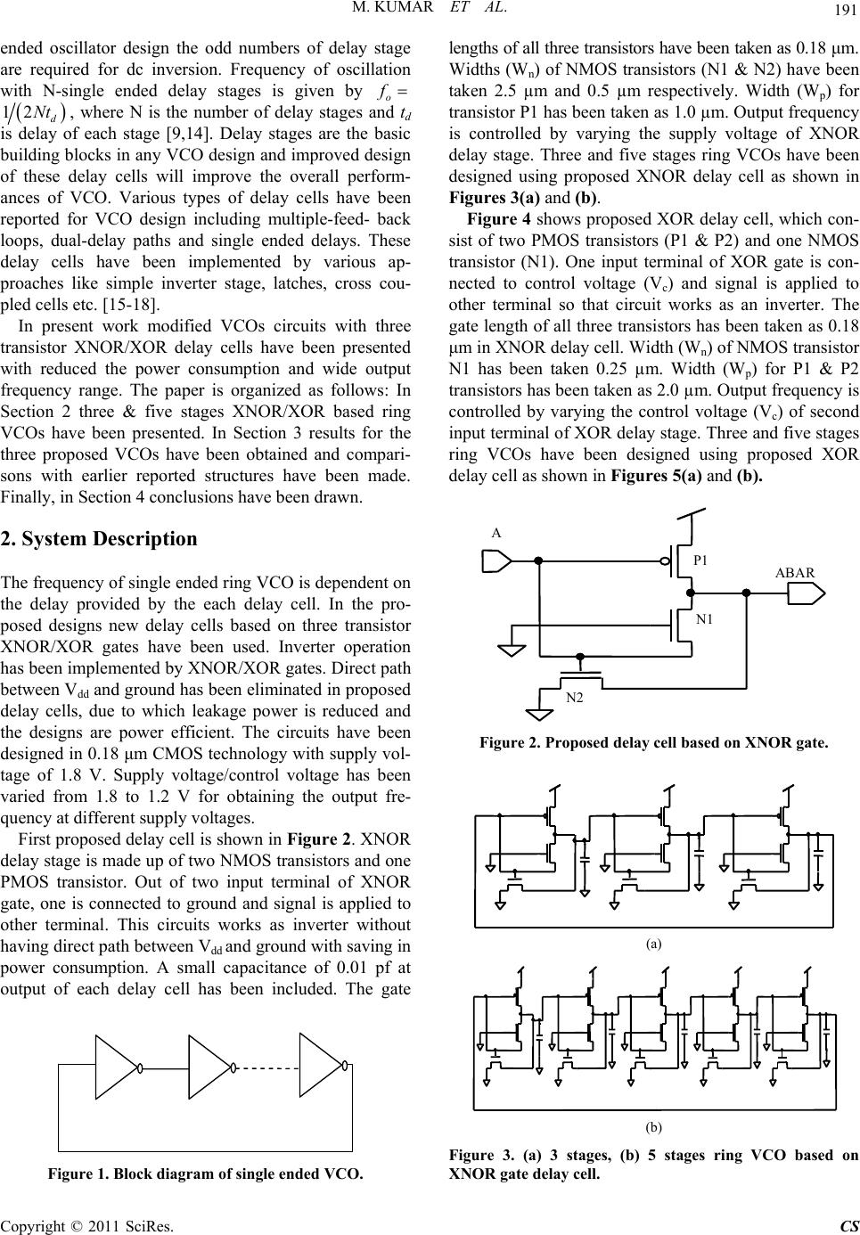 M. KUMAR ET AL. 191 ended oscillator design the odd numbers of delay stage are required for dc inversion. Frequency of oscillation with N-single ended delay stages is given by o f 12 d Nt , where N is the number of delay stages and td is delay of each stage [9,14]. Delay stages are the basic building blocks in any VCO design and improved design of these delay cells will improve the overall perform- ances of VCO. Various types of delay cells have been reported for VCO design including multiple-feed- back loops, dual-delay paths and single ended delays. These delay cells have been implemented by various ap- proaches like simple inverter stage, latches, cross cou- pled cells etc. [15-18]. In present work modified VCOs circuits with three transistor XNOR/XOR delay cells have been presented with reduced the power consumption and wide output frequency range. The paper is organized as follows: In Section 2 three & five stages XNOR/XOR based ring VCOs have been presented. In Section 3 results for the three proposed VCOs have been obtained and compari- sons with earlier reported structures have been made. Finally, in Section 4 conclusions have been drawn. 2. System Description The frequency of single ended ring VCO is dependent on the delay provided by the each delay cell. In the pro- posed designs new delay cells based on three transistor XNOR/XOR gates have been used. Inverter operation has been implemented by XNOR/XOR gates. Direct path between Vdd and ground has been eliminated in proposed delay cells, due to which leakage power is reduced and the designs are power efficient. The circuits have been designed in 0.18 μm CMOS technology with supply vol- tage of 1.8 V. Supply voltage/control voltage has been varied from 1.8 to 1.2 V for obtaining the output fre- quency at different supply voltages. First proposed delay cell is shown in Figure 2. XNOR delay stage is made up of two NMOS transistors and one PMOS transistor. Out of two input terminal of XNOR gate, one is connected to ground and signal is applied to other terminal. This circuits works as inverter without having direct path between Vdd and ground with saving in power consumption. A small capacitance of 0.01 pf at output of each delay cell has been included. The gate Figure 1. Block diagram of single ended VCO. lengths of all three transistors have been taken as 0.18 μm. Widths (Wn) of NMOS transistors (N1 & N2) have been taken 2.5 µm and 0.5 µm respectively. Width (Wp) for transistor P1 has been taken as 1.0 µm. Output frequency is controlled by varying the supply voltage of XNOR delay stage. Three and five stages ring VCOs have been designed using proposed XNOR delay cell as shown in Figures 3(a) and (b). Figure 4 shows proposed XOR delay cell, which con- sist of two PMOS transistors (P1 & P2) and one NMOS transistor (N1). One input terminal of XOR gate is con- nected to control voltage (Vc) and signal is applied to other terminal so that circuit works as an inverter. The gate length of all three transistors has been taken as 0.18 μm in XNOR delay cell. Width (Wn) of NMOS transistor N1 has been taken 0.25 µm. Width (Wp) for P1 & P2 transistors has been taken as 2.0 µm. Output frequency is controlled by varying the control voltage (Vc) of second input terminal of XOR delay stage. Three and five stages ring VCOs have been designed using proposed XOR delay cell as shown in Figures 5(a) and (b). A AB A R P1 N 1 N 2 Figure 2. Proposed delay cell based on XNOR gate. (a) (b) Figure 3. (a) 3 stages, (b) 5 stages ring VCO based on XNOR gate delay cell. Copyright © 2011 SciRes. CS 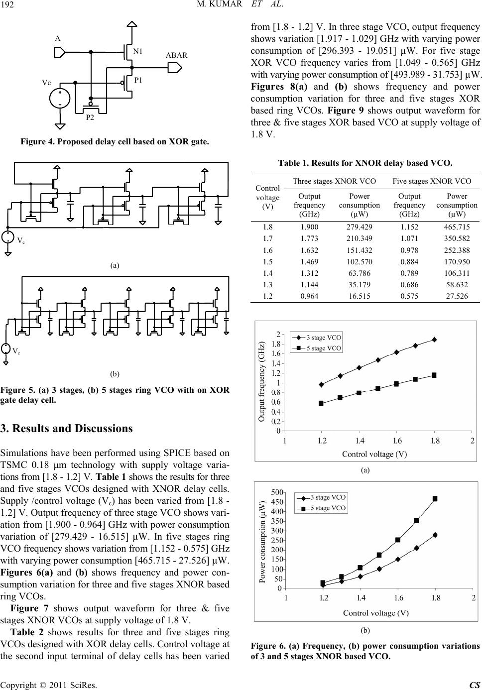 192 M. KUMAR ET AL. A ABA R V c N 1 P1 P2 Figure 4. Proposed delay cell based on XOR gate. V c (a) Vc ( Figure 5. (a) 3 stages, (b) 5 es ring VCO with on XOR . Results and Discussions imulations have been performed using SPICE based on ows output waveform for three & five st ges ring V Table 1. Results for XNOR delay based VCO. b) stag gate delay cell. 3 S TSMC 0.18 μm technology with supply voltage varia- tions from [1.8 - 1.2] V. Table 1 shows the results for three and five stages VCOs designed with XNOR delay cells. Supply /control voltage (Vc) has been varied from [1.8 - 1.2] V. Output frequency of three stage VCO shows vari- ation from [1.900 - 0.964] GHz with power consumption variation of [279.429 - 16.515] µW. In five stages ring VCO frequency shows variation from [1.152 - 0.575] GHz with varying power consumption [465.715 - 27.526] µW. Figures 6(a) and (b) shows frequency and power con- sumption variation for three and five stages XNOR based ring VCOs. Figure 7 sh ages XNOR VCOs at supply voltage of 1.8 V. Table 2 shows results for three and five sta COs designed with XOR delay cells. Control voltage at the second input terminal of delay cells has been varied from [1.8 - 1.2] V. In three stage VCO, output frequency shows variation [1.917 - 1.029] GHz with varying power consumption of [296.393 - 19.051] µW. For five stage XOR VCO frequency varies from [1.049 - 0.565] GHz with varying power consumption of [493.989 - 31.753] µW. Figures 8(a) and (b) shows frequency and power consumption variation for three and five stages XOR based ring VCOs. Figure 9 shows output waveform for three & five stages XOR based VCO at supply voltage of 1.8 V. Three stages XNOR VCO Five stages XNOR VCO Control fr con fr con voltage (V) Output Power equency (GHz) nsumptio (µW) Output Power equency (GHz) nsumptio (µW) 1.8 2 4 1.900 79.429 1.152 65.715 1.7 1.773 210.349 1.071 350.582 1.6 1.632 151.432 0.978 252.388 1.5 1.469 102.570 0.884 170.950 1.4 1.312 63.786 0.789 106.311 1.3 1.144 35.179 0.686 58.632 1.2 0.964 16.515 0.575 27.526 (a) (b) Figure 6. (a) Frequency, (b) power consumption variations of 3 and 5 stages XNOR based VCO. Copyright © 2011 SciRes. CS 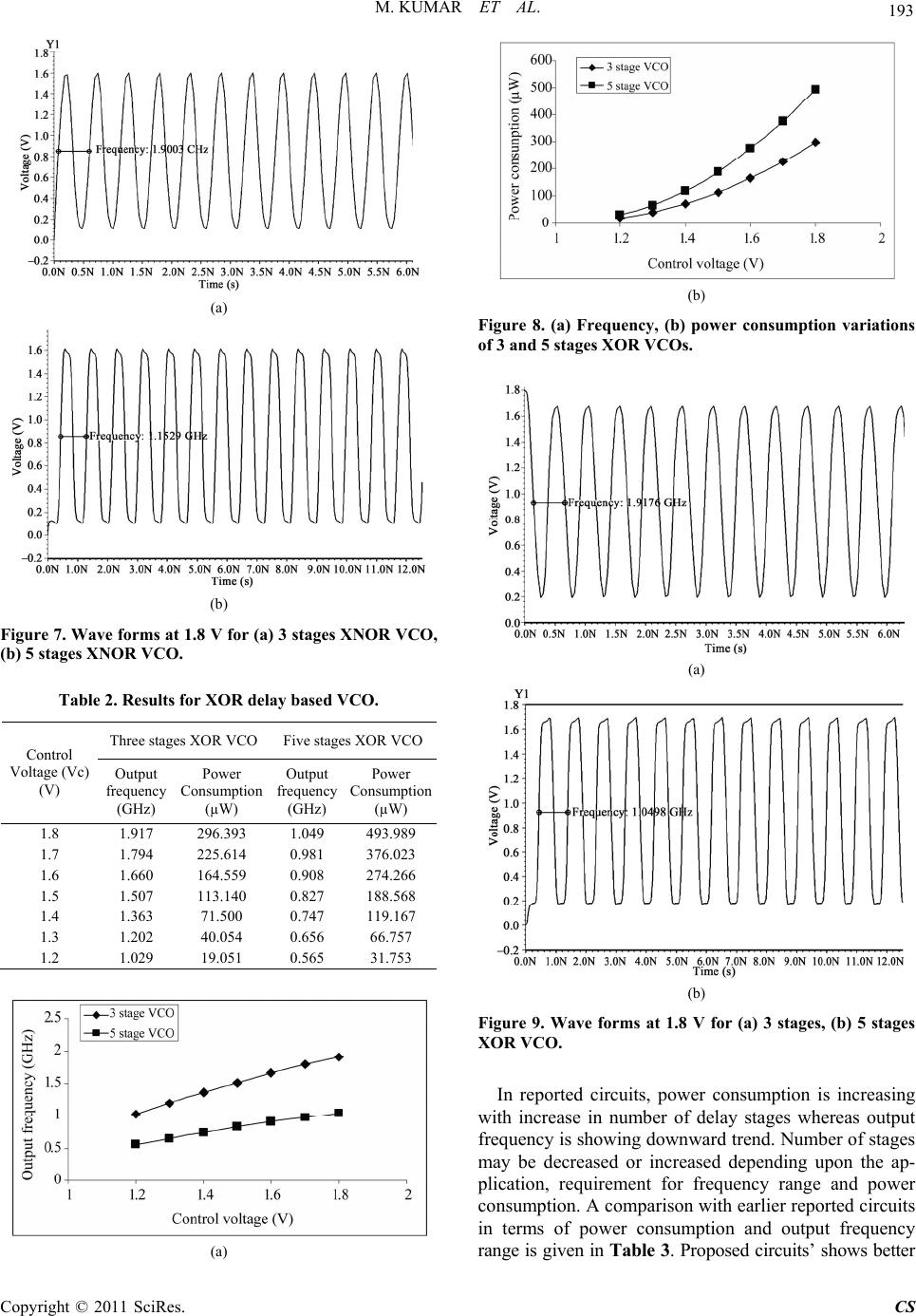 M. KUMAR ET AL. 193 (a) (b) Figure 7. Wave forms at 1.8r (a) 3 stages XNOR VCO, (b) 5 stages XNOR VCO. r XOR delay based VCO. VCO V fo Table 2. Results fo Three stages XOR VCO Five stages XOR Contr Voltage (Vc) fr fr ol (V) Output equency Power Consumption (GHz) (µW) Output equency Power Consumption (GHz) (µW) 1.8 1.917 296.393 1.049 493.989 1.7 2 3 1.794 25.6140.981 76.023 1.6 1.660 164.559 0.908 274.266 1.5 1.507 113.140 0.827 188.568 1.4 1.363 71.500 0.747 119.167 1.3 1.202 40.054 0.656 66.757 1.2 1.029 19.051 0.565 31.753 (b) Figure 8. (a) Frequency, (b) power consumption variations of 3 and 5 stages XOR VCOs. (a) (b) Figure 9. Wave forms at 1.8 V for (a) 3 stages, (b) 5 stages XOR VCO. In reported circuits, power consumption is increasing with increase in number of delay stages whereas output frequency is showing downward trend. Number of stages may be decreased or increased depending upon the ap- plication, requirement for frequency range and power consumption. A comparison with earlier reported circuits in terms of power consumption and output frequency range is given in Table 3. Proposed circuits’ shows better (a) Copyright © 2011 SciRes. CS 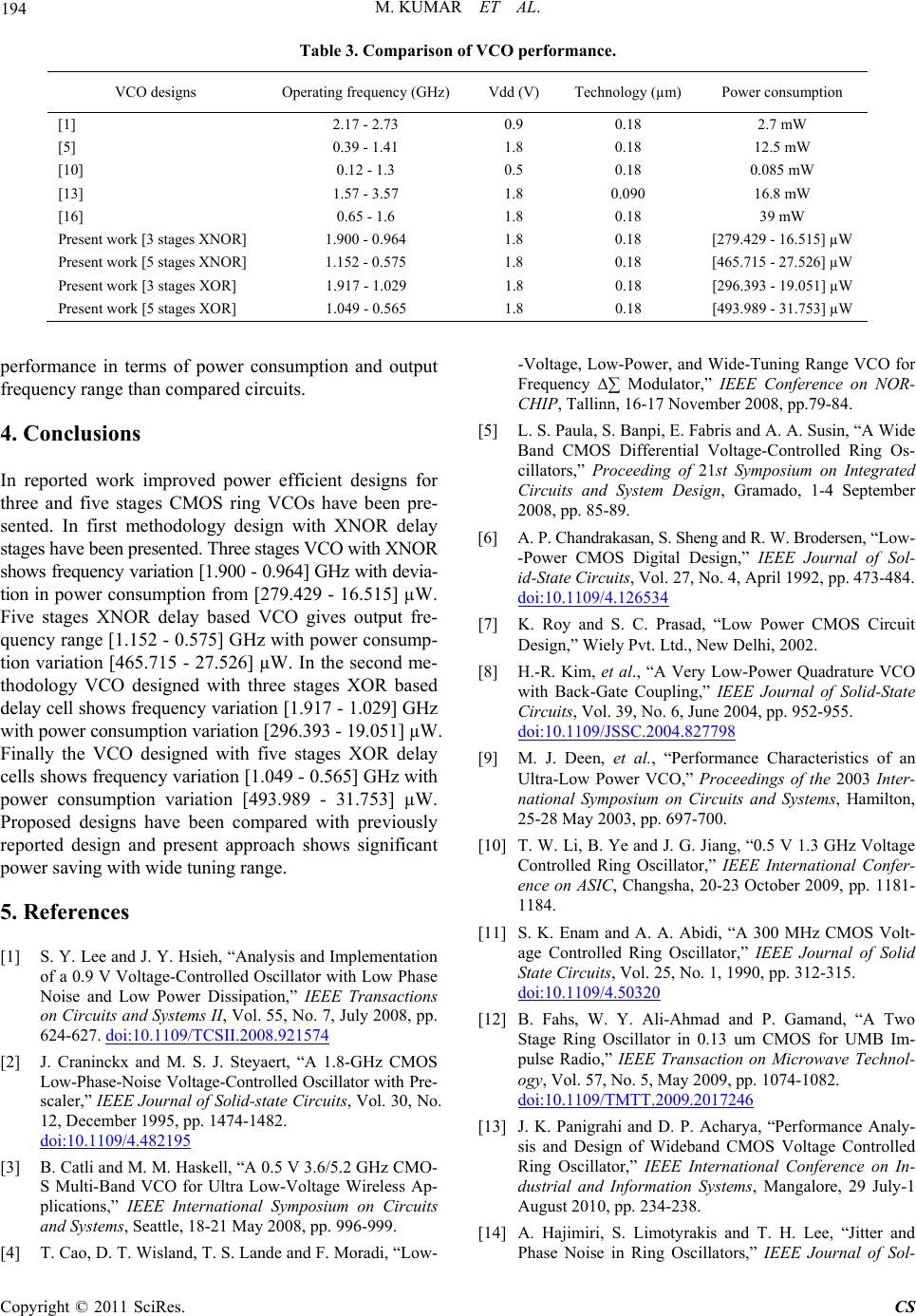 M. KUMAR ET AL. Copyright © 2011 SciRes. CS 194 Table 3. Comparison of VCO performance. Vdd (V) Technology (µm) Power consumption VCO designs Operating frequency (GHz) [1] 2.17 - 2.73 0.9 0.18 2.7 mW [5] 0.39 - 1.41 1.8 0.18 12.5 mW [10] 0.12 - 1.3 0.5 0.18 0.085 mW [13] 16.8 mW [16] 0.65 - 1.6 1.8 0.18 39 mW Present work [3 stages XNOR] [ ent work [5 stages XNOR] 1 [465.7 ent work [3 stages XOR] [296.3 µW nt work [5 stages XOR] 1. [493. µW 1.57 - 3.57 1.8 0.090 1.900 - 0.964 1.8 0.18 279.429 - 16.515] µW Pres.152 - 0.575 1.8 0.18 15 - 27.526] µW Pres1.917 - 1.029 1.8 0.18 93 - 19.051] Prese049 - 0.5651.8 0.18 989 - 31.753] perform in terms of power consumptiotput frequenircuits. 4. Con reported work improved power efficient designs for CO with XNOR iation [1.900 - 0.964] GHz with devia- ption from [279.429 - 16.515] µW. o. 7, July 2008, pp. 8.921574 ancen and ou cy range than compared c clusions In three and five stages CMOS ring VCOs have been pre- sented. In first methodology design with XNOR delay ages have been presented. Three stages Vst shows frequency var on in power consumti Five stages XNOR delay based VCO gives output fre- quency range [1.152 - 0.575] GHz with power consump- tion variation [465.715 - 27.526] µW. In the second me- thodology VCO designed with three stages XOR based delay cell shows frequency variation [1.917 - 1.029] GHz with power consumption variation [296.393 - 19.051] µW. Finally the VCO designed with five stages XOR delay cells shows frequency variation [1.049 - 0.565] GHz with power consumption variation [493.989 - 31.753] µW. Proposed designs have been compared with previously reported design and present approach shows significant power saving with wide tuning range. 5. References [1] S. Y. Lee and J. Y. Hsieh, “Analysis and Implementation of a 0.9 V Voltage-Controlled Oscillator with Low Phase Noise and Low Power Dissipation,” IEEE Transactions on Circuits and Systems II, Vol. 55, N 624-627. doi:10.1109/TCSII.200 nd M. S. J. Steyaert, “A 1.8-GHz CM Low-Phase-Noise Voltage-Controlled Oscillator with Pre- [2] J. Craninckx aOS scaler,” IEEE Journal of Solid-state Circuits, Vol. 30, No. 12, December 1995, pp. 1474-1482. doi:10.1109/4.482195 [3] B. Catli and M. M. Haskell, “A 0.5 V 3.6/5.2 GHz CMO- S Multi-Band VCO for Ultra Low-Voltage Wireless Ap- oltage, Lower, and Wide-Tange VCO for equency ∆∑ dulator,” n NOR- IP, Tallinn7 Nove [5] S. Paula, Si, E. Fa nd CMOSrential ing Os- cillators,” Proceeding of 21st Symposium on Integrated September plications,” IEEE International Symposium on Circuits and Systems, Seattle, 18-21 May 2008, pp. 996-999. [4] T. Cao, D. T. Wisland, T. S. Lande and F. Moradi, “Low- Circuits and System Design, Gramado, 1-4 2008, pp. 85-89. -V-Powuning R Fr Mo IEEE Conference o CH , 16-1mber 2008, pp.79-84. L.. Banpbris and A. A. Susin, “A Wide Ba DiffeVoltage-Controlled R [6] A. P. Chandrakasan, S. Sheng and R. W. Brodersen, “Low- -Power CMOS Digital Design,” IEEE Journal of Sol- id-State Circuits, Vol. 27, No. 4, April 1992, pp. 473-484. doi:10.1109/4.126534 [7] K. Roy and S. C. Prasad, “Low Power CMOS Circuit Design,” Wiely Pvt. Ltd., New Delhi, 2002. [8] H.-R. Kim, et al., “A Very Low-Power Quadrature VCO with Back-Gate Coupling,” IEEE Journal of Solid-State Circuits, Vol. 39, No. 6, June 2004, pp. 952-955. doi:10.1109/JSSC.2004.827798 [9] M. J. Deen, et al., “Performance Characteristics of an Ultra-Low Power VCO,” Proceedings of the 2003 Inter- national Symposium on Circuits and Systems, Hamilton, 25-28 May 2003, pp. 697-700. [10] T. W. Li, B. Ye and J. G. Jiang, “0.5 V 1.3 GHz Voltage Controlled Ring Oscillator,” IEEE International Confer- ence on ASIC, Changsha, 20-23 October 2009, pp. 1181- 1184. [11] S. K. Enam and A. A. Abidi, “A 300 MHz CMOS Volt- age Controlled Ring Oscillator,” IEEE Journal of Solid State Circuits, Vol. 25, No. 1, 1990, pp. 312-315. doi:10.1109/4.50320 [12] B. Fahs, W. Y. Ali-Ahmad and P. Gamand, “A Two Stage Ring Oscillator in 0.13 um CMOS for UMB Im- pulse Radio,” IEEE Transaction on Microwave Technol- ogy, Vol. 57, No. 5, May 2009, pp. 1074-1082. doi:10.1109/TMTT.2009.2017246 [13] J. K. Panigrahi and D. P. Acharya, “Performance Analy- sis and Design of Wideband CMOS Voltage Controlled Ring Oscillator,” IEEE International Conference on In- dustrial and Information Systems, Mangalore, 29 July-1 August 2010, pp. 234-238. [14] A. Hajimiri, S. Limotyrakis and T. H. Lee, “Jitter and Phase Noise in Ring Oscillators,” IEEE Journal of Sol-  M. KUMAR ET AL. 195 id-State Circuits, Vol. 34, No. 6, June 1999, pp. 790-804. doi:10.1109/4.766813 -NoiseWide-Frequen- of Solid-State Circuits, SC.2003.820869 [15] H. Q. Liu, W. L. Goh and L. Siek, “A 0.18-µm 10-GHz CMOS Ring Oscillator for Optical Transceivers,” IEEE International Symposium on Circuits and Systems, Kobe, 23-26 May 2005, pp. 1525-1528. [16] S. L. Amakawa, et al., “Low-Phase cy-Range Ring-VCO-Based Scalable PLL with Sub Harmonic Injection Locking in 0.18 µM CMOS,” IEEE International Microwave Symposium Digest, Anaheim, 23-28 May 2010, pp. 1178-1181. [17] C. H. Park and B. Kim, “A Low-Noise, 900-Mhz VCO in 0.6-µm CMOS,” IEEE Journal Vol. 34, No. 5, May 1999, pp. 586-591. [18] Y. A. Eken and J. P. Uyemura, “A 5.9-GHz Voltage Controlled Ring Oscillator in 0.18-um CMOS,” IEEE Journal of Solid State Circuits, Vol. 39, No. 1, January 2004, pp. 230-233. doi:10.1109/JS Copyright © 2011 SciRes. CS |