

Paper Menu >>
Journal Menu >>
 Circuits and Systems, 2011, 2, 162-169 doi:10.4236/cs.2011.23024 Published Online July 2011 (http://www.SciRP.org/journal/cs) Copyright © 2011 SciRes. CS A Review of PVT Compensation Circuits for Advanced CMOS Technologies Andrey Malkov, Dmitry Vasiounin, Oleg Semenov Freescale Semicond ucto r, Moscow, Russia E-mail: [email protected] Received January 30, 2010; revised April 18, 2011; accepted April 25, 2011 Abstract The recent high-performance interfaces like DDR2, DDR3, USB and Serial ATA require their output drivers to provide a minimum variation of rise and fall times over Process, Voltage, and Temperature (PVT) and output load variations. As the interface speed grows up, the output drivers have been important component for high quality signal integrity, because the output voltage levels and slew rate are mainly determined by the output drivers. The output driver impedance compliance with the transmission line is a key factor in noise minimization due to the signal reflections. In this paper, the different implementations of PVT compensation circuits are analyzed for cmos45 nm and cmos65 nm technology processes. One of the considered PVT com- pensation circuits uses the analog compensation approach. This circuit was designed in cmos45 nm technol- ogy. Other two PVT compensation circuits use the digital compensation method. These circuits were de- signed in cmos65 nm technology. Their electrical characteristics are matched with the requirements for I/O drivers with respect to DDR2 and DDR3 standards. DDR2 I/O design was done by the Freescale wireless design team for mobile phones and later was re-used for other high speed interface designs. In conclusion, the advantages and disadvantages of considered PVT control circuits are analyzed. Keywords: PVT Compensation, PVT Control Circuit, Process Variation, DDR Interface, I/O Driver 1. Introduction In any manufacturing step during the fabrication process of ICs, there are target specifications and there are man- ufacturing tolerances around each specification. For ex- ample, the gate oxide thickness specification translates to slower devices (higher threshold voltage) for thicker ox- ides and faster devices for thinner oxides (lower thresh- old voltage). If such devices were used as a driver ele- ment, large variations in driver strengths and slew rates from the pre-driver should be expected. This is turn af- fects the timing of the outgoing signals. Providing the higher data processing rate and interface speed are becoming more important to the evolution of multimedia environment. For example, the speed of modern storage interfaces (ATA/ATAPI-6 standard) has rapidly increased up to 100 MB/s [1]. The recent high- performance interfaces like DDR2, DDR3, USB and Serial ATA require their output drivers to provide a minimum variation of rise and fall times over process, voltage, and temperature (PVT) and output load varia- tions. As the interface speed grows up, the output drivers have been important component for high quality signal integrity, because the output voltage levels and slew rate are mainly determined by the output drivers. Any de- crease in the skews variation depending on the PVT variations can usually be translated into better timing budgets and signal integrity, resulting in the increase of system I/O speed. To achieve good signal integrity, slew rate also must be kept constant over PVT variations. Large slew rate induces significant switching noise (Ldi/dt noise) and small slew rate decrease the signal timing margin. One method to improve system speed is to provide circuit compensation. The compensation al- lows the designer to speed up the slower I/O driver and receiver speeds and increase the driver strength for the slow part. At the same time, the fast part is slowed down to match the slow part in speed and drive strength. Vari- ous compensation architectures have been previously reported for PVT variation [2-5] and most of them use external resistors to generate a bias current. Generally, the PVT control circuits can be classified on two types with (1) analog and (2) digital compensation methods, as it shown in Figure 1. In this paper, the different imple- 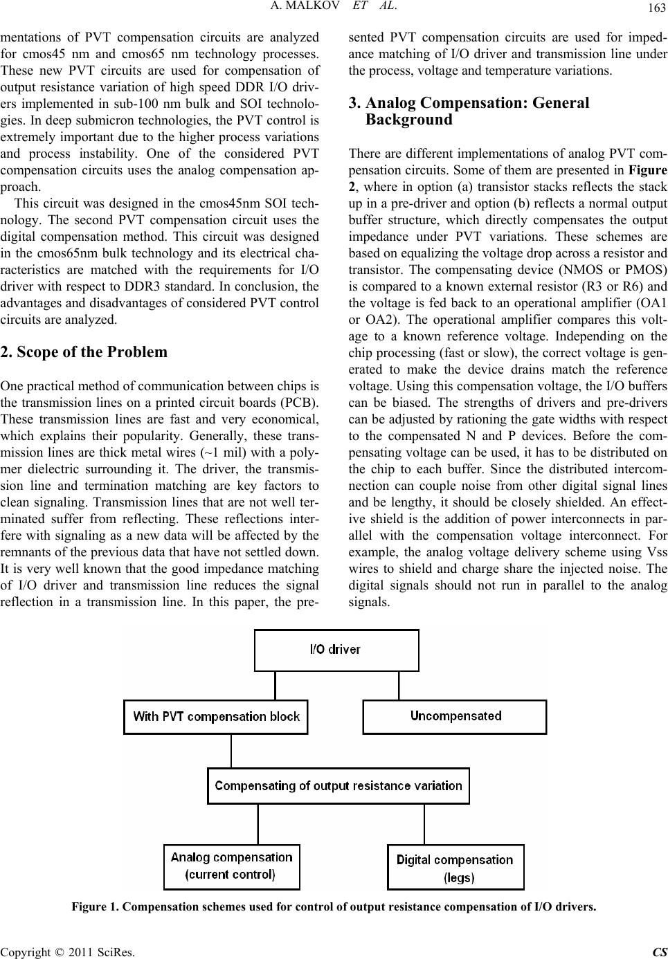 A. MALKOV ET AL. 163 mentations of PVT compensation circuits are analyzed for cmos45 nm and cmos65 nm technology processes. These new PVT circuits are used for compensation of output resistance variation of high speed DDR I/O driv- ers implemented in sub-100 nm bulk and SOI technolo- gies. In deep submicron technologies, the PVT control is extremely important due to the higher process variations and process instability. One of the considered PVT compensation circuits uses the analog compensation ap- proach. This circuit was designed in the cmos45nm SOI tech- nology. The second PVT compensation circuit uses the digital compensation method. This circuit was designed in the cmos65nm bulk technology and its electrical cha- racteristics are matched with the requirements for I/O driver with respect to DDR3 standard. In conclusion, the advantages and disadvantages of considered PVT control circuits are analyzed. 2. Scope of the Problem One practical method of communication between chips is the transmission lines on a printed circuit boards (PCB). These transmission lines are fast and very economical, which explains their popularity. Generally, these trans- mission lines are thick metal wires (~1 mil) with a poly- mer dielectric surrounding it. The driver, the transmis- sion line and termination matching are key factors to clean signaling. Transmission lines that are not well ter- minated suffer from reflecting. These reflections inter- fere with signaling as a new data will be affected by the remnants of the previous data that h ave not settled do wn. It is very well known that the good impedance matching of I/O driver and transmission line reduces the signal reflection in a transmission line. In this paper, the pre- sented PVT compensation circuits are used for imped- ance matching of I/O driver and transmission line under the process, voltage and temperature variations. 3. Analog Compensation: General Background There are different implementations of analog PVT com- pensation circuits. Some of them are presented in Figure 2, where in option (a) transistor stacks reflects the stack up in a pre-driver and option (b) reflects a normal output buffer structure, which directly compensates the output impedance under PVT variations. These schemes are based on equalizing the voltage drop across a resistor and transistor. The compensating device (NMOS or PMOS) is compared to a known external resistor (R3 or R6) and the voltage is fed back to an operational amplifier (OA1 or OA2). The operational amplifier compares this volt- age to a known reference voltage. Independing on the chip processing (fast or slow), the correct voltag e is gen- erated to make the device drains match the reference voltage. Using this compensation voltage, the I/O buffers can be biased. The strengths of drivers and pre-drivers can be adjusted by rationing the gate widths with respect to the compensated N and P devices. Before the com- pensating voltage can be used, it has to be distributed on the chip to each buffer. Since the distributed intercom- nection can couple noise from other digital signal lines and be lengthy, it should be closely shielded. An effect- ive shield is the addition of power interconnects in par- allel with the compensation voltage interconnect. For example, the analog voltage delivery scheme using Vss wires to shield and charge share the injected noise. The digital signals should not run in parallel to the analog signals. Figure 1. Compensation schemes used for control of output resistance compensation of I/O drivers. Copyright © 2011 SciRes. CS 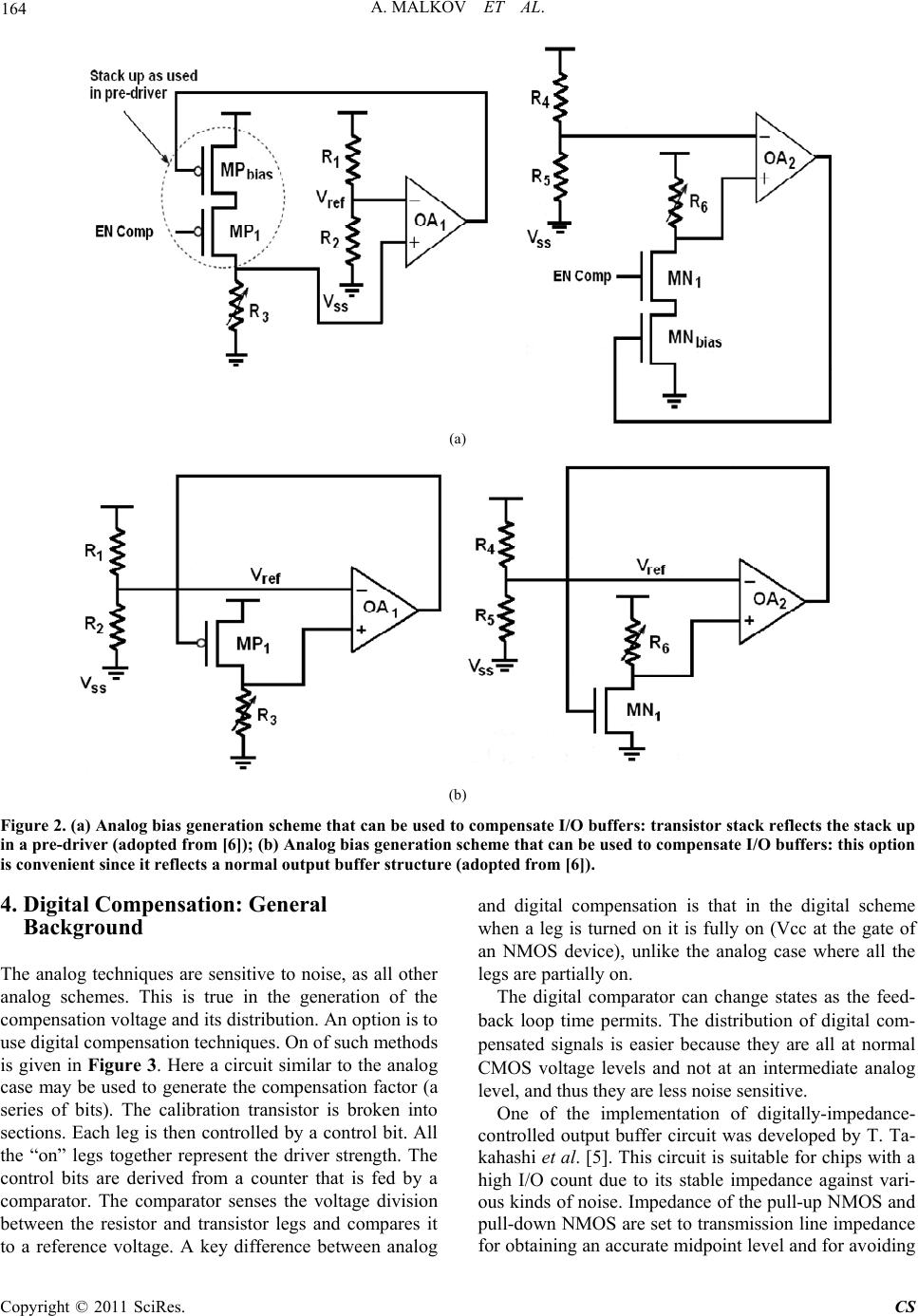 164 A. MALKOV ET AL. (a) (b) Figure 2. (a) Analog bias generation scheme that can be used to compensate I/O buffers: transistor stack reflects the stack up in a pre-driver (adopted from [6]); (b) Analog bias generation scheme that can be used to compensate I/O buffers: this option is convenient since it reflects a normal output buffer structure (adopted from [6]). 4. Digital Compensation: General Background The analog techniques are sensitive to noise, as all other analog schemes. This is true in the generation of the compensation voltage and its d istributio n. An option is to use digital compensation techniques. On of such methods is given in Figure 3. Here a circuit similar to the analog case may be used to generate the compensation factor (a series of bits). The calibration transistor is broken into sections. Each leg is then controlled by a control bit. All the “on” legs together represent the driver strength. The control bits are derived from a counter that is fed by a comparator. The comparator senses the voltage division between the resistor and transistor legs and compares it to a reference voltage. A key difference between analog and digital compensation is that in the digital scheme when a leg is turned on it is fully on (Vcc at the gate of an NMOS device), unlike the analog case where all the legs are partially on. The digital comparator can change states as the feed- back loop time permits. The distribution of digital com- pensated signals is easier because they are all at normal CMOS voltage levels and not at an intermediate analog level, and thus they are less noise sensitiv e. One of the implementation of digitally-impedance- controlled output buffer circuit was developed by T. Ta- kahashi et al. [5]. Th is circuit is suitable for chips with a high I/O count due to its stable impedance against vari- ous kinds of noise. Impedance of the pull-up NMOS and pull-down NMOS are set to transmission line impedance for obtaining an accurate midpoint level and for avoiding Copyright © 2011 SciRes. CS 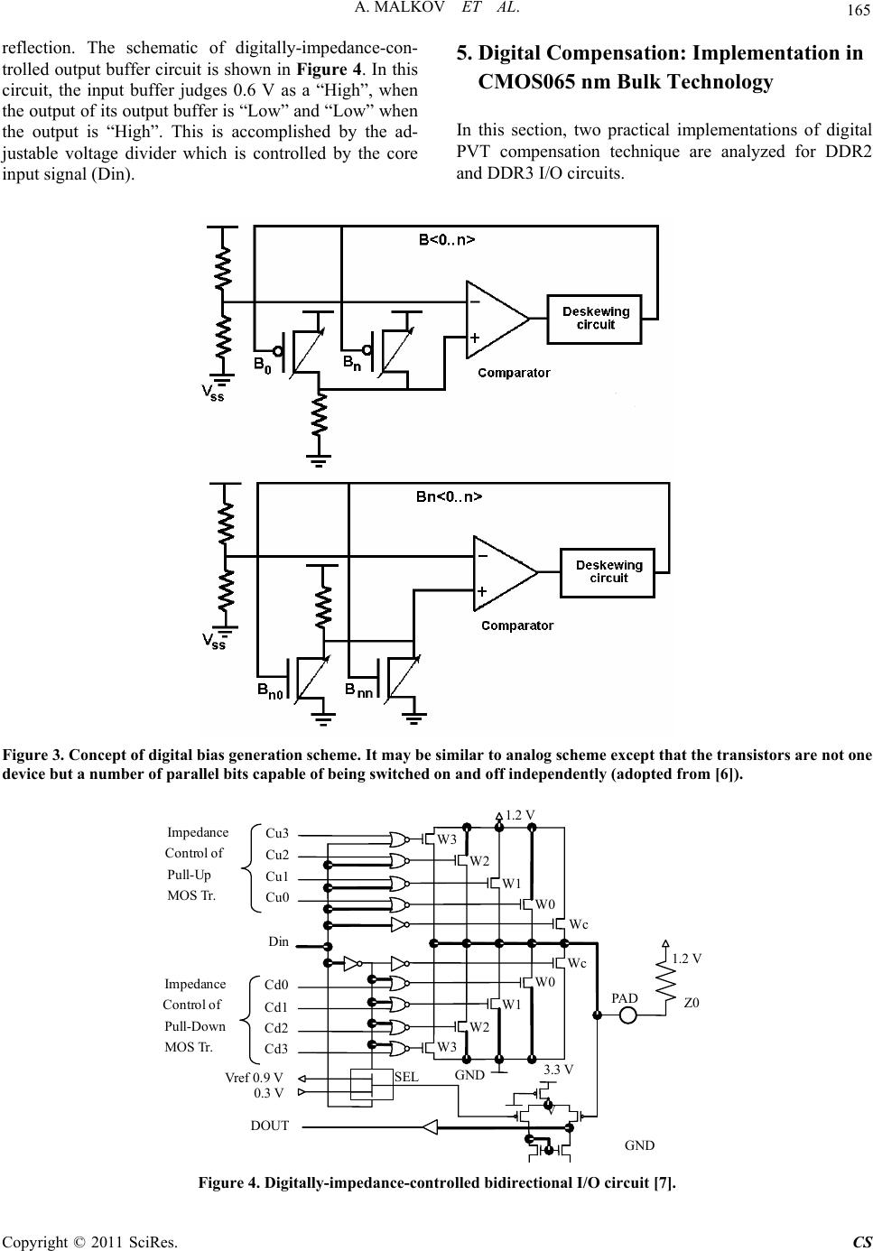 A. MALKOV ET AL. 165 reflection. The schematic of digitally-impedance-con- trolled output buffer circuit is shown in Figure 4. In th is circuit, the input buffer judges 0.6 V as a “High”, when the output of its output buffer is “Low” and “Low” when the output is “High”. This is accomplished by the ad- justable voltage divider which is controlled by the core input signal (Din). 5. Digital Compensation: Implementation in CMOS065 nm Bulk Technology In this section, two practical implementations of digital PVT compensation technique are analyzed for DDR2 and DDR3 I/O circuits. Figure 3. Concept of digital bias generation scheme. It may be similar to analog scheme except that the transistors are not one device but a number of parallel bits capable of be ing switche d on and off inde pendently (adopted from [6]). Cu3 Cu2 Cu1 Cu0 Impedance Control o f Pull-Down MOS Tr. Impedance Control of Pull-Up MOS Tr. Cd0 Cd1 Cd2 Cd3 Din Vref 0.9 V 0.3 V DOUT GND SEL PAD 3.3 V V W3 W2 W1 W0 Wc Wc W0 W1 W2 W3 GND 1.2 V Z0 1.2 V Figure 4. Digitally-impedance -control led bidirectional I/O circuit [7]. Copyright © 2011 SciRes. CS 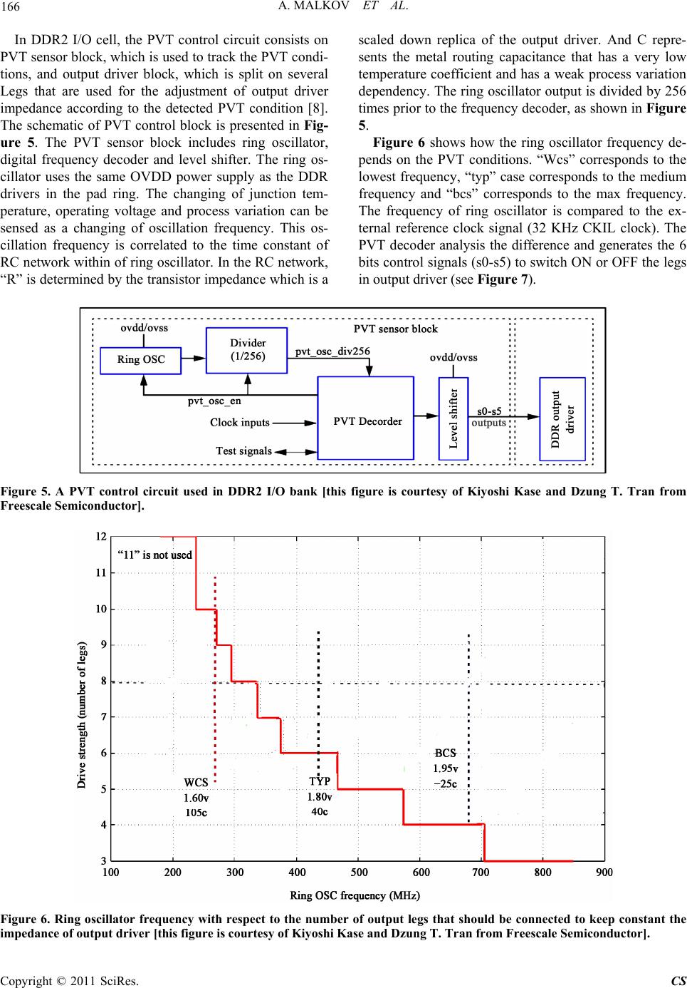 A. MALKOV ET AL. Copyright © 2011 SciRes. CS 166 In DDR2 I/O cell, the PVT control circuit consists on PVT sensor block, which is used to tr ack the PVT condi- tions, and output driver block, which is split on several Legs that are used for the adjustment of output driver impedance according to the detected PVT condition [8]. The schematic of PVT control block is presented in Fig- ure 5. The PVT sensor block includes ring oscillator, digital frequency decoder and level shifter. The ring os- cillator uses the same OVDD power supply as the DDR drivers in the pad ring. The changing of junction tem- perature, operating voltage and process variation can be sensed as a changing of oscillation frequency. This os- cillation frequency is correlated to the time constant of RC network within of ring oscillator. In the RC network, “R” is determined by the transistor impedance which is a scaled down replica of the output driver. And C repre- sents the metal routing capacitance that has a very low temperature coefficient and has a weak process variation dependency. The ring oscillator output is divided b y 256 times prior to the frequency decoder, as shown in Figure 5. Figure 6 shows how the ring oscillator frequency de- pends on the PVT conditions. “Wcs” corresponds to the lowest frequency, “typ” case corresponds to the medium frequency and “bcs” corresponds to the max frequency. The frequency of ring oscillator is compared to the ex- ternal reference clock signal (32 KHz CKIL clock). The PVT decoder analysis the difference and generates the 6 bits control signals (s0-s5) to switch ON or OFF the legs in output driver (see Figure 7). Figure 5. A PVT control circuit used in DDR2 I/O bank [this figure is courtesy of Kiyoshi Kase and Dzung T. Tran from Freescale Semiconduc tor]. Figure 6. Ring oscillator frequency with respect to the number of output legs that should be connected to keep constant the mpedance of output driver [this figure is courtesy of Kiyoshi Kase and Dzung T. Tran from Free sc ale Semiconductor]. i 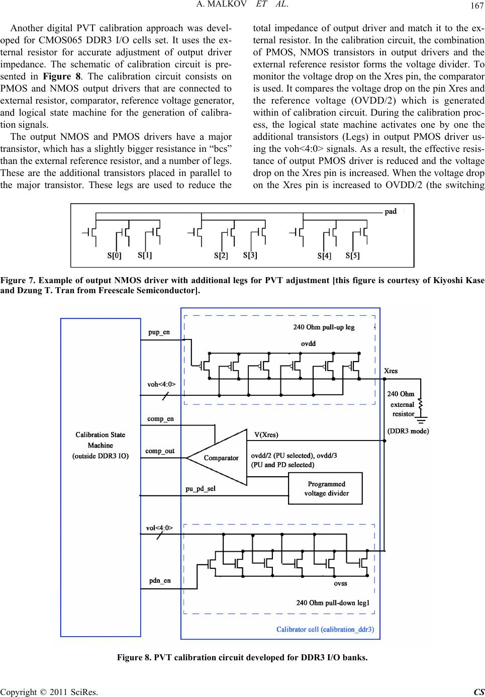 A. MALKOV ET AL. 167 Another digital PVT calibration approach was devel- oped for CMOS065 DDR3 I/O cells set. It uses the ex- ternal resistor for accurate adjustment of output driver impedance. The schematic of calibration circuit is pre- sented in Figure 8. The calibration circuit consists on PMOS and NMOS output drivers that are connected to external resistor, comparator, reference voltage generator, and logical state machine for the generation of calibra- tion signals. The output NMOS and PMOS drivers have a major transistor, which has a slightly bigger resistance in “bcs” than the external reference resistor, and a number of legs. These are the additional transistors placed in parallel to the major transistor. These legs are used to reduce the total impedance of output driver and match it to the ex- ternal resistor. In the calibration circuit, the combination of PMOS, NMOS transistors in output drivers and the external reference resistor forms the voltage divider. To monitor the voltag e drop on the Xres pin, the comparator is used. It compares the voltage drop on the pin Xres and the reference voltage (OVDD/2) which is generated within of calibration circuit. During the calibration proc- ess, the logical state machine activates one by one the additional transistors (Legs) in output PMOS driver us- ing the voh<4:0> signals. As a result, the effective resis- tance of output PMOS driver is reduced and the voltage drop on the Xres pin is increased. When the voltage drop on the Xres pin is increased to OVDD/2 (the switching Figure 7. Example of output NMOS driver with additional legs for PVT adjustment [this figure is courtesy of Kiyoshi Kase and Dzung T. Tran from Freescale Se mic onduc tor]. Figure 8. PVT calibration circuit developed for DDR3 I/O banks. Copyright © 2011 SciRes. CS 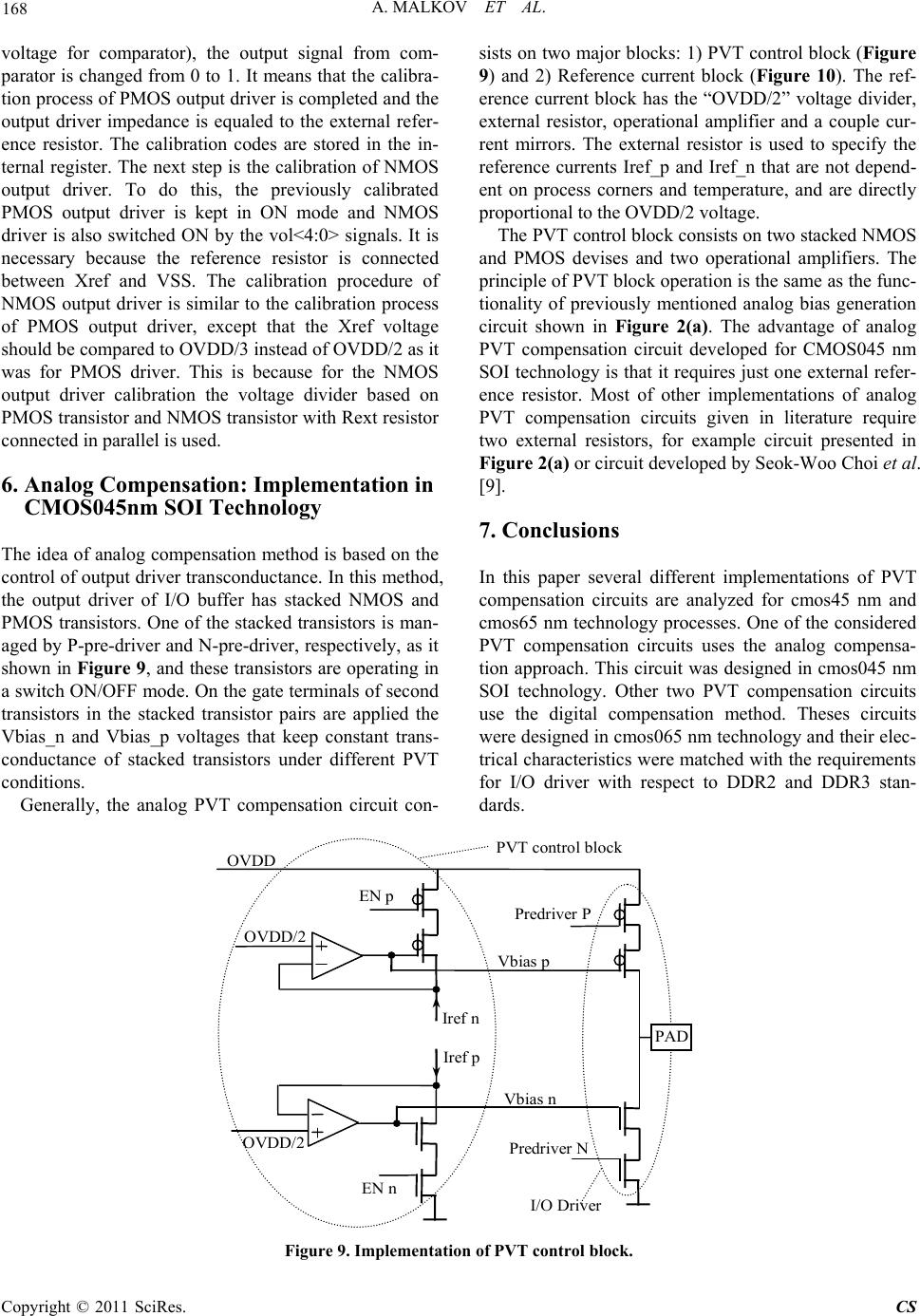 A. MALKOV ET AL. Copyright © 2011 SciRes. CS 168 voltage for comparator), the output signal from com- parator is changed from 0 to 1. It means that the calibra- tion process of PMOS output driver is completed and the output driver impedance is equaled to the external refer- ence resistor. The calibration codes are stored in the in- ternal register. The next step is the calibration of NMOS output driver. To do this, the previously calibrated PMOS output driver is kept in ON mode and NMOS driver is also switched ON by the vol<4:0> signals. It is necessary because the reference resistor is connected between Xref and VSS. The calibration procedure of NMOS output driver is similar to the calibration process of PMOS output driver, except that the Xref voltage should b e co mp ar ed to OV DD /3 instead of OVDD/2 as it was for PMOS driver. This is because for the NMOS output driver calibration the voltage divider based on PMOS transistor and NMOS transistor with Rext resistor connected in parallel is used. 6. Analog Compensation: Implementation in CMOS045nm SOI Technology The idea of analog compensation method is based on the control of output driver transconductance. In this method, the output driver of I/O buffer has stacked NMOS and PMOS transistors. One of the stacked transistors is man- aged by P-pre-driver and N-pre-driver, respectively, as it shown in Figure 9, and these transistors are operating in a switch ON/OFF mode. On the gate terminals of second transistors in the stacked transistor pairs are applied the Vbias_n and Vbias_p voltages that keep constant trans- conductance of stacked transistors under different PVT conditions. Generally, the analog PVT compensation circuit con- sists on two major blocks: 1) PVT control block (Figure 9) and 2) Reference current block (Figure 10). The ref- erence current block has the “OVDD/2” voltage divider, external resistor, operational amplifier and a couple cur- rent mirrors. The external resistor is used to specify the reference currents Iref_p and Iref_n that are not depend- ent on process corners and temperature, and are directly proportional to the OVDD/2 voltage. The PVT control block consists on two stacked NMOS and PMOS devises and two operational amplifiers. The principle of PVT block operation is the same as the func- tionality of previously mentioned analog bias generation circuit shown in Figure 2(a). The advantage of analog PVT compensation circuit developed for CMOS045 nm SOI technology is that it requires just one external refer- ence resistor. Most of other implementations of analog PVT compensation circuits given in literature require two external resistors, for example circuit presented in Figure 2(a) or circuit developed by Seok-Woo Choi et al. [9]. 7. Conclusions In this paper several different implementations of PVT compensation circuits are analyzed for cmos45 nm and cmos65 nm technology processes. One of the considered PVT compensation circuits uses the analog compensa- tion approach. This circuit was designed in cmos045 nm SOI technology. Other two PVT compensation circuits use the digital compensation method. Theses circuits were designed in cmos065 nm technology and their elec- trical characteristics were matched with the requirements for I/O driver with respect to DDR2 and DDR3 stan- dards. OVDD/2 Iref p EN n Ir ef n OVDD/2 EN p Vbias n Vbias p I/O Driver Predriver N Predriver P OVDD PV T c on trol bl ock PAD Figure 9. Implementation of PVT control block. 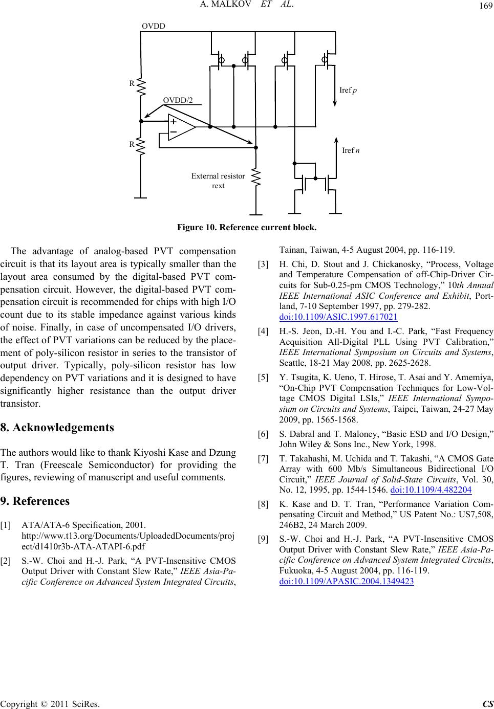 A. MALKOV ET AL. 169 OVDD/2 E xternal re sistor rext Iref p Iref n R R OVDD Figure 10. Reference current block. The advantage of analog-based PVT compensation circuit is that its layout area is typically smaller than the layout area consumed by the digital-based PVT com- pensation circuit. However, the digital-based PVT com- pensation circuit is recommended fo r chips with high I/O count due to its stable impedance against various kinds of noise. Finally, in case of uncompensated I/O drivers, the effect of PVT variations can be reduced by the place- ment of poly-silicon resistor in series to the transistor of output driver. Typically, poly-silicon resistor has low dependency on PVT variations and it is designed to have significantly higher resistance than the output driver transistor. 8. Acknowledgements The authors would like to thank Kiyoshi Kase and Dzung T. Tran (Freescale Semiconductor) for providing the figures, reviewing of manuscript and useful comments. 9. References [1] ATA/ATA-6 Specification, 2001. http://www.t13.org/Documents/UploadedDocuments/proj ect/d1410r3b-ATA-ATAPI-6.pdf [2] S.-W. Choi and H.-J. Park, “A PVT-Insensitive CMOS Output Driver with Constant Slew Rate,” IEEE Asia-Pa- cific Conference on Advanced System Integrated Circuits, Tainan, Taiwan, 4-5 August 2004, pp. 116-119. [3] H. Chi, D. Stout and J. Chickanosky, “Process, Voltage and Temperature Compensation of off-Chip-Driver Cir- cuits for Sub-0.25-pm CMOS Technology,” 10th Annual IEEE International ASIC Conference and Exhibit, Port- land, 7-10 September 1997, pp. 279-282. doi:10.1109/ASIC.1997.617021 [4] H.-S. Jeon, D.-H. You and I.-C. Park, “Fast Frequency Acquisition All-Digital PLL Using PVT Calibration,” IEEE International Symposium on Circuits and Systems, Seattle, 18-21 May 2008, pp. 2625-2628. [5] Y. Tsugita, K. Ueno, T. Hirose, T. Asai and Y. Amemiya, “On-Chip PVT Compensation Techniques for Low-Vol- tage CMOS Digital LSIs,” IEEE International Sympo- sium on Circuits and Systems, Taipei, Taiwan, 24-27 May 2009, pp. 1565-1568. [6] S. Dabral and T. Maloney, “Basic ESD and I/O Design,” John Wiley & Sons Inc., New York, 1998. [7] T. Takahashi, M. Uchida and T. Takashi, “A CMOS Gate Array with 600 Mb/s Simultaneous Bidirectional I/O Circuit,” IEEE Journal of Solid-State Circuits, Vol. 30, No. 12, 1995, pp. 1544-1546. doi:10.1109/4.482204 [8] K. Kase and D. T. Tran, “Performance Variation Com- pensating Circuit and Method,” US Patent No.: US7,508, 246B2, 24 March 2009. [9] S.-W. Choi and H.-J. Park, “A PVT-Insensitive CMOS Output Driver with Constant Slew Rate,” IEEE Asia-Pa- cific Conference on Advanced System Integrated Circuits, Fukuoka, 4-5 August 2004, pp. 116-119. doi:10.1109/APASIC.2004.1349423 Copyright © 2011 SciRes. CS |