

Paper Menu >>
Journal Menu >>
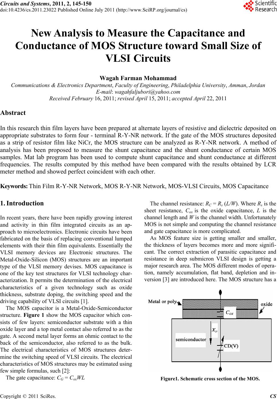 Circuits and Systems, 2011, 2, 145-150 doi:10.4236/cs.2011.23022 Published Online July 2011 (http://www.SciRP.org/journal/cs) Copyright © 2011 SciRes. CS New Analysis to Measure the Capacitance and Conductance of MOS Structure toward Small Size of VLSI Circuits Wagah Farman Mohammad Communications & Electronics Department, Faculty of Engineering, Philadelphia University, Amman, Jordan E-mail: [email protected] Received February 16, 2011; revised April 15, 2011; accepted April 22, 2011 Abstract In this research thin film layers have been prepared at alternate layers of resistive and dielectric deposited on appropriate substrates to form four - terminal R-Y-NR network. If the gate of the MOS structures deposited as a strip of resistor film like NiCr, the MOS structure can be analyzed as R-Y-NR network. A method of analysis has been proposed to measure the shunt capacitance and the shunt conductance of certain MOS samples. Mat lab program has been used to compute shunt capacitance and shunt conductance at different frequencies. The results computed by this method have been compared with the results obtained by LCR meter method and showed perfect coincident with each other. Keywords: Thin Film R-Y-NR Network, MOS R-Y-NR Network, MOS-VLSI Circuits, MOS Capacitance 1. Introduction In recent years, there have been rapidly growing interest and activity in thin film integrated circuits as an ap- proach to microelectronics. Electronic circuits have been fabricated on the basis of replacing conventional lumped elements with their thin film equivalents. Essentially the VLSI memory devices are Electronic structures. The Metal-Oxide-Silicon (MOS) structures are an important type of the VLSI memory devises. MOS capacitance is one of the key test structures for VLSI technology char- acterization. It permits the determination of the electrical characteristics of a given technology such as oxide thickness, substrate doping, the switching speed and the driving capability of VLSI circuits [1]. The MOS capacitor is a Metal-Oxide-Semiconductor structure. Figure 1 show the MOS capacitor which con- sists of few layers: semiconductor substrate with a thin oxide layer and a top metal contact also referred to as the gate. A second metal layer forms an ohmic contact to the back of the semiconductor, also referred to as the bulk. The electrical characteristics of MOS structures deter- mine the switching speed of VLSI circuits. The electrical characteristics of MOS structures may be estimated using few simple formulas, such [2]: The gate capacitance: CG = CoxWL The channel resistance: RC = Rs (L/W). Where Rs is the sheet resistance, Cox is the oxide capacitance, L is the channel length and W is the channel width. Unfortunately MOS is not simple and computing the channel resistance and gate capacitance is more complicated. As MOS feature size is getting smaller and smaller, the thickness of layers becomes more and more signifi- cant. The correct extraction of parasitic capacitance and resistance in deep submicron VLSI design is getting a major research area. The MOS different modes of opera- tion, namely accumulation, flat band, depletion and in- version [3] are introduced here. The MOS structure has a Figure1. Schematic cross section of the MOS. 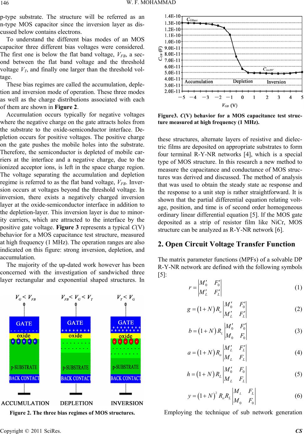 146 W. F. MOHAMMAD p-type substrate. The structure will be referred as an n-type MOS capacitor since the inversion layer as dis- cussed below contains electrons. To understand the different bias modes of an MOS capacitor three different bias voltages were considered. The first one is below the flat band voltage, VFB, a sec- ond between the flat band voltage and the threshold voltage VT, and finally one larger than the threshold vol- tage. These bias regimes are called the accumulation, deple- tion and inversion mode of operation. These three modes as well as the charge distributions associated with each of them are shown in Figur e 2. Accumulation occurs typically for negative voltages where the negative charge on the gate attracts holes from the substrate to the oxide-semiconductor interface. De- pletion occurs for positive voltages. The positive charge on the gate pushes the mobile holes into the substrate. Therefore, the semiconductor is depleted of mobile car- riers at the interface and a negative charge, due to the ionized acceptor ions, is left in the space charge region. The voltage separating the accumulation and depletion regime is referred to as the flat band voltage, VFB. Inver- sion occurs at voltages beyond the threshold voltage. In inversion, there exists a negatively charged inversion layer at the oxide-semiconductor interface in addition to the depletion-layer. This inversion layer is due to minor- ity carriers, which are attracted to the interface by the positive gate voltage. Figure 3 represents a typical C(V) behavior for a MOS capacitance test structure, measured at high frequency (1 MHz). The operation ranges are also indicated on this figure: strong inversion, depletion, and accumulation. The majority of the up-dated work however has been concerned with the investigation of sandwiched three layer rectangular and exponential shaped structures. In Figure 2. The three bias regimes of MOS structures. Figure3. C(V) behavior for a MOS capacitance test struc- ture measured at high frequency (1 MHz). these structures, alternate layers of resistive and dielec- tric films are deposited on appropriate substrates to form four terminal R-Y-NR networks [4], which is a special type of MOS structure. In this research a new method to measure the capacitance and conductance of MOS struc- tures was derived and discussed. The method of analysis that was used to obtain the steady state ac response and the response to a unit step is rather straightforward. It is shown that the partial differential equation relating volt- age, position, and time is of second order homogeneous ordinary linear differential equation [5]. If the MOS gate deposited as a strip of resistor film like NiCr, MOS structure can be analyzed as R-Y-NR network [6]. 2. Open Circuit Voltage Transfer Function The matrix parameter functions (MPFs) of a solvable DP R-Y-NR network are defined with the following symbols [5]: 00 L L M F r M F (1) 00 1o L L M F gNR M F (2) 00 00 1L M F bNR M F (3) 1 L L o L L M F aNR M F (4) 00 1L L L M F hNR M F (5) 2 00 1L L oL M F yNRR M F (6) Employing the technique of sub network generation Copyright © 2011 SciRes. CS 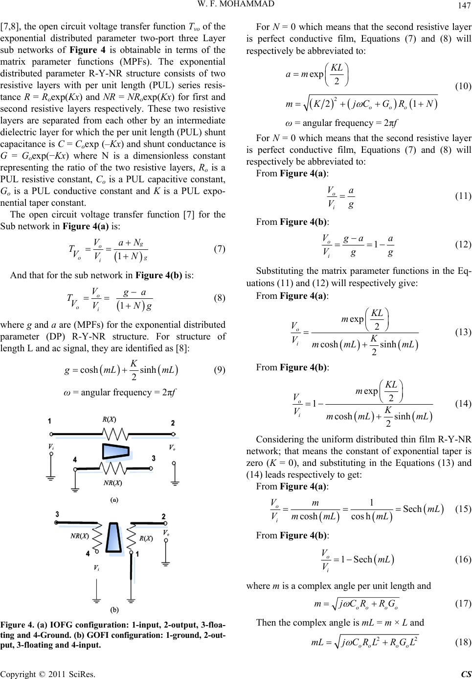 W. F. MOHAMMAD 147 [7,8], the open circuit voltage transfer function Tvo of the exponential distributed parameter two-port three Layer sub networks of Figure 4 is obtainable in terms of the matrix parameter functions (MPFs). The exponential distributed parameter R-Y-NR structure consists of two resistive layers with per unit length (PUL) series resis- tance R = Roexp(Kx) and NR = NRoexp( Kx) for first and second resistive layers respectively. These two resistive layers are separated from each other by an intermediate dielectric layer for which the per unit length (PUL) shunt capacitance is C = Coexp (–Kx) and shunt conductance is G = Goexp(−Kx) where N is a dimensionless constant representing the ratio of the two resistive layers, Ro is a PUL resistive constant, Co is a PUL capacitive constant, Go is a PUL conductive constant and K is a PUL expo- nential taper constant. The open circuit voltage transfer function [7] for the Sub network in Figure 4(a) is: 1 g o g oi VaN T VVN (7) And that for the sub network in Figure 4(b) is: 1 o oi V g a T VVN g (8) where g and a are (MPFs) for the exponential distributed parameter (DP) R-Y-NR structure. For structure of length L and ac signal, they are identified as [8]: cosh sinh 2 K g mL mL (9) ω = angular frequency = 2πf Figure 4. (a) IOFG configuration: 1-input, 2-output, 3-floa- ting and 4-Gr ound. (b) GOFI config uration: 1-grou nd, 2-out- put, 3-floating and 4-input. For N = 0 which means that the second resistive layer is perfect conductive film, Equations (7) and (8) will respectively be abbreviated to: 2 exp 2 21 ooo KL am mK jCGRN (10) ω = angular frequency = 2πf For N = 0 which means that the second resistive layer is perfect conductive film, Equations (7) and (8) will respectively be abbreviated to: From Figure 4(a): o i Va Vg (11) From Figure 4(b): 1 o i V g a Vg a g (12) Substituting the matrix parameter functions in the Eq- uations (11) and (12) will respectively give: From Figure 4(a): exp 2 cosh sinh 2 o i KL m V K VmmL mL (13) From Figure 4(b): exp 2 1 cosh sinh 2 o i KL m V K VmmL mL (14) Considering the uniform distributed thin film R-Y-NR network; that means the constant of exponential taper is zero (K = 0), and substituting in the Equations (13) and (14) leads respectively to get: From Figure 4(a): 1Sech coshcos h o i VmmL Vm mLmL (15) From Figure 4(b): 1 Sech o i VmL V (16) where m is a complex angle per unit length and oo oo mjCRRG (17) Then the complex angle is mL = m × L and 2 oo oo mLjCRLR GL 2 (18) Copyright © 2011 SciRes. CS 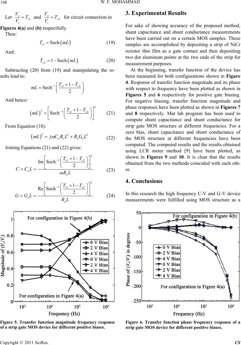 W. F. MOHAMMAD Copyright © 2011 SciRes. CS 148 3. Experimental Results Let 1 o v i VT V and 2 o v i VT V for circuit connection in For sake of showing accuracy of the proposed method, shunt capacitance and shunt conductance measurements have been carried out on a certain MOS samples. These samples are accomplished by depositing a strip of NiCr resistor thin film as a gate contact and then depositing two dot aluminum points at the two ends of the strip for measurement purposes. Figures 4(a) and (b) respectfully. Then: 1Sech v TmL mL (19) And: 21Sech v T (20) Subtracting (20) from (19) and manipulating the re- sults lead to: 112 1 Sech 2 vv TT mL And hence: 2 2112 1 Sech 2 vv TT mL 2 (21) From Equation (18): 22 oo oo mLjCRLR GL (22) Joining Equations (21) and (22) gives: 2 112 1 ImSech2 vv o o TT CCL RL (23) At the beginning, transfer function of the device has been measured for both configurations shown in Figure 4. Response of transfer function magnitude and its phase with respect to frequency have been plotted as shown in Figures 5 and 6 respectively for positive gate biasing. For negative biasing, transfer function magnitude and phase responses have been plotted as shown in Figures 7 and 8 respectively. Mat lab program has been used to compute shunt capacitance and shunt conductance for strip gate MOS structure at different frequencies. For a zero bias, shunt capacitance and shunt conductance of the MOS structure at different frequencies have been computed. The computed results and the results obtained using LCR meter method [9] have been plotted, as shown in Figures 9 and 10. It is clear that the results obtained from the two methods coincided with each oth- er. 2 112 1 Re Sech2 vv o o TT GGL RL (24) 4. Conclusions In this research the high frequency C-V and G-V device measurements were fulfilled using MOS structure as a Figure 5. Transfer function magnitude frequency response of a strip gate MOS device for different positive biases. Figure 6. Transfer function phase frequency response of a strip gate MOS device for different positive biases. 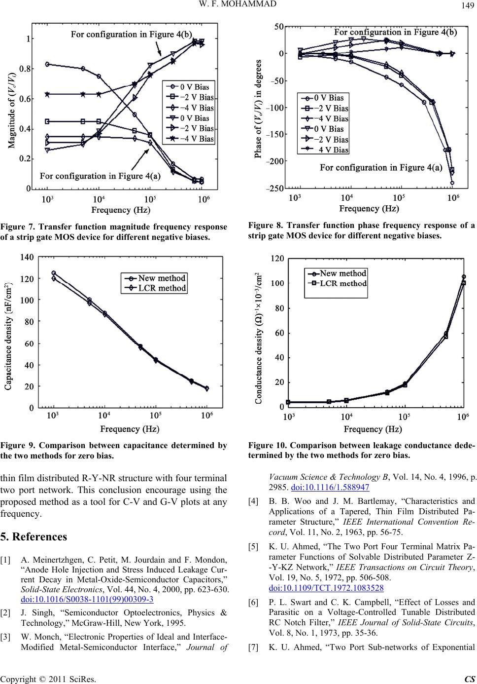 W. F. MOHAMMAD Copyright © 2011 SciRes. CS 149 Figure 7. Transfer function magnitude frequency response of a strip gate MOS device for different negative biases. Figure 8. Transfer function phase frequency response of a strip gate MOS device for different negative biases. Figure 9. Comparison between capacitance determined by the two methods for zero bias. Figure 10. Comparison between leakage conductance dede- termined by the two methods for zero bias. thin film distributed R-Y-NR structure with four terminal two port network. This conclusion encourage using the proposed method as a tool for C-V and G-V plots at any frequency. 5. References [1] A. Meinertzhgen, C. Petit, M. Jourdain and F. Mondon, “Anode Hole Injection and Stress Induced Leakage Cur- rent Decay in Metal-Oxide-Semiconductor Capacitors,” Solid-State Electronics, Vol. 44, No. 4, 2000, pp. 623-630. doi:10.1016/S0038-1101(99)00309-3 [2] J. Singh, “Semiconductor Optoelectronics, Physics & Technology,” McGraw-Hill, New York, 1995. [3] W. Monch, “Electronic Properties of Ideal and Interface- Modified Metal-Semiconductor Interface,” Journal of Vacuum Science & Technology B, Vol. 14, No. 4, 1996, p. 2985. doi:10.1116/1.588947 [4] B. B. Woo and J. M. Bartlemay, “Characteristics and Applications of a Tapered, Thin Film Distributed Pa- rameter Structure,” IEEE International Convention Re- cord, Vol. 11, No. 2, 1963, pp. 56-75. [5] K. U. Ahmed, “The Two Port Four Terminal Matrix Pa- rameter Functions of Solvable Distributed Parameter Z- -Y-KZ Network,” IEEE Transactions on Circuit Theory, Vol. 19, No. 5, 1972, pp. 506-508. doi:10.1109/TCT.1972.1083528 [6] P. L. Swart and C. K. Campbell, “Effect of Losses and Parasitic on a Voltage-Controlled Tunable Distributed RC Notch Filter,” IEEE Journal of Solid-State Circuits, Vol. 8, No. 1, 1973, pp. 35-36. [7] K. U. Ahmed, “Two Port Sub-networks of Exponential  150 W. F. MOHAMMAD Distributed Parameter Z-Y-KZ and Y-Z-KY Micro-cir- cuits with Similar Transfer Functions,” Micro Electron Reliable, Vol. 21, No. 2, 1981, pp. 235-239. [8] K. U. Ahmed, “A New Band-Reject Filter Configuration of Three-Layer Thin-Film Exponential R-C-KR,” Micro Electron Reliable, Vol. 21, No. 2, 1981, pp. 241-242. [9] P. Olivo, T. N. Nguyen and B. Ricco, “High-Field In- duced Degradation in Ultra-thin SiO2 Films,” IEEE Transactions on Electron Devices, Vol. 35, No. 12, 1988, pp. 2259-2267. doi:10.1109/16.8801 Copyright © 2011 SciRes. CS |