

Paper Menu >>
Journal Menu >>
 Circuits and Systems, 2011, 2, 139-144 doi:10.4236/cs.2011.23021 Published Online July 2011 (http://www.SciRP.org/journal/cs) Copyright © 2011 SciRes. CS Linearized Phase Detector Zero Crossing DPLL Performance Evaluation in Faded Mobile Channels Qassim Nasir1, Saleh Al-Araji2 1Department of Electrical and Computer Engineering, University of Sharjah, Sharjah, UAE 2Communication Engineering Department, Khalifa University of Science, Technology and Research, Sharjah, UAE E-mail: [email protected], [email protected] Received February 13, 2011; revised April 15, 2011; accepted April 22, 2011 Abstract Zero Crossing Digital Phase Locked Loop with Arc Sine block (AS-ZCDPLL) is used to linearize the phase difference detection, and enhance the loop performance. The loop has faster acquisition, less steady state phase error, and wider locking range compared to the conventional ZCDPLL. This work presents a Zero Crossing Digital Phase Locked Loop with Arc Sine block (ZCDPLL-AS). The performance of the loop is analyzed under mobile faded channel conditions. The mobile channel is assumed to be two path fading channel corrupted by additive white Gaussian noise (AWGM). It is shown that for a constant filter gain, the frequency spread has no effect on the steady state phase error variance when the loop is subjected to a phase step. For a frequency step and under the same conditions, the effect on phase error is minimal. Keywords: Non-uniform Sampling, Digital Phase Locked Loops, Zero Crossing DPLL, Mobile Faded Channels 1. Introduction Phase Lock Loops (PLLs) are used in a wider range of communication applications such as carrier recovery synchronization, and demodulation [1]. A PLL is a clo- sed loop system in which the phase output tracks the phase of the input signal. It consists of a phase detector, filter, and voltage controlled oscillator. Digital Phase locked Loops (DPLLs) were introduced to minimize some of the problems associated with the analogue counter part such as sensitivity to DC drift and the need for periodic adjustments [1,2]. Conventional Zero Cros- sing DPLL (ZCDPLL) is the most widely used due to its simplicity in modeling and implementation [3,4]. In this paper an Arc-Sine ZCDPLL is analyzed under mobile faded channel. The purpose of including the Arc- -Sine in the loop is to linearize the phase difference de- tection. The peak detector guarantees the input amplitude to the Arc-Sine block to remain between –1 and +1. It has been shown that the AS-ZCDPLL loop offers im- proved performance in the lock range and acquisition with reduced steady state phase error [5]. The proposed ZCDPLL-AS can be characterized by a linear difference equation in module (π/2) sense. The mobile radio channel is characterized by fast Ray- leigh fading and random phase distribution. This consid- erably degrades the tracking performance and increase the jitter of the loop. In this paper, the performance of ZCDPLL-AS with phase and frequency step inputs in the mobile radio environment is studied. The ZCDPLL-AS, in this work is considered as part of a mobile receiver. The mobile channel is assumed to be a two path fading channel corrupted by additive white Gaussian noise (AWGN). The fading in each path of the channel follows Rayleigh distribution and has power spectral density as given by Jakes [6]. 2 2 π1 m m Sf f ff where fm = vfc/c is the Doppler frequency that depends on the speed of the vehicle v and carrier frequency fc. The performance of the proposed algorithm will be evaluated for Doppler frequencies of 6 Hz, 100 Hz and 222 Hz, corresponding to a pedestrian (3.5 km/hr) and vehicular channels with speeds of 54 km/hr and 120 km/hr respectively. The stochastic difference equation describing the ZC- DPLL-AS loop operation is derived in Section 2. Finally,  140 1k Q. NASIR ET AL. the probability density function (pdf) of the steadys- tate phase error is derived and calculated numerically in Section 3. Experimental simulation results are presented in Section 4 and finally conclusion are given, in Section 5. 2. ZCDPLL-AS System Operation in Mobile Faded Channels The ZCDPLL-AS is composed of a sampler as a phase detector, inverse sine block, a digital loop filter, and a Digital Controlled Oscillator (DCO) as shown in Figure 1 [5]. The input signal to the loop is taken as x(t) = s1(t) + n(t) , where s1(t) is the noise free input signal to the loop after passing through the mobile channel. If s(t) = Asin(ω0t + θi(t)), n(t) is Additive white Gaussian Noise (AWGN); θi (t) = θ0+Ω0t , from which the signal dynam- ics are modeled; θ0 is the initial phase which we will assume to be zero; Ω0 is the frequency offset from the nominal value ω0. Then s1(t) = r(t)sin(ω0t + θi(t) + φch(t)), r(t) is Rayleigh faded envelope and φch(t), is a uniform distribution channel phase. The input signal is sampled at time instances tk deter- mined by the Digital Controlled Oscillator (DCO). The DCO period control algorithm as given by [7-10] is 01kkk TTc tt (1) where 0 2πT0 is the nominal period, 1k c is the output of the loop digital filter D(z). The sample value of the incoming signal x(t) at is k t 1kkk x tstnt (2) or kkk x sn (3) where k 0 sin kki s tt , The sequence k x is passed through the Arc-Sine block with output . The output is passed through a digital filter D(z) whose output is used to control the period of the DCO. 1 sin kk x k c y The time instances can be rewritten as k t 1 0 10 ,1,2,3, kk ki i ii tTkTck (4) Thus 1 00 , 0 sin k kki kchk k i x rwkT c n i i (5) The phase error is defined to be [5] 1 ,0 0 k kkchk i wc (6) Also 11,10 0 k kkchk i wc (7) D(z) DCO c k−1 t k x k−1 y k−1 x k S’(t) x(t) n(t) S(t) S / H Rayleigh faded Channel Peak Detector Register I ARC-SINE Bloc k Figure 1. Block diagram of the ZCDPLL-AS. Taking the difference of (7) and (8) results in 11,1,kkk kchkchk wc 0k (8) The Arc-Sine (1 sin ) block has been added to lin- earize the equation and avoid the nonlinear behaviour of the systems [5]. The output of the Arc-Sine block can be expressed as 1 kk xsinyk , and 11 k x π2yπ2 k . The z transform of the output of the digital filter is Cz DzYz (9) where Yz is the z transform of y t. The order of the loop is determined by the type of the digital filter. For first order, the digital filter is simply a gain block Dz 1 G , where is the block gain. However, for second order loop, 1 G 1 12 1z DzG G k . Let us consider a first order AS-ZCDPLL loop, then the digital filter output which controls the DCO is given by 1k cGy (10) Then the stochastic difference equation describing the loop behaviour is given by 11,1,01kkkkchkchk kkk wrGn (11) For phase step input where 1kk for , (11) becomes 0k 1,1,01kkchkchk kkk wrGn k (12) And for frequency step and for , (12) becomes 0k t 0k 1,1, 10 kkchkchk kkk wr GnT (13) In practical mobile communication systems and in the 800 MHz band, an IF frequency of 10.7 MHz is usually used; therefore, the sampling period T is on the order of 0.1 ps. The maximum Doppler frequency shift is on the order of 100 Hz (at vehicle velocity, about 60 mph). In other words, the ,1chk and ,ch k are equal, then (12) and (13) are reduced to Copyright © 2011 SciRes. CS  Q. NASIR ET AL. 141 1k1010kk kk k wrG wrGn (14) 11kkkkk wr GnT 0 k (15) For both cases, the probability density function of steady state phase error became a function of two inde- pendent random variables r(k) and n(k). 3. Phase Error Probability Density Function (pdf) 3.1. Phase Step without Noise In steady state 1k , (14) can be rewritten as 101 1 kk rG k (16) If the expected value of 01k is 1, then the ex- pected value of k wGr is zero for all values of k. This will lead to rapid convergence of the steady state. Since the probability density function of is Rayleigh then k r 2 2 2 2e, s k r r s r Pr r 0 (17) which has an average of π2 s . Therefore, the opti- mum value of the gain is 0 12π opt s G . Let b = , where , n is integer. Then the tran- sition pdf can be shown as to be 01 sinGz πzn 2 22 k+1 2 22 e. s k uz b s uz u P zb uz (18) 3.2. Phase Step plus Noise Let 01k yZ Gn be a Gaussian random variable with a mean of z and variance 222 01 n G ,where 2 n is the variance of the noise n(t). Then the pdf of y is given by 2 222 01 2 01 1e 2π n yz G y n Py G (19) So 10 ,sin kk 1 y brbw Gz (20) When 1 0, k z π,k zn will be zero mean Gaussian. Also when 1 will be Gaussian with mean of z. The transition pdf can be rewritten as [4] 2 222 01 1 π 2 01 1e π2π n kk un G n u PnG (21) Given kz , then 111 0 0 2π sin , kk k zGrzGn (22) Define a random variable Y as 10 0 2π k Yz Gn (23) Y will be Gaussian with mean 0 2π1z and variance 22 1n G . Therefore 2 0 222 1 2π1 2 1 1e 2 n yz G Y n Py G (24) 1 ', 'sin kk YbrbGz 1 (25) Since k is a discrete time continuous variable Mar- kov process, its conditioned on an initial condition error 0 satisfies Chapman-Kolmogrov equation, then 11 0 d kkkk z PPP z z (26) Equation (23) is valid whether k and 1k rare mutu- ally independent or not. This is solved numerically as was done in [4]. The transition pdf r P z is stored in a matrix starting with 000 zPz , 10 k P is calculated from 0 k P with k = 1,2,···, until the values of successive k differ by a prescribed small amount. 4. Simulation Results The performance of the loop was evaluated in simulation by subjecting it to phase as well as frequency steps. The input signal s(t) = sin(2000_t) is considered as modula- tion free and the DCO center frequency is 1000 Hz. In the simulation process, the Signal to Noise Ratio is de- fined as SNRdb = 10 2 log 1n , where 2 n represents noise variance. The loop is studied under phase step in the presence of noise. It is noticed from Figure 2, and as derived in section (2), that the steady state phase error variance depends on the value of the filter gain, as shown in Figure 3. The increase in gain causes the phase error to increase sharply which results in degradation in sys- tem’s performance. The effect of SNR on the phase error variance is shown in Figure 4. This variance is directly proportional to SNR as shown in Figure 5. As shown from the figure, the loop performance due to phase jitter improves as SNR increases. The frequency spread has no direct effect on the steady state phase error variance if the filter gain is kept constant, as shown in Figure 6. However, if the loop input signal is subjected to a fre- quency step, then the loop jitter is slightly affected by the Copyright © 2011 SciRes. CS  142 Q. NASIR ET AL. step size if the filter gain is kept constant. The Doppler spread will increase the jitter if the spread is increased as shown in Figure 6. The loop probability density function of the phase performance when subjected to a frequency step is shown in Figure 7 for different frequency offsets, while Figure 8 is for different wireless channel Doppler spreads. It is seen from the figures that the impact of frequency offset and channel speed of variations (Dop- pler spread) on the system performance is minimal. The loop performance, when a frequency step is applied to the loop, is also affected by the channel SNR as shown in Figure 9. The variance of timing error in the loop is in- creased as the loop gain G1 is increased and this primary- Figure 2. Probability Density Function (pdf) of DCO Period when SNR = 10 dB and when Phase step is applied with different values of filter gain G1. Figure 3. Variance of DCO period against filter gain G1. Figure 4. Probability Density Function (pdf) of DCO period for SNR = 10, 20 dB and when phase step is applied. Figure 5. Variance of DCO period versus input signal SNR. Figure 6. Probability Density Function (pdf) of DCO period for SNR = 20 dB with phase step with different doppler spreads. Copyright © 2011 SciRes. CS 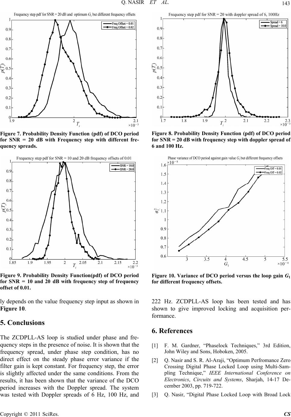 Q. NASIR ET AL. Copyright © 2011 SciRes. CS 143 Figure 8. Probability Density Function (pdf) of DCO period for SNR = 20 dB with frequency step with doppler spread of 6 and 100 Hz. Figure 7. Probability Density Function (pdf) of DCO period for SNR = 20 dB with Frequency step with different fre- quency spre a ds. Figure 9. Probability Density Function(pdf) of DCO period for SNR = 10 and 20 dB with frequency step of frequency offset of 0.01. Figure 10. Variance of DCO period versus the loop gain G1 for different frequency offsets. ly depends on the value frequency step input as shown in Figure 10. 5. Conclusions The ZCDPLL-AS loop is studied under phase and fre- quency steps in the presence of noise. It is shown that the frequency spread, under phase step condition, has no direct effect on the steady phase error variance if the filter gain is kept constant. For frequency step, the error is slightly affected under the same conditions. From the results, it has been shown that the variance of the DCO period increases with the Doppler spread. The system was tested with Doppler spreads of 6 Hz, 100 Hz, and 222 Hz. ZCDPLL-AS loop has been tested and has shown to give improved locking and acquisition per- formance. 6. References [1] F. M. Gardner, “Phaselock Techniques,” 3rd Edition, John Wiley and Sons, Hoboken, 2005. [2] Q. Nasir and S. R. Al-Araji, “Optimum Perfromance Zero Crossing Digital Phase Locked Loop using Multi-Sam- pling Technique,” IEEE International Conference on Electronics, Circuits and Systems, Sharjah, 14-17 De- cember 2003, pp. 719-722. [3] Q. Nasir, “Digital Phase Locked Loop with Broad Lock 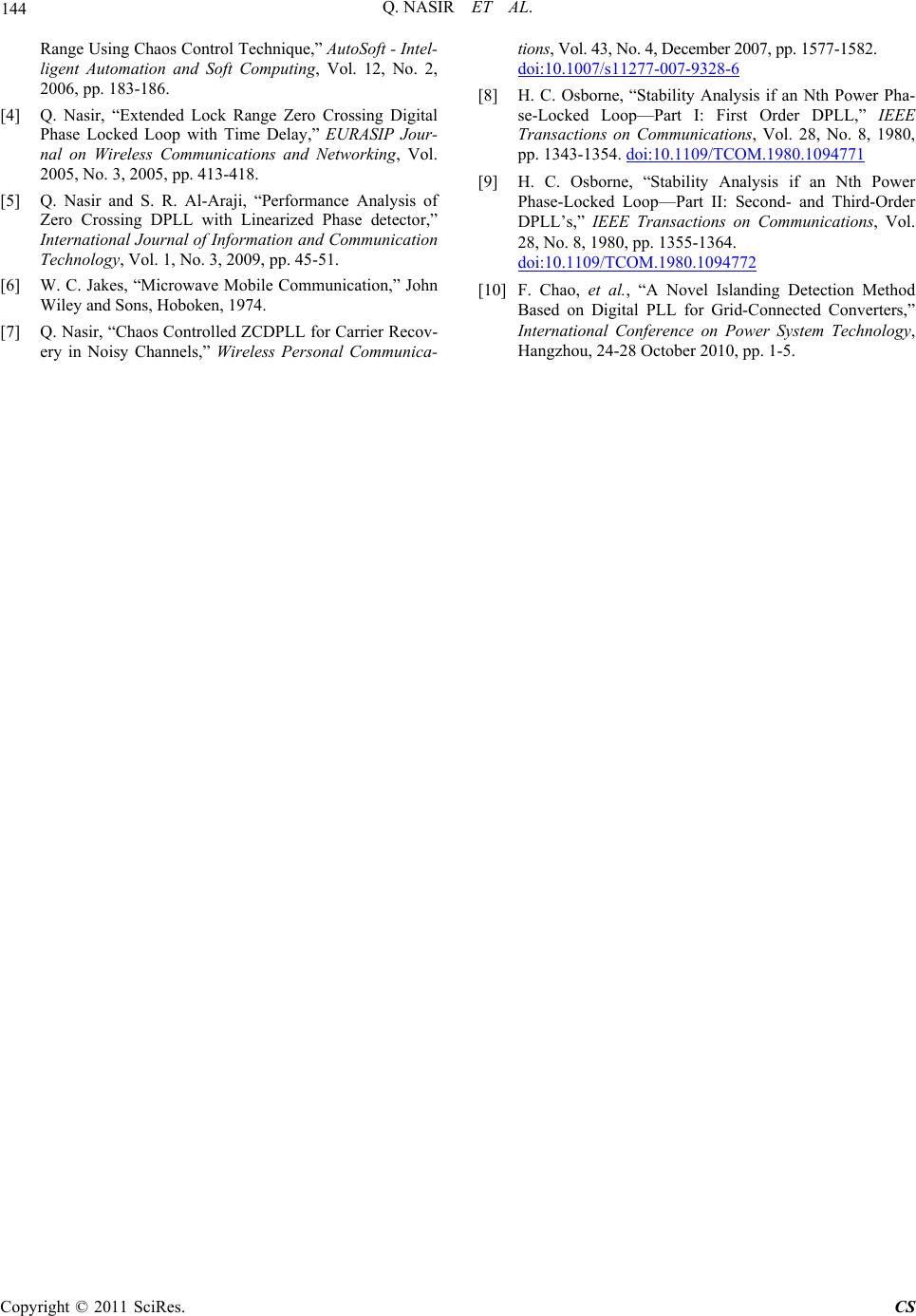 144 Q. NASIR ET AL. Range Using Chaos Control Technique,” AutoSoft - Intel- ligent Automation and Soft Computing, Vol. 12, No. 2, 2006, pp. 183-186. [4] Q. Nasir, “Extended Lock Range Zero Crossing Digital Phase Locked Loop with Time Delay,” EURASIP Jour- nal on Wireless Communications and Networking, Vol. 2005, No. 3, 2005, pp. 413-418. [5] Q. Nasir and S. R. Al-Araji, “Performance Analysis of Zero Crossing DPLL with Linearized Phase detector,” International Journal of Information and Communication Technology, Vol. 1, No. 3, 2009, pp. 45-51. [6] W. C. Jakes, “Microwave Mobile Communication,” John Wiley and Sons, Hoboken, 1974. [7] Q. Nasir, “Chaos Controlled ZCDPLL for Carrier Recov- ery in Noisy Channels,” Wireless Personal Communica- tions, Vol. 43, No. 4, December 2007, pp. 1577-1582. doi:10.1007/s11277-007-9328-6 [8] H. C. Osborne, “Stability Analysis if an Nth Power Pha- se-Locked Loop—Part I: First Order DPLL,” IEEE Transactions on Communications, Vol. 28, No. 8, 1980, pp. 1343-1354. doi:10.1109/TCOM.1980.1094771 [9] H. C. Osborne, “Stability Analysis if an Nth Power Phase-Locked Loop—Part II: Second- and Third-Order DPLL’s,” IEEE Transactions on Communications, Vol. 28, No. 8, 1980, pp. 1355-1364. doi:10.1109/TCOM.1980.1094772 [10] F. Chao, et al., “A Novel Islanding Detection Method Based on Digital PLL for Grid-Connected Converters,” International Conference on Power System Technology, Hangzhou, 24-28 October 2010, pp. 1-5. Copyright © 2011 SciRes. CS |