

Paper Menu >>
Journal Menu >>
 Journal of Encapsulation and Adsorption Sciences, 2011, 1, 23-28 doi:10.4236/jeas.2011.11003 Published Online June 2011 (http://www.scirp.org/journal/jeas) Copyright © 2011 SciRes. JEAS New Organic Thin-Film Encapsulation for Organic Light Emitting Diodes Rakhi Grover1,2, Ritu Srivastava1, Omwati Rana1, D. S. Mehta2, M. N. Kamalasanan1 1Center for Organic Electronics, Physics of Energy Harvesting Division, National Physical Laboratory (Council of Scientific and Industrial Research), New Delhi, India 2Instrument Design Development Center, Indian Institute of Technology Delhi, New Delhi, India E-mail: [email protected] Received March 11, 2011; revised April 12, 2011; accepted April 20, 2011 Abstract Organic Light-Emitting diodes (OLEDs) are extremely sensitive to water vapour and oxygen, which causes rapid degradation. Epoxy and cover glass with large amount of desiccant are commonly applied to encapsu- late bottom emitting OLEDs which is not a viable option for flexible as well as top emitting OLEDs. This paper reports a completely organic encapsulating layer consisting of four periods of alternate stacks of two organic materials with different morphologies deposited by simple vacuum thermal evaporation technique. Standard green OLED structures with and without encapsulation were fabricated and investigated using structural, optical and electrical studies. Moreover, the encapsulation presented being organic is safe for un- derlying organic layers in OLEDs and is ultrathin, transparent and without any cover glass and desiccant, ensuring its application in flexible and top emitting OLEDs. Keywords: OLED, Thin Film Encapsulation, Diffusion Barrier, Atomic Force Microscopy 1. Introduction Organic Light-Emitting diodes (OLEDs) are considered as one of the most potential display technology today due to their low power consumption, low cost, and superior viewing ability [1] especially for their possibility to build flexible displays [2-6] as they are ultra-thin and light weight. Top emitting OLED devices are also becoming increasingly important because of the increase in aper- ture ratio (the ratio of actual emitting area to the total area of the pixel) obtained as compared to bottom emitter approach. However one obstacle to these developments is the susceptibility of these devices to water vapor and oxygen, which causes rapid degradation. Device reliability issues, in part, arise due to the envi- ronmental instability of both the active materials and low work function electrode in the devices [7-11]. Low work function metals are highly reactive with oxygen and wa- ter vapor and, thus, oxidize very quickly. This results in the formation of insulating oxide barriers, making the injection and collection of charge carriers less efficient. Exposure to water vapor and oxygen in the environment may also result in the formation of black spots in OLEDs, reducing their light output and lifetimes [12]. Another detrimental degradation mechanism which can arise from environmental-induced oxidation is the delamination within the device. When water vapor permeates through defects into the interface formed by the cathode and an active layer, it may cause chemical reactions which in- duce out gassing or volumetric expansion leading to de- lamination [13,14]. A number of approaches to encapsulation have been developed including the use of metal lids, glass and the sealing of devices between two glass substrates or plastic substrates treated with barrier films [15,16]. Additionally, getter materials such as calcium and barium are used to remove any residual water in the encapsulated volume or water vapour which diffuses through the epoxy sealant [17]. However, these rigid materials are not amenable for use in flexible OLEDs which require flexible covering as well as for top emitting OLEDs in which the emitted light has to pass through the cover glass and the opaque desiccant. Therefore Thin Film Encapsulation (TFE) technology is the key technique to meet the requirements of small-size flexible and top emitting electronic display devices. For active layers and substrates with low glass- transition temperatures and thermal stability, the proc-  R. GROVER ET AL. 24 essing temperatures at which the barrier layers can be deposited should be low. However, processing at low temperature may lead to more defects in the films, limit- ing the overall barrier performance. Therefore, inorganic films are limited in their performance mainly due to the presence of defects in the films which provide pathways for water vapour and oxygen to permeate through the barrier layers. By applying multilayer films with alternating stacks, defects which span the entire thickness of the individual inorganic layers are interrupted and do not channel con- tinuously through the film structure. This structure cre- ates a tortuous path resulting in very long effective diffu- sion pathways, increasing the barrier performance (“de- fect interruption layer”) [18]. These results suggest that developing ultra-high barrier performance encapsulation layer as well as more stable materials for organic device is important for extended lifetime of organic devices. Also, the deposition techniques of these inorganic mate- rials can damage the underlying sensitive organic layers used in OLEDs. Thus, the development and integration of high-barrier encapsulation films with organic elec- tronics remains a challenging endeavour. The focus of the present work is to prepare completely organic thin film encapsulation for OLEDs which has been demonstrated by combining alternate stacks of two differ- ent organic materials having different morphologies and different thin film forming properties. One of the organic material chosen is TPD (TPD-N, N’-diphenyl-N, N’-bis-3 -methylphenyl [1, 1’-bipheny]-4, 4’-diamine which is well known as hole transporting material in OLEDs but also known to get easily crystallized because of its low glass transition temperature (Tg = 64˚C). Another organic mate- rial chosen is newly synthesized material XP (2.2.6. 5, 5′-(4, 4′-(2,6-di-tert-butylanthracene-9,10-diyl)bis(4,1-phenyle ne))bis(2-(4-hexylphenyl)-1, 3, 4-oxadiazole) [19] having highly amorphous and stable thin film forming ability with a quite high glass transition temperature of 108˚C. Alter- nate stacks of thin layers of these materials have been fab- ricated and studied using Atomic force microscopy and Calcium corrosion test involving UV-Visible absorption spectroscopy. Finally the OLED devices with the opti- mized encapsulation showed enhanced lifetime as com- pared to the devices with no encapsulation layers. 2. Experimental Plain glass plates were used as the starting substrates and cleaned sequentially using de ionized water, acetone, tri- chloroethylene and isopropyl alcohol for 20 minutes each using an ultrasonic bath and then dried in vacuum oven. Thin films of Ca (Calcium), TPD and XP were deposited with thicknesses of 250 nm, 20 nm and 10 nm respectively under a high vacuum (10−5 - 10−6 Torr).The correspond- ing device structures being (also shown in Figure 2): (a) Glass/Ca (b) Glass/Ca/TPD (c) Glass/Ca/TPD/XP The thicknesses of these films were measured in situ by a quartz crystal thickness monitor. Morphological properties were examined using Atomic force micros- copy (AFM) (NT-MDT). UV-Vis spectra were taken using a high resolution UV-Vis spectrophotometer (Shi- madzu 2401 PC) in the range of 200 - 800 nm. Then OLEDs were fabricated incorporating the opti- mized encapsulation layer. Indium-tin oxide (ITO) (thi- ckness of 120 nm) coated glass plates with a sheet resis- tance of 20 Ω/□ (Vin Karola, USA) were used as starting substrates and were patterned and cleaned using deion- ised water, acetone, trichloroethylene and isopropyl al- cohol sequentially for 20 min each using an ultrasonic bath and dried in vacuum.The device structure of OLEDs grown by vacuum thermal deposition was: ITO/m-MTDATA (20 nm)/α-NPD (10 nm)/CBP +5% Ir (ppy)3 (35 nm)/TPBi (30 nm) /LiF (1 nm)/Al (200 nm). 4, 4’, 4”-tris(3-methyl-phenylphenylamino) triphenyl- amine (m-MTDATA) and N, N’-di-1-naphthalenyl-N, N’- diphenyl-1.1’ biphenyl-4, 4’-diamine (α-NPD) were used as hole injection and hole transporting layers re- spectively. 5% (Ir (ppy)3) doped (CBP) was used as the emissive layer. 2, 2’, 2’’-(l, 3, 5-benzenetriyl)-tris (L-ph- enyl-l-H-benzimidazole (TPBi) and LiF were used as electron transporting and electron injection layers re- spectively. The size of each pixel was 5 mm 5 mm. Then four periods of TPD (20 nm)/XP (10 nm) layers were deposited. The current density-voltage-luminesc- ence (J-V-L) characteristics have been measured with a luminance meter (LMT-1009) interfaced with a Keithley 2400 programmable current-voltage digital source meter. All the measurements were carried out at room tempera- ture under ambient conditions. 3. Results and Discussion 3.1. Structural Studies Figure 1 shows the morphology of the thin films of XP as recorded from AFM with time .The films were found to be highly amorphous and more significantly stable also. As explained in Section 1, densely packed, continuous, and highly conformal coatings are desir- able for excellent barrier properties, so that all small particles are well encapsulated. Table 1 shows the av- erage roughness values of the thin film of XP with time and corresponding AFM images are presented in Fig- ure 1. Copyright © 2011 SciRes. JEAS 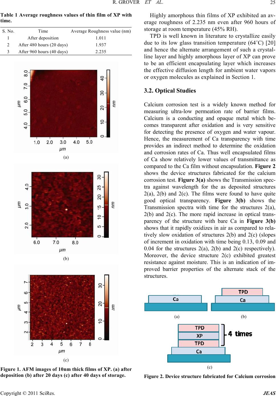 R. GROVER ET AL.25 Table 1 Average roughness values of thin film of XP with time. S. No. Time Average Roughness value (nm) 1 After deposition 1.011 2 After 480 hours (20 days)1.937 3 After 960 hours (40 days)2.235 (a) (b) (c) Figure 1. AFM images of 10nm thick films of XP. (a) after deposition (b) after 20 days (c) after 40 days of storage. Highly amorphous thin films of XP exhibited an av- erage roughness of 2.235 nm even after 960 hours of storage at room temperature (45% RH). TPD is well known in literature to crystallize easily due to its low glass transition temperature (64˚C) [20] and hence the alternate arrangement of such a crystal- line layer and highly amorphous layer of XP can prove to be an efficient encapsulating layer which increases the effective diffusion length for ambient water vapors or oxygen molecules as explained in Section 1. 3.2. Optical Studies Calcium corrosion test is a widely known method for measuring ultra-low permeation rate of barrier films. Calcium is a conducting and opaque metal which be- comes transparent after oxidation and is very sensitive for detecting the presence of oxygen and water vapour. Hence, the measurement of Ca transparency with time provides an indirect method to determine the oxidation and corrosion rates of Ca. Thus well encapsulated films of Ca show relatively lower values of transmittance as compared to the Ca film without encapsulation. Figure 2 shows the device structures fabricated for the calcium corrosion test. Figure 3(a) shows the Transmission spec- tra against wavelength for the as deposited structures 2(a), 2(b) and 2(c). The films were found to have quite good optical transparency. Figure 3(b) shows the Transmission spectra with time for the structures 2(a), 2(b) and 2(c). The more rapid increase in optical trans- parency of the structure with bare Ca in Figure 3(b) shows that it rapidly oxidizes in air as compared to rela- tively slow oxidation of structures 2(b) and 2(c) (slopes of increment in oxidation with time being 0.13, 0.09 and 0.04 for the structures 2(a), 2(b) and 2(c) respectively). Moreover, the device structure 2(c) exhibited greatest resistance against moisture. This is an indication of im- proved barrier properties of the alternate stack of the structures. (a) (b) (c) Figure 2. Device structure fabricated for Calcium corrosion Copyright © 2011 SciRes. JEAS 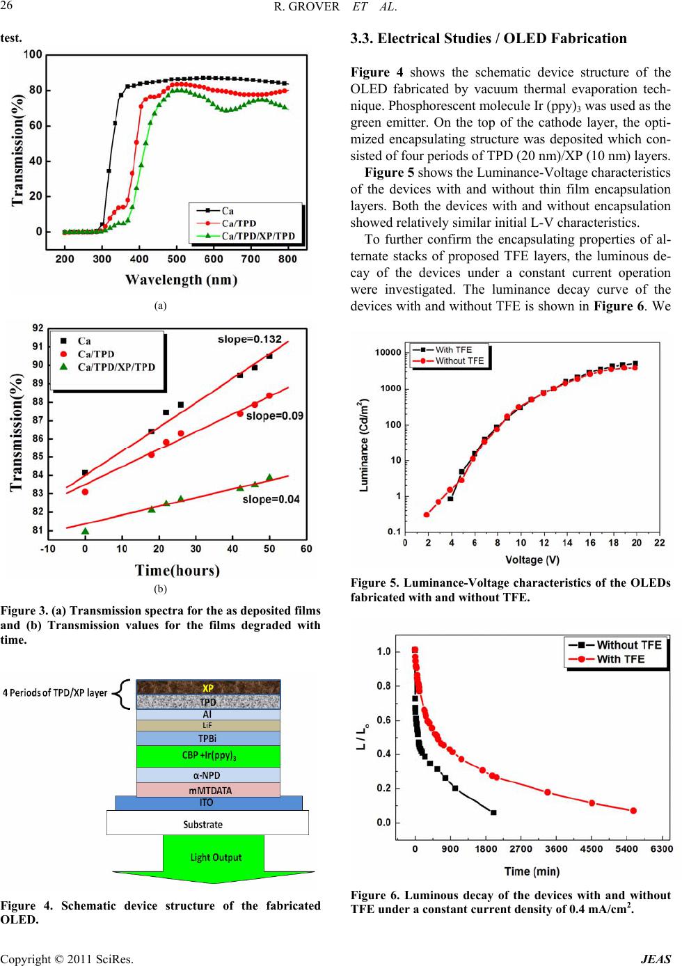 R. GROVER ET AL. 26 test. (a) (b) Figure 3. (a) Transmission spectra for the as deposited films and (b) Transmission values for the films degraded with time. Figure 4. Schematic device structure of the fabricated OLED. 3.3. Electrical Studies / OLED Fabrication Figure 4 shows the schematic device structure of the OLED fabricated by vacuum thermal evaporation tech- nique. Phosphorescent molecule Ir (ppy)3 was used as the green emitter. On the top of the cathode layer, the opti- mized encapsulating structure was deposited which con- sisted of four periods of TPD (20 nm)/XP (10 nm) layers. Figure 5 shows the Luminance-Voltage characteristics of the devices with and without thin film encapsulation layers. Both the devices with and without encapsulation showed relatively similar initial L-V characteristics. To further confirm the encapsulating properties of al- ternate stacks of proposed TFE layers, the luminous de- cay of the devices under a constant current operation were investigated. The luminance decay curve of the devices with and without TFE is shown in Figure 6. We Figure 5. Luminance-Voltage characteristics of the OLEDs fabricated with and without TFE. Figure 6. Luminous decay of the devices with and without TFE under a constant current density of 0.4 mA/cm2. Copyright © 2011 SciRes. JEAS  R. GROVER ET AL.27 have measured luminance of the devices at a continuous constant current of 0.4 mA/cm2, which gave an initial luminance of 140 Cd/m2 .As shown in Figure 6, the en- capsulated device, could stay longer (12 hours) as com- pared to the device without encapsulation layer (1.1 hours). The enhancement in lifetime of encapsulated device being around ten times higher than that of the device without encapsulation. Further studies on the work are in progress. Although the obtained device life- times are quite low in terms of efficient organic displays but can be enhanced due to fact that encapsulation layers were deposited without any further capping of the device as reported in literature with additional aluminium foil capping [21]. It is worth noting that the alternate stacking type encapsulation is ultrathin, optically transparent and flexible, suiting the encapsulation of flexible OLEDs as well as top emitting OLEDs. The barrier properties of the proposed TFE have been attributed to the defect interruption due to different types of film forming abilities of TPD and XP layers. TPD is well known to have a glass transition temperature as low as 64˚C whereas the newly synthesized material XP has a high glass transition temperature of 108˚C. The alternate stacks of these different types of films one highly amor- phous and other crystalline basically increase the diffu- sion lengths of ambient oxygen or water vapours thereby protecting the device. Additionally the TFE being or- ganic in nature can be deposited at much lower tempera- tures as compared to earlier reported inorganic encapsu- lation layers [22,23] and is therefore more compatible with the organic transport and emissive layers used in the organic based devices. Thus use of ultra-thin vacuum thermally-deposited alternate organic thin films is effec- tive as a barrier layer for significantly increasing the life- time of an OLED device. 4. Conclusions The encapsulation of an OLED device with the alternate stacks of two organic thin films TPD and XP with dif- ferent morphologies and different thin film forming properties using the vacuum thermal evaporation method has been carried out for the first time. Vacuum thermally deposited organic films showed excellent barrier proper- ties. The TFE was found to significantly slow down the oxygen and moisture diffusion into the device leading to a longer operational lifetime. 5. Acknowledgement The authors wish to acknowledge the Director, NPL, Delhi and Dr. S. S. Bawa for suggestions and discussions. The authors would like to acknowledge Department of Science and Technology DST and Council of Scientific and Industrial Research CSIR, New Delhi, India for fi- nancial support. 6. References [1] S. R. Forrest, “The Road to High Efficiency Organic Light Emitting Devices,” Organic Electronics, Vol. 4, No. 2-3, 2003, pp. 45-48. doi:10.1016/j.orgel.2003.08.014 [2] P. E. Burrows, G. L. Graff, M. E. Gross, P. M. Martin, M. K. Shi, M. Hall, E. Mast, C. Bonham, W. Bennet and M. B. Sullivan, “Ultra Barrier Flexible Substrates for Flat Panel Displays,” Displays, Vol. 22, No. 2, 2001, pp. 65-69. doi:10.1016/S0141-9382(00)00064-0 [3] G. Gu, P. E. Burrows, S. Venkatesh, et al., “Vacuum Deposited Nonpolymeric Flexible Organic Light Emitting Devices,” Optics Letters, Vol. 22, No. 3, 1997, pp. 172-174. doi:10.1364/OL.22.000172 [4] A. Kunio, M. Atsushi, F. Hisayoshi, et al., “Flexible Oled for Automobiles Using Sinx/Cnx:H Multi-Layer Barrier Films and Epoxy Substrates,” Journal of Photopolymer Science and Technology, Vol. 19, No. 2, 2006, pp. 203-208. doi:10.2494/photopolymer.19.203 [5] L. D. Wang, Y. Li, C. Chang, et al., “Research on the Adhesive Ability between ITO Anode and PET Substrate Improved by Polyimide Buffer Layer,” Chinese Science Bulletin, Vol. 50, No. 1, 2005, pp. 1-4. [6] Y. Qiu, L. Duan and L. D. Wang, “Flexible Organic Light-Emitting Diodes with Poly-3, 4-Ethylene-Dioxy- thiophene as Transparent Anode,” Chinese Science Bulle- tin, Vol. 47, No. 23, 2002, pp. 1979-1982. doi:10.1360/02tb9429 [7] J. Shen, D. Wang, E. Langlois, W. A. Barrow, P. J. Green and C. W. Tang, “Degradation Mechanism in Organic Light Emitting Diodes,” Synthetic Metals, Vol. 111-112, 2000, pp. 233-236. doi:10.1016/S0379-6779(99)00370-7 [8] S. T. Lee, Z. Q. Gao and L. S. Hung, “Metal Diffusion From Electrodes in Organic Light Emitting Diodes,” Ap- plied Physics Letters, Vol. 75, No. 10, 1999, pp. 1404-1406. doi:10.1063/1.124708 [9] Z. D. Popovic, H. Aziz, N. X. Hu, A. M. Hor and G. Xu, “Long-Term Degradation Mechanism of Tris (8-Hydrox- yq-Uinoline) Aluminium-Based Organic Light-Emitting Devices,” Synthetic Metals, Vol. 111-112, 2000, pp. 229-232. doi:10.1016/S0379-6779(99)00353-7 [10] Y. C. Luo, H. Aziz, Z. D. Popovic and G. Xu, “Degrada- tion Mechanisms in Organic Light-Emitting Devices: Metal Migration Model versus Unstable Tris (8-Hydroxy- quinoline) Aluminium Cationic Model,” Journal of Ap- plied Physics, Vol. 101, 2007, pp. 034510-1-4. [11] H. Aziz and Z. D. Popovic, “Degradation Phenomena in Small-Molecule Organic Light-Emitting Devices,” Chem- istry of Materials, Vol. 16, No. 23, 2004, pp. 4522-4532. doi:10.1021/cm040081o [12] D. Kolosov, D. S. English, V. Bulovic, P. F. Barbara, S. R. Forrest and M. E. Thompson, “Direct Observation of Structural Changes in Organic Light Emitting Devices Copyright © 2011 SciRes. JEAS  R. GROVER ET AL. Copyright © 2011 SciRes. JEAS 28 During Degradation,” Journal of Applied Physics, Vol. 90, No. 7, 2001, pp. 3242-3247. doi:10.1063/1.1389760 [13] H. Aziz, Z. Popovic, S. Xie, A. M. Hor, N. X. Hu, C. Tripp and G. Xu, “Humidity-Induced Crystallization of Tris (8-Hydroxyquinoline)Aluminum Layers in Organic Light-Emitting Devices,” Applied Physics Letters, Vol. 72, No. 7, 1997, pp. 756-758. doi:10.1063/1.120867 [14] M. Schaer, F. Niisch, D. Berner, W. Leo and L. Zuppiroli, “Water Vapor and Oxygen Degradation Mechanisms in Organic Light Emitting Diodes,” Advanced Functional Materials, Vol. 11, No. 2, 2001, pp. 116-121. doi:10.1002/1616-3028(200104)11:2<116::AID-ADFM1 16>3.0.CO;2-B [15] A. P. Ghosh, L. J. Gerenser, C. M. Jarman and J. E. For- nalik, “Thin-Film Encapsulation of Organic Light-Emitt- ing Devices,” Applied Physics Letters, Vol. 86, No. 22, 2005, pp. 223503-1-3. doi:10.1063/1.1929867 [16] M. S. Weaver, L. A. Michalski, K. Rajan, M. A. Rothman, J. A. Silvernail, J. J. Brown, P. E. Burrows, G. L. Graff, M. E. Gross, P. M. Martin, M. Hall, E. Mast, C. Bohnam, W. Bennett and M. Zurnhoff, “Organic Light-Emitting Devices with Extended Operating Lifetimes on Plastic Substrates,” Applied Physics Letters, Vol. 81, No. 16, 2002, pp. 2929-2931. doi:10.1063/1.1514831 [17] J. S. Lewis and M. S. Weaver, “Thin-Film Permea- tion-Barrier Technology for Flexible Organic Light-Emit- ting Devices,” IEEE Journal of Selected Topics in Quan- tum Electronics, Vol. 10, No. 1, 2004, pp. 45-57. doi:10.1109/JSTQE.2004.824072 [18] J. D. Affinito, M. E. Gross, C. A. Coronado, G. L. Graff, I. N. Greenwell and P. M. Martin, “A New Method for Fabricating Transparent Barrier Layers,” Thin Solid Films, Vol. 290-291, 1996, pp. 63-67. doi:10.1016/S0040-6090(96)09202-4 [19] M. A. Reddy, G. Mallesham, A. Thomas, K. Srinivas, V. J. Rao, K. Bhanuprakash, L. Giribabu, R. Grover, A. Kumar, M. N. Kamalasanan and R. Srivastava, “Synthe- sis and Characterization of Novel 2, 5-Diphenyl-1, 3, 4- Oxadiazole Derivatives of Anthracene and its Application in Electron Transporting Blue Emitters in Oleds,” Syn- thetic Metals, In Press. [20] K. Yamashita, T. Mori, T. Mizutani, H. Miyazaki and T. Takeda, “El Properties of Organic Light-Emitting-Diode Using TPD Derivatives with Diphenylstylyl Groups as Hole Transport Layer,” Thin Solid Films, Vol. 363,No. 1-2, 2000, pp. 33-36. doi:10.1016/S0040-6090(99)00977-3 [21] L. Song, Z. D. Qiang, L. Yang, D. Lian, D. Guifang, W. Liduo and Q. Yong, “New Hybrid Encapsulation for Flexible Organic Light-Emitting Devices on Plastic Sub- strates,” Chinese Science Bulletin, Vol. 53, No. 6, pp. 958-960. [22] J. Meyer, D. Schneidenbach, T. Winkler, S. Hamwi, T. Weimann, P. Hinze, S. Ammermann, H. -H. Johannes, T. Riedl and W. Kowalsky, “Reliable Thin Film Encapsula- tion for Organic Light Emitting Diodes Grown by Low- Temperature Atomic Layer Deposition,” Applied Physics Letters, Vol. 94, No. 23, 2009, pp. 233305-1-3. doi:10.1063/1.3153123 [23] S. -H. K. Park, J. -I. Lee, Y. S. Yang and S. J. Yun, “Characterization of Aluminum Oxide Thin Film Grown by Atomic Layer Deposition for Flexible Display Barrier Layer Application,” Proceedings of the 2nd Int’l Meet- ings Information Display, 2002, pp. 746-749. |