 Journal of Computer and Communications, 2014, 2, 41-48 Published Online November 2014 in SciRes. http://www.scirp.org/journal/jcc http://dx.doi.org/10.4236/jcc.2014.213006 How to cite this paper: Espinosa, C.A.L. (2014) State Variable Model for Considering the Parasitic Inductor Resistance on the Open Loop Performance of DC to DC Converters. Journal of Computer and Communications, 2, 41-48. http://dx.doi.org/10.4236/jcc.2014.213006 State Variable Model for Considering the Parasitic Inductor Resistance on the Open Loop Performance of DC to DC Converters Carlos Alberto Lozano Espinosa Pontificia Universidad Javeriana, Santiago de Cali, Colombia Received 17 October 2014 Abstract This paper shows DC and small-signal circuit models for the PWM DC to DC bu c k, bo ost and back/ boost con ver te rs wi th the equivalent series resistance of the inductor. The DC voltage transfer function and the efficiency of the converter are derived from the DC model. Small-signal open-loop characteristics are derived from the small-signal model based on a state variable model. A design example proves the performance of the circuit and verification of the model. Keywords DC to DC Con verte r, Parasitic Resistance of Inductor, Small Signal Analysis, Bu ck Conv erter , Boos t Converter, Buck-Boost Conver ter 1. Introduction Many papers about small signal analysis of a DC to DC b uc k-boost converter can be found in literature that in- clude parasitic resistances in inductor and capacitors and voltage drop in power switch and diode [1]-[5]. Usual- ly, the signal model representation is obtained from an equivalent circuit [4], or in other cases, using a state va- riable model [3]. Any model can be calculated based on the continuous conduction mode or a non-continuous conduction mode but have different results because the former has control over the duty cycle and the latter has control over the frequency. The objectives of this paper are: to obtain a DC and small-signal linear circuit models of PWM buc k, boost and buck/boost DC-DC converter, taking into account parasitic resistance of the inductor; to derive the DC vol- tage transfer function and efficiency; to derive small-signal open-loop input-to-output transfer function using a state variable model; and to demonstrate, by a design consideration, the performance of a real circuit. 2. Work Description In anon ideal DC to DC converter, it is necessary to consider power losses from parasitic resistance of the in- ductor, parasitic resistance of capacitors and power losses in semiconductor switch and diode. Figure 1 shows some real DC to DC converters with parasitic resistance in inductor. 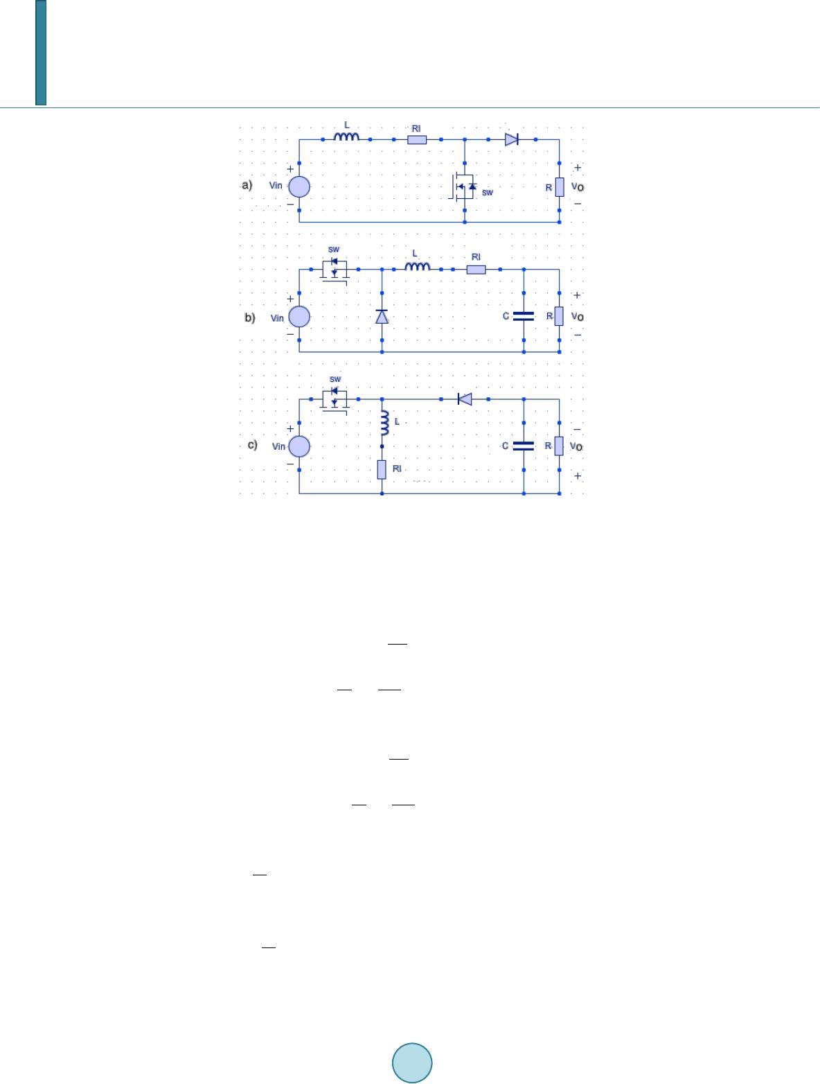 C. A. L. Espinosa Figure 1. DC to DC Converters: (a) Boost; (b) Buc k; (c) Buck-boost. Voltage drop in switch and diode can be neglected in the analysis of the circuit if the voltage input Vin is much greater than the drop voltage in switch, and voltage drop in diode. Also, the parasitic resistance in series with capacitor can be reduced by some parallel capacitors. Neglecting voltage drop in switch and diode and parasitic resistance in capacitor, when switch is ON, the following equations represent the behavior of the circuit buc k - boost in Figure 1(c). (1) (2) And, when switch is OFF, (3) (4) The state matrixes of these equations are: When switch is ON, / 01/ 0 1/0 LL Lin oo ii RL L dV VV RC dt − = + − (5) And when switch is OFF / 1/0 1/ 1/0 LL Lin oo ii RL L dV VV C RC dt −− = + − (6) Adding both states, for and 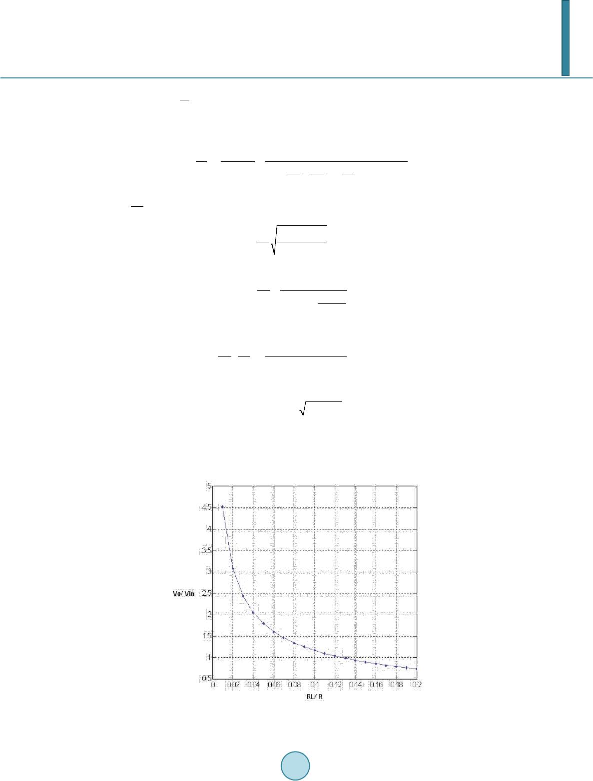 C. A. L. Espinosa /(1) // (1)/1 /0 LL Lin oo ii RLD LDL dV VV D CRC dt − −− = + −− (7) Using Laplace to solve this first order equation, the voltage inp ut -to-o utp ut transfer function is, ( )( ) ( ) () 2 2 11 11 1 o vin DD V Gs R VLC s sD RC LLC − == ∝ +++− +∝ (8) where The corner frequency is (9) In steady state, the transfer function is, () () 11 o VDC in VD MV DD = =∝ −+ − (10) Maximum gain occurs when, ( ) ( ) ( ) 2 2 2 12 0 1 o in DD V DV D −− ∝+∝ ∂= = ∂ − +∝ (11) That is, (12) Figure 2 shows the maximum gain of the circuit for values of α between 0.01 and 0.2. As seen, lower values of α give bigger values of gain and the circuit gets closer to an ideal circuit. Considering this, buc k-boost DC to DC converter operates in continuous conduction mode it is necessary to make sure the lowest inductor current is above cero: Figure 2. Voltage gain vs. RL/R of a buck-boost converter.  C. A. L. Espinosa (13) If this condition is not considered, the inductor current will have times with zero current and the circuit will work in non continuous mode. Here , the peak currents of the inductor, and is the average inductor current. The average inductor current is, (14) When switch is open, (15) The n, (16) The input current is, (17) From this equation, the DC current transfer function is, (18) Efficiency is calculated from the equation: ( ) 2 1 11 oo VDC IDC in in VI MM VI D ηα = == +− (19) For validating these equations a circuit with some practical characteristics is designed and simulated. This circuit is a 1000 watts buc k -boost DC to DC converter with an input voltage Vin = 170 volts, output voltage Vo = 230 volts, frequency f = 50 kHz and 5% of voltage ripple. α can go up to 0.09, as seen on Figure 2. Working with α = 0.05, (20) With this equation duty cycle could be 0.6594 or 0.9156. As the Figure 3 shows, small parasitic resistance in inductance produces more voltage gain, but a maximum voltage gain does not mean a maximum efficiency. So, in order to have a good efficiency-gain relationship, it is better to work in values of D before the maximum peak of gain, that is, in the left side of the curve. Also, as seen on Vo/Vin, the voltage gain curve has less slope with D between zero and D on the maximum gain than in the rest of the curve, which means that a significant change in voltage gain occurs with D varying between D at the maximum gain and one, where the system becomes un- stable or more difficult to control. In the same Figure 3, it is shown the efficiency of the circuit which achieves around 70% for D = 0.6594 and close to 10% with D = 0.9156. The values of resistances are R = 52.9 for the load and of the per- mitted parasitic resistance of the inductor, so that, (21) To calculate the capacitor, an equation derived from an ideal circuit analysis, most seen on any power elec- tronics books, can be used, since parasitic resistance of the inductor does not interfere with the ripple voltage at the output of the circuit. (22) 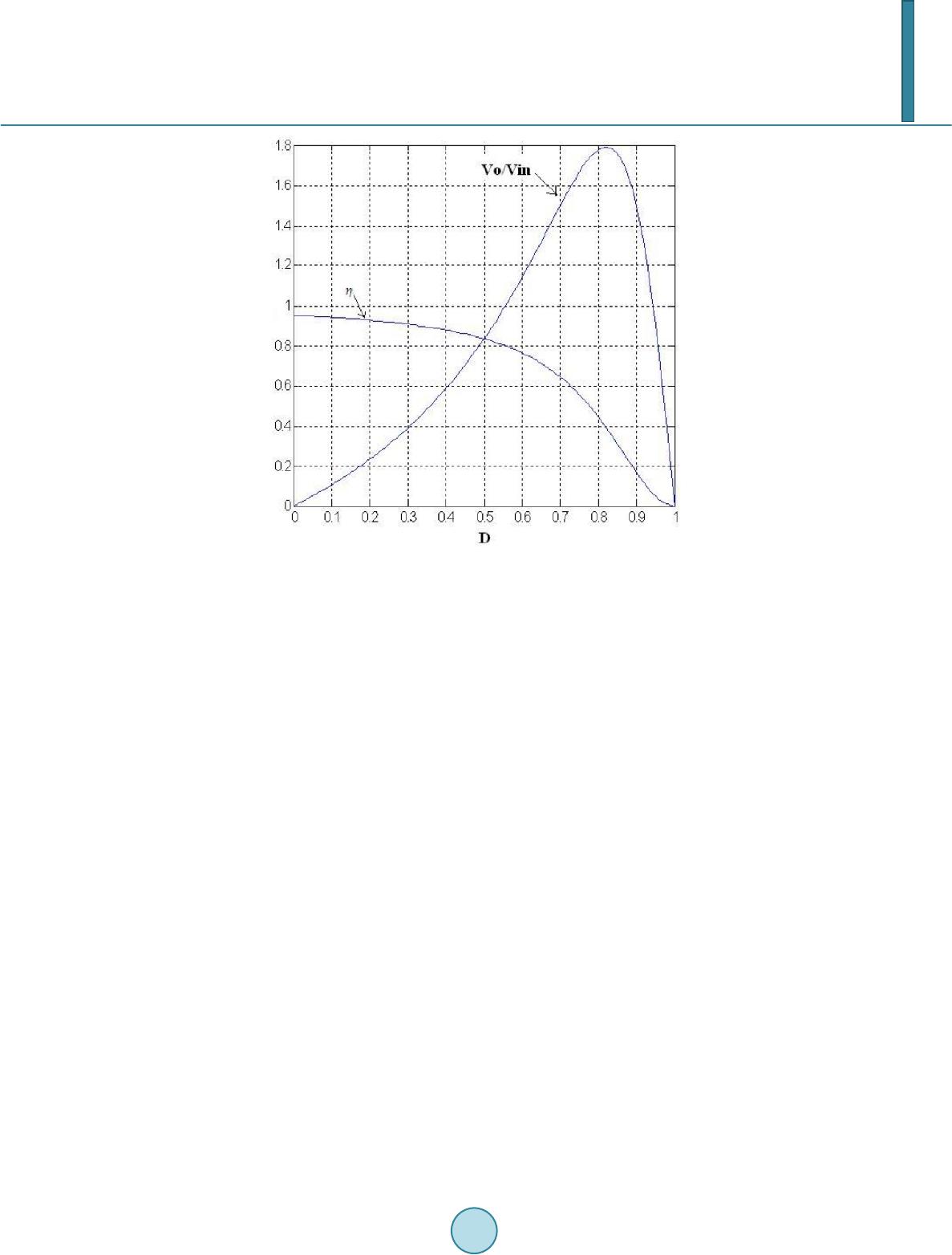 C. A. L. Espinosa Figure 3. Efficiency and voltage gain of a non-ideal bu ck-boost co n- verter with α = 0.05. Simulation of the circuit, using PSIM, is shown in Figure 4 (with the ripple output voltage). In the same Fig- ure 4, it is shown a simulation in Matlab of the step response of the transfer function of the circuit (continuous line). Both simulations curves are superimposed to demonstrate the same response and the validation of the equ- ations with respect to simulations. Small values of parasitic resistances for the inductor will have faster responses but with some overshoot, as in the case of an ideal circuit. Also, bigger values of parasitic resistance for the inductor will have more losses so that the efficiency will be lower and the voltage gain will be reduced. Using same procedure, equations for buck and boost converters can be obtained and they are shown in Table 1 and Tab le 2. For the boost converter the curve of voltage gain vs. α is shown in Figure 5. The efficiency for maximum gain voltage for each value of α is 50%. Efficiency is inversely proportional to α, so that in order to have a better efficiency with a reasonable voltage gain, it is necessary to reduce α by increasing the switching frequency or construct the inductance with a thicker wire. Figure 6 shows voltage gain and efficiency of a boost converter for α = 0.01. With a lower value of α higher efficiency can be obtained with higher voltage gain. For this example 90% efficiency can be achieved with a voltage gain of 3 and α = 0.01. When α = 0.05, for a 90% efficiency only it is possible to have a voltage gain of 1.7. Figure 7 shows voltage gain varying duty cycle for different values of α. 3. Conclusions This analysis has concentrated on finding the ac model of DC to DC buc k, boost and buck-boost converters, on- ly taking into account the parasitic resistance of the inductor. This is because in large voltage conversion, vol- tage drop in semiconductor switch and diode can be neglected and the parasitic resistance of the capacitor can be easy reduced by many in parallel. A b uc k-boost DC to DC converter has been designed for verification of the performance of the circuit and comparison between the model and circuit simulation. As shown, the voltage output of the circuit close follow the equation obtained as a model. Also, the implication of the value of the parasitic resistance of the inductor with respect to the value of the load is shown in a curve for maximum gain, maximizing the gain of the circuit with the duty cycle as the variable to be controlled. 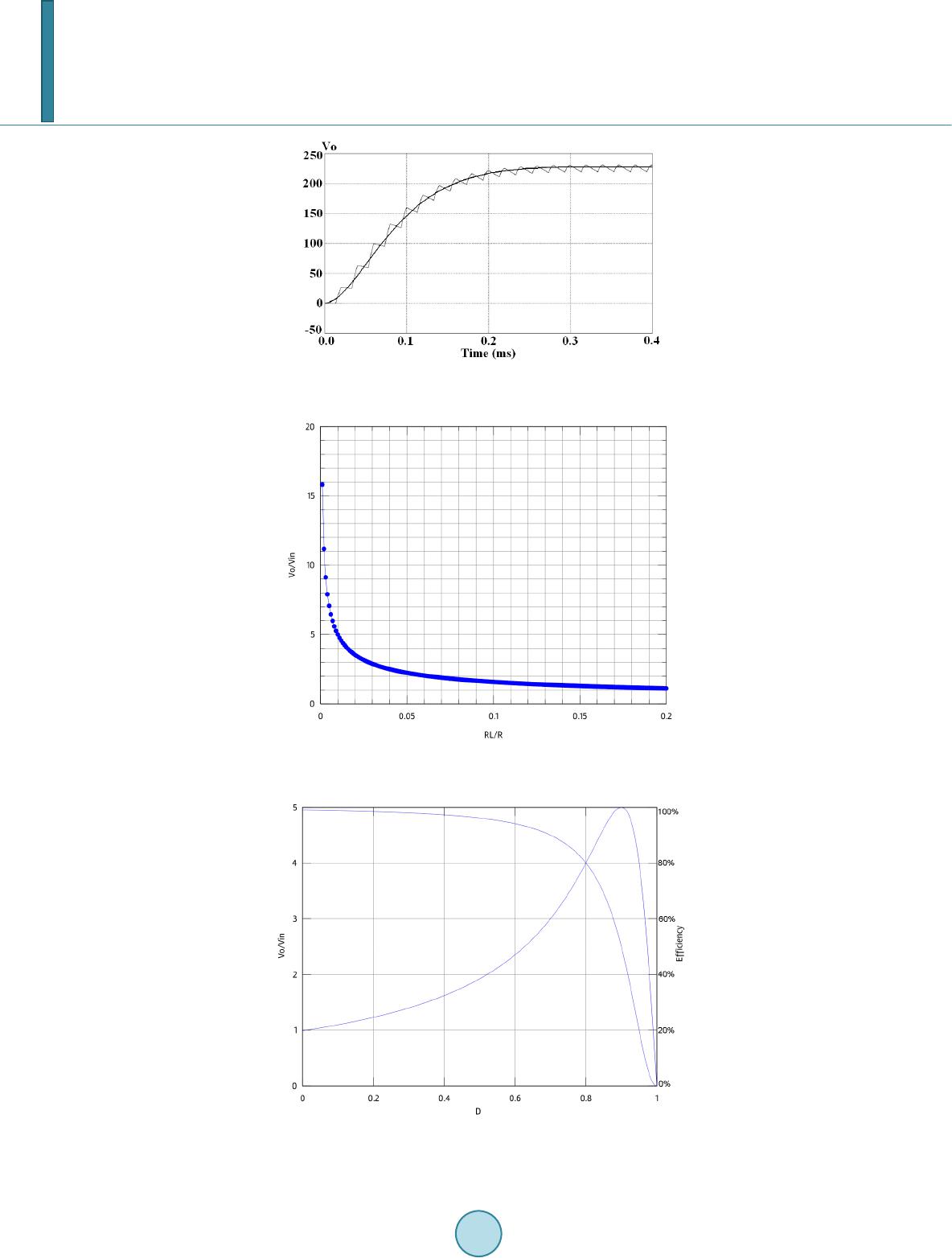 C. A. L. Espinosa Figure 4. Comparison of circuit simulation and step response of transfer function of a non-ideal buc k-boost convert e r. Figure 5. Voltage gain vs. RL/R for boost converters with α be- tween 0.001 and 0.2 . Figure 6. Voltage gain and efficiency for a boost converter with α = 0.01. 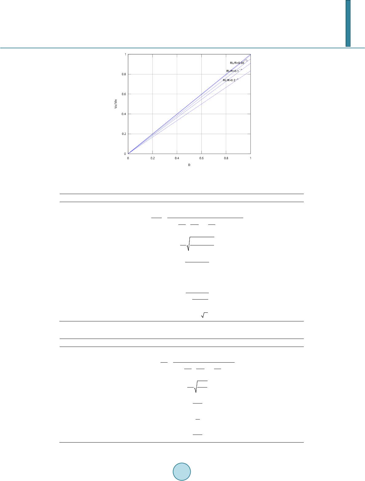 C. A. L. Espinosa Figure 7. Voltage gain vs. duty cycle for a buck converter with α = 0.05, 0.1 and 0.2. Table 1. Small signal model equations for boo st con ve rt er. Boost Converter ( ) ( ) 2 2 11 11 1 D R LC s sD RC LLC − ∝ +++− +∝ Max Gain at Table 2. Small signal model equations for buck convert e r. ( ) 2 1 11 1 D R LC ss RC LLC ∝ ++++∝  C. A. L. Espinosa Equations for buck a nd boost converters are also shown using the same procedure as in buck-boost converter. References [1] Kazimierc zuk, M. and Cravens, R. (1994) Open-Loop DC and Small-Signal Characteristics of PWM Buck-Boost Con- verter for CCM. Aerospace and Electronics Conference, Proceedings of the IEEE, 1, 226-233 . [2] Wang, J.H., Zhang, F.H. and Gong, C.Y. and Chen, R. (2011 ) Modeling and Analysis of a Buck/ Boost Bidirectional Converter with Developed PWM Switch Model. 2011 IEEE 8th International Conference on Power Electronics and ECCE Asia (ICPE & ECCE), May 2011, 705-711 . [3] Neacsu, D., Bonnice, W. and Holmansky, E. (2010) On the Small -Signal Modeling of Parallel/Interleaved Buck/Boost Converters. 2010 IEEE International Symposium on Industrial Electronics (ISIE ), July 2010, 2708 -2713. http://dx.doi.org/10.1109/ISIE.2010.5637070 [4] Wang , Q., Shi L.X. and Chang, C.Y. (2008) Small-Signal Transfer Functions for a Single-Switch Buck-Boost Conver- ter in Continuous Conduction Mode. 2008 ICSICT 9th International Conference on Solid-State and Integrated-Circuit Technology, Beijing, 20-23 October 2008, 2016-2019. [5] Ortiz, C. (2005) Circuit Oriented Average Modeling of Switching Power Converters. 2005 European Conference on Power Electronics and Applications, 1-10. http://dx.doi.org/10.1109/EPE.2005.219694
|

