

Paper Menu >>
Journal Menu >>
 Journal of Modern Physics, 2011, 2, 398-403 doi:10.4236/jmp.2011.25049 Published Online May 2011 (http://www.SciRP.org/journal/jmp) Copyright © 2011 SciRes. JMP Pulsed Supermagnetron Plasma CVD of a-CNx:H Electron-Transport Films for Au/a-CNx:H/p-Si Photovoltaic Cells Haruhisa Kinoshita, Hiroyuki Suzuki Research Institute of Electronics, Shizuoka University, Shizuoka, Japan E-mail: [email protected] Received February 28, 2011; revised April 16, 2011; accepted April 27, 2011 Abstract Hydrogenated amorphous carbon nitride (a-CNx:H) films were formed on p-Si wafers set on a lower elec- trode by pulsed supermagnetron plasma CVD using i-C4H10 and N2 gases. Lower electrode RF power (LORF) of 13.56 MHz (50 - 800 W) was modulated by a 2.5-kHz pulse at a duty ratio of 12.5%, and upper electrode RF power (UPRF) of 50 - 400 W was supplied continuously. The optical band gap decreased with an in- crease in LORF at each UPRF. The open circuit voltage of Au/a-CNx:H/p-Si photovoltaic cells (a-CNx:H film thickness: 25 nm) was about 200 mV for each cell, and the short circuit current density and energy con- version efficiency increased with LORF for each UPRF. The highest energy conversion efficiency of 0.81% was obtained at UPRF/LORF of 200/800 W. Keywords: a-CNx:H film, Supermagnetron Plasma, Pulsed Plasma, CVD, Photovoltaic Cell 1. Introduction Until now, silicon and compound-semiconductor-based materials have dominated the research and market for photovoltaic cells (PVCs). These PVCs utilize p-n junc- tions for the separation of photo-generated carriers. Hy- drogenated amorphous carbon (a-C:H) has been applied in PVCs, as a semiconductor, though the use of these PVCs is still rather limited [1-4]. a-C:H and its nitride (a-CNx:H) showed more than ten orders of magnitude difference in room temperature conductivity, depending on the deposition method used [5-7]. The proportion of sp2 hybridized carbon atoms and their clustering in smaller or larger size determine the optical band gap and produce a significant influence on the electrical transport as well [7-9]. Pulsed discharge of RF plasma is useful to suppress wafer temperature, because the mean RF power supplied to the wafer becomes small because of the pulsing. In the case of pulsed discharge of RF plasma, high pulse-fre- quency is important because the oscillation of wafer temperature can be reduced by its enhancement [10]. In the case of supermagnetron plasma chemical vapor de- osition (CVD) by continuous plasma discharge, the sub- strate set on a room-temperature stage was easily heated to over 100˚C with an increase in RF power [11]. The increase in substrate temperature degraded the character of the a-CNx:H films. By using RF powers modulated by a 2.5-kHz pulse frequency and a duty ratio (defined as the ratio of pulse on-time to total cycle time) of 12.5%, in the case of supermagnetron plasma CVD, the substrate was cooled stably and relatively hard and homogeneous a-CNx:H films were obtained [12]. In this study, we formed a-CNx:H films on p-Si sub- strates and measured the diode I-V characteristics. We report herein the optical properties and PVC properties of a-CNx:H films, including the short circuit current den- sity (ISC), open circuit voltage (VOC), and energy conver- sion efficiency, for fabricated Au/a-CNx:H/p-Si hetero- junction PVCs. 2. Experimental Procedure A pulsed RF supermagnetron plasma CVD apparatus was used for the deposition of a-CNx:H films [12], as shown in Figure 1. The amplitude of one of the two RF power sources with the same RF frequency of 13.56 MHz was modulated using a pulse generator. Continuous and pulsed RF powers were supplied to the upper and lower electrodes with respect to the grounded metal 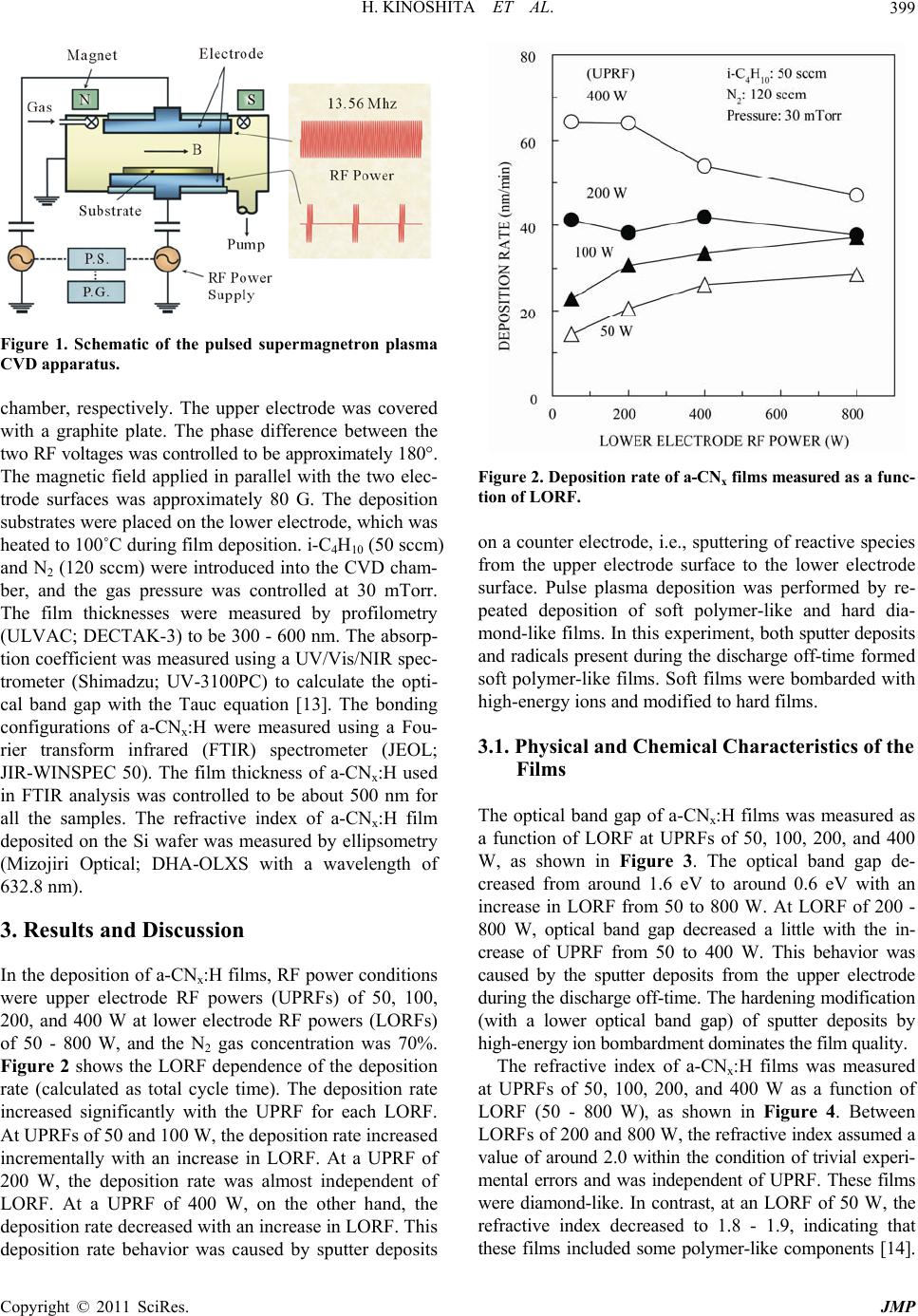 H. KINOSHITA ET AL. Copyright © 2011 SciRes. JMP 399 Figure 1. Schematic of the pulsed supermagnetron plasma CVD apparatus. chamber, respectively. The upper electrode was covered with a graphite plate. The phase difference between the two RF voltages was controlled to be approximately 180°. The magnetic field applied in parallel with the two elec- trode surfaces was approximately 80 G. The deposition substrates were placed on the lower electrode, which was heated to 100˚C during film deposition. i-C4H10 (50 sccm) and N2 (120 sccm) were introduced into the CVD cham- ber, and the gas pressure was controlled at 30 mTorr. The film thicknesses were measured by profilometry (ULVAC; DECTAK-3) to be 300 - 600 nm. The absorp- tion coefficient was measured using a UV/Vis/NIR spec- trometer (Shimadzu; UV-3100PC) to calculate the opti- cal band gap with the Tauc equation [13]. The bonding configurations of a-CNx:H were measured using a Fou- rier transform infrared (FTIR) spectrometer (JEOL; JIR-WINSPEC 50). The film thickness of a-CNx:H used in FTIR analysis was controlled to be about 500 nm for all the samples. The refractive index of a-CNx:H film deposited on the Si wafer was measured by ellipsometry (Mizojiri Optical; DHA-OLXS with a wavelength of 632.8 nm). 3. Results and Discussion In the deposition of a-CNx:H films, RF power conditions were upper electrode RF powers (UPRFs) of 50, 100, 200, and 400 W at lower electrode RF powers (LORFs) of 50 - 800 W, and the N2 gas concentration was 70%. Figure 2 shows the LORF dependence of the deposition rate (calculated as total cycle time). The deposition rate increased significantly with the UPRF for each LORF. At UPRFs of 50 and 100 W, the deposition rate increased incrementally with an increase in LORF. At a UPRF of 200 W, the deposition rate was almost independent of LORF. At a UPRF of 400 W, on the other hand, the deposition rate decreased with an increase in LORF. This deposition rate behavior was caused by sputter deposits Figure 2. Deposition rate of a-CNx films measured as a func- tion of LORF. on a counter electrode, i.e., sputtering of reactive species from the upper electrode surface to the lower electrode surface. Pulse plasma deposition was performed by re- peated deposition of soft polymer-like and hard dia- mond-like films. In this experiment, both sputter deposits and radicals present during the discharge off-time formed soft polymer-like films. Soft films were bombarded with high-energy ions and modified to hard films. 3.1. Physical and Chemical Characteristics of the Films The optical band gap of a-CNx:H films was measured as a function of LORF at UPRFs of 50, 100, 200, and 400 W, as shown in Figure 3. The optical band gap de- creased from around 1.6 eV to around 0.6 eV with an increase in LORF from 50 to 800 W. At LORF of 200 - 800 W, optical band gap decreased a little with the in- crease of UPRF from 50 to 400 W. This behavior was caused by the sputter deposits from the upper electrode during the discharge off-time. The hardening modification (with a lower optical band gap) of sputter deposits by high-energy ion bombardment dominates the film quality. The refractive index of a-CNx:H films was measured at UPRFs of 50, 100, 200, and 400 W as a function of LORF (50 - 800 W), as shown in Figure 4. Between LORFs of 200 and 800 W, the refractive index assumed a value of around 2.0 within the condition of trivial experi- mental errors and was independent of UPRF. These films were diamond-like. In contrast, at an LORF of 50 W, the refractive index decreased to 1.8 - 1.9, indicating that these films included some polymer-like components [14]. 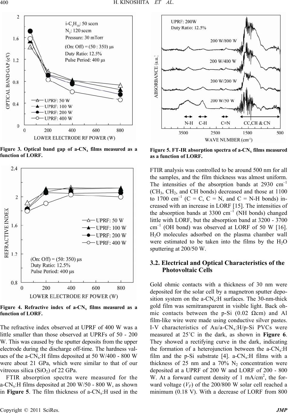 H. KINOSHITA ET AL. Copyright © 2011 SciRes. JMP 400 Figure 3. Optical band gap of a-CNx films measured as a function of LORF. Figure 4. Refractive index of a-CNx films measured as a function of LORF. The refractive index observed at UPRF of 400 W was a little smaller than those observed at UPRFs of 50 - 200 W. This was caused by the sputter deposits from the upper electrode during the discharge off-time. The hardness val- ues of the a-CNx:H films deposited at 50 W/400 - 800 W were about 21 GPa, which were similar to that of our vitreous silica (SiO2) of 22 GPa. FTIR absorption spectra were measured for the a-CNx:H films deposited at 200 W/50 - 800 W, as shown in Figure 5. The film thickness of a-CNx:H used in the Figure 5. FT-IR absorption spectra of a-CNx films measured as a function of LORF. FTIR analysis was controlled to be around 500 nm for all the samples, and the film thickness was almost uniform. The intensities of the absorption bands at 2930 cm–1 (CH3, CH2, and CH bonds) decreased and those at 1100 to 1700 cm–1 (C = C, C = N, and C = N-H bonds) in- creased with an increase in LORF [15]. The intensities of the absorption bands at 3300 cm–1 (NH bonds) changed little with LORF, but the absorption band at 3200 - 3700 cm–1 (OH bond) was observed at LORF of 50 W [16]. H2O molecules adsorbed on the plasma chamber wall were estimated to be taken into the films by the H2O sputtering at 200/50 W. 3.2. Electrical and Optical Characteristics of the Photovoltaic Cells Gold ohmic contacts with a thickness of 30 nm were deposited for the solar cell by a magnetron sputter depo- sition system on the a-CNx:H surfaces. The 30-nm-thick gold film was semitransparent in visible light. Back oh- mic contacts between the p-Si (0.02 Ωcm) and Al film-like wire were made using conductive silver pastes. I-V characteristics of Au/a-CNx:H/p-Si PVCs were measured at 25˚C in the dark, as shown in Figure 6. They showed a rectifying curve in the dark, indicating the formation of a heterojunction between the a-CNx:H film and the p-Si substrate [4]. a-CNx:H films with a thickness of 25 nm and a 70% N2 concentration were deposited at a UPRF of 200 W and LORF of 200 - 800 W. At a forward current density of 1 mA/cm2, the for- ward voltage (VF) of the 200/800 W solar cell reached a minimum (0.18 V). With a decrease of LORF from 800 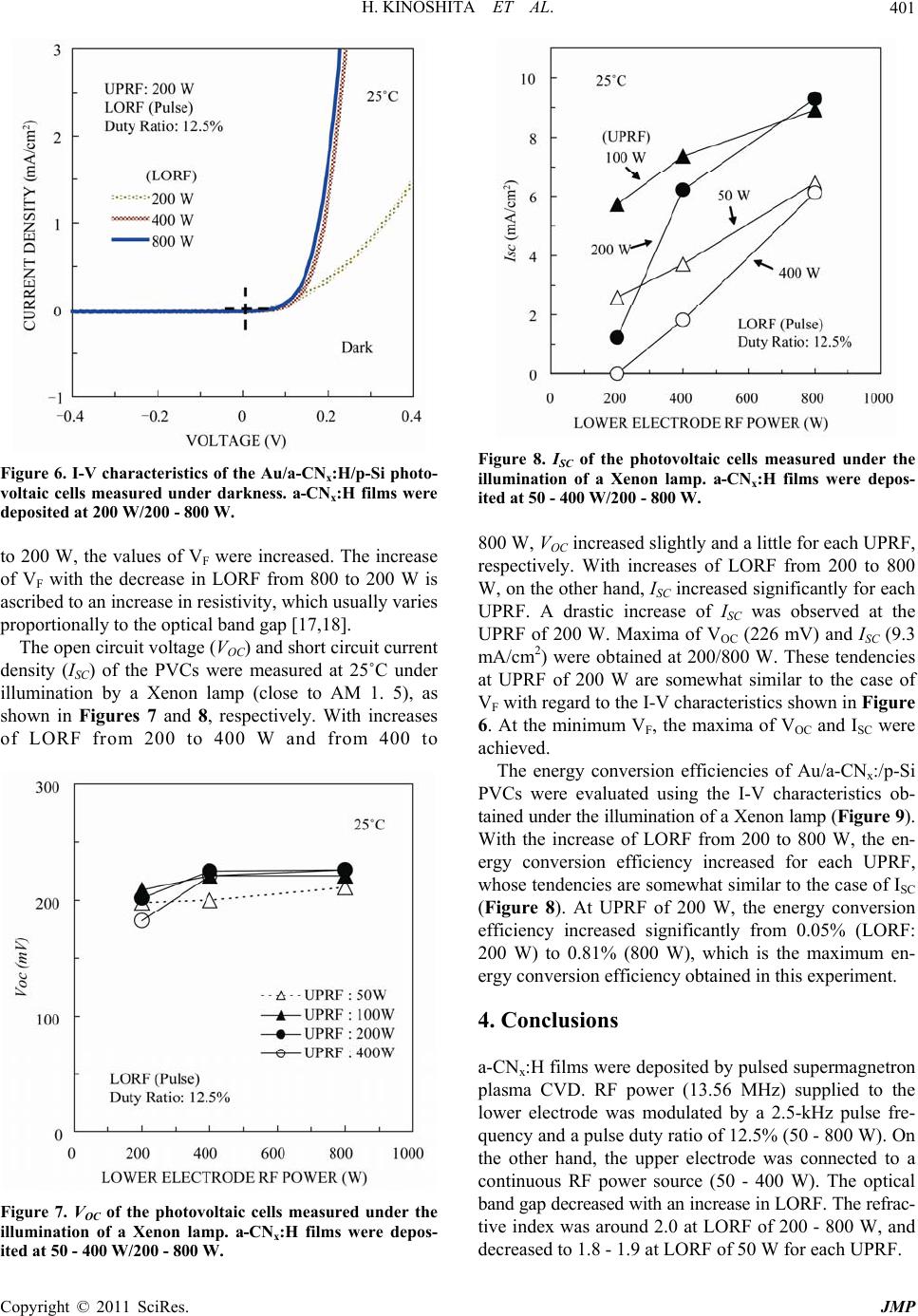 H. KINOSHITA ET AL. Copyright © 2011 SciRes. JMP 401 Figure 6. I-V characteristics of the Au/a-CNx:H/p-Si photo- voltaic cells measured under darkness. a-CNx:H films were deposited at 200 W/200 - 800 W. to 200 W, the values of VF were increased. The increase of VF with the decrease in LORF from 800 to 200 W is ascribed to an increase in resistivity, which usually varies proportionally to the optical band gap [17,18]. The open circuit voltage (VOC) and short circuit current density (ISC) of the PVCs were measured at 25˚C under illumination by a Xenon lamp (close to AM 1. 5), as shown in Figures 7 and 8, respectively. With increases of LORF from 200 to 400 W and from 400 to Figure 7. VOC of the photovoltaic cells measured under the illumination of a Xenon lamp. a-CNx:H films were depos- it ed at 5 0 - 400 W/200 - 800 W. Figure 8. ISC of the photovoltaic cells measured under the illumination of a Xenon lamp. a-CNx:H films were depos- it ed at 5 0 - 400 W/200 - 800 W. 800 W, VOC increased slightly and a little for each UPRF, respectively. With increases of LORF from 200 to 800 W, on the other hand, ISC increased significantly for each UPRF. A drastic increase of ISC was observed at the UPRF of 200 W. Maxima of VOC (226 mV) and ISC (9.3 mA/cm2) were obtained at 200/800 W. These tendencies at UPRF of 200 W are somewhat similar to the case of VF with regard to the I-V characteristics shown in Figure 6. At the minimum VF, the maxima of VOC and ISC were achieved. The energy conversion efficiencies of Au/a-CNx:/p-Si PVCs were evaluated using the I-V characteristics ob- tained under the illumination of a Xenon lamp (Figure 9). With the increase of LORF from 200 to 800 W, the en- ergy conversion efficiency increased for each UPRF, whose tendencies are somewhat similar to the case of ISC (Figure 8). At UPRF of 200 W, the energy conversion efficiency increased significantly from 0.05% (LORF: 200 W) to 0.81% (800 W), which is the maximum en- ergy conversion efficiency obtained in this experiment. 4. Conclusions a-CNx:H films were deposited by pulsed supermagnetron plasma CVD. RF power (13.56 MHz) supplied to the lower electrode was modulated by a 2.5-kHz pulse fre- quency and a pulse duty ratio of 12.5% (50 - 800 W). On the other hand, the upper electrode was connected to a continuous RF power source (50 - 400 W). The optical band gap decreased with an increase in LORF. The refrac- tive index was around 2.0 at LORF of 200 - 800 W, and decreased to 1.8 - 1.9 at LORF of 50 W for each UPRF. 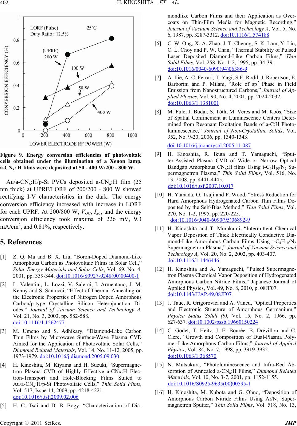 H. KINOSHITA ET AL. Copyright © 2011 SciRes. JMP 402 Figure 9. Energy conversion efficiencies of photovoltaic cells obtained under the illumination of a Xenon lamp. a-CN x: H film s were d eposited at 50 - 400 W/ 200 - 800 W. Au/a-CNx:H/p-Si PVCs deposited a-CNx:H film (25 nm thick) at UPRF/LORF of 200/200 - 800 W showed rectifying I-V characteristics in the dark. The energy conversion efficiency increased with increase in LORF for each UPRF. At 200/800 W, VOC, ISC, and the energy conversion efficiency took maxima of 226 mV, 9.3 mA/cm2, and 0.81%, respectively. 5. References [1] Z. Q. Ma and B. X. Liu, “Boron-Doped Diamond-Like Amorphous Carbon as Photovoltaic Films in Solar Cell,” Solar Energy Materials and Solar Cells, Vol. 69, No. 4, 2001, pp. 339-344. doi:10.1016/S0927-0248(00)00400-1 [2] L. Valentini, L. Lozzi, V. Salerni, I. Armentano, J. M. Kenny and S. Santucci, “Effect of Thermal Annealing on the Electronic Properties of Nitrogen Doped Amorphous Carbon/p-type Crystalline Silicon Heterojunction Di- odes,” Journal of Vacuum Science and Technology A, Vol. 21, No. 3, 2003, pp. 582-588. doi:10.1116/1.1562477 [3] M. Umeno and S. Adhikary, “Diamond-Like Carbon Thin Films by Microwave Surface-Wave Plasma CVD Aimed for the Application of Photovoltaic Solar Cells,” Diamond Related Materials, Vol. 14, No. 11-12, 2005, pp. 1973-1979. doi:10.1016/j.diamond.2005.09.030 [4] H. Kinoshita, M. Kiyama and H. Suzuki, “Supermagne- tron Plasma CVD of Highly Effective a-CNx:H Elec- tron-Transport and Hole-Blocking Films Suited to Au/a-CNx:H/p-Si Photovoltaic Cells,” Thin Solid Films, Vol. 517, Issue 14, 2009, pp. 4218-4221. doi:10.1016/j.tsf.2009.02.006 [5] H. C. Tsai and D. B. Bogy, “Characterization of Dia- mondlike Carbon Films and their Application as Over- coats on Thin-Film Media for Magnetic Recording,” Journal of Vacuum Science and Technology A, Vol. 5, No. 6, 1987, pp. 3287-3312. doi:10.1116/1.574188 [6] C. W. Ong, X.-A. Zhao, J. T. Cheung, S. K. Lam, Y. Liu, C. L. Choy and P. W. Chan, “Thermal Stability of Pulsed Laser Deposited Diamond-Like Carbon Films,” Thin Solid Films, Vol. 258, No. 1-2, 1995, pp. 34-39. doi:10.1016/0040-6090(94)06386-9 [7] A. Ilie, A. C. Ferrari, T. Yagi, S.E. Rodil, J. Robertson, E. Barborini and P. Milani, “Role of sp2 Phase in Field Emission from Nanostructured Carbons,” Journal of Ap- plied Physics, Vol. 90, No. 4, 2001, pp. 2024-2032. doi:10.1063/1.1381001 [8] M. Füle, J. Budai, S. Tóth, M. Veres and M. Koós, “Size of Spatial Confinement at Luminescence Centers Deter- mined from Resonant Excitation Bands of a-C:H Photo- luminescence,” Journal of Non-Crystalline Solids, Vol. 352, No. 9-20, 2006, pp. 1340-1343. doi:10.1016/j.jnoncrysol.2005.11.087 [9] H. Kinoshita, R. Ikuta and T. Yamaguchi, “Sput- ter-Assisted Plasma CVD of Wide or Narrow Optical Bandgap Amorphous CNx:H films Using i-C4H10/N2 Su- permagnetron Plasma,” Thin Solid Films, Vol. 516, No. 13, 2008, pp. 4441-4445. doi:10.1016/j.tsf.2007.10.017 [10] H. Yamada, O. Tsuji and P. Wood, “Stress Reduction for Hard Amorphous Hydrogenated Carbon Thin Films De- posited by the Self-Bias Method,” Thin Solid Films, Vol. 270, No. 1-2, 1995, pp. 220-225. doi:10.1016/0040-6090(95)06892-9 [11] H. Kinoshita and T. Murakami, “Intermittent Chemical Vapor Deposition of Thick Electrically Conductive Dia- mond-Like Amorphous Carbon Films Using i-C4H10/N2 Supermagnetron Plasma,” Journal of Vacuum Science and Technology A, Vol. 20, No. 2, 2002, pp. 403-407. doi:10.1116/1.1446446 [12] H. Kinoshita and A. Yamaguchi, “Pulsed Supermagne- tron Plasma Chemical Vapor Deposition of Hydrogenated Amorphous Carbon Nitride Films,” Japanese Journal of Applied Physics, Vol. 49, No. 8, 2010, p. 08JF07. doi:10.1143/JJAP.49.08JF07 [13] J. Tauc, R. Grigorovici and A. Vancu, “Optical Properties and Electronic Structure of Amorphous Germanium,” Physica Status Solidi (b), Vol. 15, No. 2, 1966, pp. 627-637. doi:10.1002/pssb.19660150224 [14] C. Godet, T. Heitz, J. E. Bourée, B. Drévillon and C. Clerc, “Growth and Composition of Dual-Plasma Poly- mer-Like Amorphous Carbon Films,” Journal of Applied Physics, Vol. 84, No. 7, 1998, pp. 3919-3932. doi:10.1063/1.368570 [15] N. Mutsukura, “Photoluminescence and Infra-Red Ab- sorption of Annealed a-CNx:H Films,” Diamond Related Materials, Vol. 10, No. 3-7, 2001, pp. 1152-1155. doi:10.1016/S0925-9635(00)00595-1 [16] H. Kinoshita, M. Kubota and G. Ohno, “Deposition of Amorphous Carbon Nitride Films Using Ar/N2 Super- magnetron Sputter,” Thin Solid Films, Vol. 518, No. 13,  H. KINOSHITA ET AL. Copyright © 2011 SciRes. JMP 403 2010, pp. 3502-3505. doi:10.1016/j.tsf.2009.11.051 [17] D. I. Jones and A. D. Stewart, “Properties of Hydrogen- ated Amorphous Carbon Films and the Effects of Dop- ing,” Philosophical Magazine B, Vol. 46, No. 5, 1982, pp. 423-434. doi:10.1080/01418638208224021 [18] H. Kinoshita and N. Otaka, “Physical Properties of Ni- trogen-Doped Diamond-Like Amorphous Carbon Films Deposited by Supermagnetron Plasma CVD,” Journal of Vacuum Science and Technology A, Vol. 20, No. 4, 2002, pp. 1481-1485. doi:10.1116/1.1488946 |