

Paper Menu >>
Journal Menu >>
 Journal of Modern Physics, 2011, 2, 248-255 doi:10.4236/jmp.2011.24034 Published Online April 2011 (http://www.SciRP.org/journal/jmp) Copyright © 2011 SciRes. JMP Optical Properties of Aligned Nematic Liquid Crystals in Electric Field Suleyman Yilmaz1, Halide Melik1, Firat Angay1, Mehriban Emek2, Ahmet Yildirim3 1Department of Physics, Harran University, Osmanbey Camp us , Sanliurfa, Turkey 2Department of Physics, Adiyaman University, Adiyaman, Turkey 3Department of Physics, Siirt University, Siirt, Turkey E-mail: [email protected] Received January 13, 2011; revised February 23, 2011; accepted F ebruary 25, 2011 Abstract In this study, the optical transmittance of aligned nematic liquid crystals (ANLCs) was investigated in terms of temperature variations through electrooptic effects under DC electric field. The optical transmittances of the planar and homeotropically aligned liquid crystal cells, which were prepared by conventional rubbing and photolithographic technique on the polyimide thin films for molecular alignment, were measured in their phase transition region. The results of measurement for both orientations, the distribution curve of the optical transmittance exhibits displacement toward to low level at the beginning and then to high level by the tem- perature variations, while the electric field increases. It was also observed that the domain structure of the materials were affected considerably by the applied electric field and phase transition region of the aligned structures had broader range than by the pure crystalline structure and its phase transition temperature was changed by the molecular anisotropy. Finally, in photolithographic method strong bonds between the mole- cules and the orienting surface were observed in high contrast to rubbing method. Keywords: Liquid Crystals, Thin Films, Photolithography, Optical Properties 1. Introduction The nature of the liquid crystals (LC) is very complex and their aligned surface is included the important fac- tors such as van der Waals, dipolar and steric interactions, hydrogen and chemical bonding and surface topography. Their electrooptical properties also play important role on optical processing systems and photonic devices such as mobile phones, smart cards, integrated displays [1,2]. At the same time, NLCs are preferred in many different applications due to their anisotropic structure, which relates to molecular orientation and temperature variation [3-7]. The treatise on the surface of glass substrate constrains the LC and orients the surface director. The characteristic small area and multi domain properties concerned with molecular interactions and the other factors as well as the molecular anisotropy, the electrooptical effects, the an- choring energy, response time, contrast ratio etc. There are several techniques for surface alignment for LCs that depending on contact and non-contact proce- dure. The rubbed polymer technique is widely used in LCDs and the perfect electrooptic performance is pro- vided by this method. However, the fiber residues, the corresponding impurities, the static charges and the me- chanical damage can also trouble for devices and result in deterioration of the quality of LC switching, particu- larly when active matrix elements are used for the pur- pose [8]. Other alignment methods, such as photo- align- ment, micron rubbing by microsphere, nanoim- printing lithography, microcontact printing and ion beam bom- bardment have also intensively studied. In this study, the photolithography method was used to providing the micropatterns on the polyimide surface that includes the spin-coating, the UV exposure and the wet chemical etching, respectively. By taking into account the mentioned properties of NLCs, the optical and the electrooptical properties of randomly [9] and aligned NLCs are examined in the temperature range including phase transitions. 2. Photolithographic Application In these study, commercial NLCs 5CB was provided 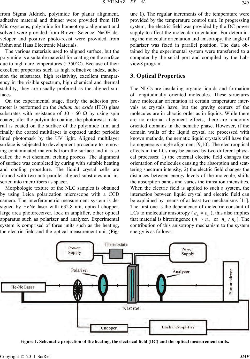 S. YILMAZ ET AL. 249 from Sigma Aldrich, polyimide for planar alignment, adhesive material and thinner were provided from HD Microsystems, polyimide for homeotropic alignment and solvent were provided from Brewer Science, NaOH de- veloper and positive photo-resist were provided from Rohm and Haas Electronic Materials. The various materials used to aligned surface, but the polyimide is a suitable material for coating on the surface due to high cure temperatures (~350˚C). Because of their excellent properties such as high refractive index, adhe- sion the substrates, high resistivity, excellent transpar- ency in the visible spectrum, high chemical and thermal stability, they are usually preferred as the aligned sur- faces. On the experimental stage, firstly the adhesion pro- moter is performed on the indium tin oxide (ITO) glass substrates with resistance of 30 - 60 by using spin coater, after the polyimide coating, the photoresist mate- rial is coated on the surface of the polyimide film and finally the coated multilayer is exposed under periodic lined photomask by the UV light. Aligned multilayer surface is subjected to development procedure to remov- ing contaminated materials from the surface and it is so called the wet chemical etching process. The alignment of surface was completed by curing with suitable heating and cooling procedure. The liquid crystal cells are formed with two anti-parallel aligned substrates and in- serted into microfibers as spacer. Morphologic texture of the NLC samples is obtained by using Leica polarization microscope with a CCD camera. The interferometric measurement system is de- signed by HeNe laser with 632.8 nm, optical chopper, large area photoreceiver, lock in amplifier, other optical apparatus such as polarizer and analyzer. Experimental system is comprised of three units such as the heating, the electric field and the optical measurement unit (Fig- ure 1). The regular increments of the temperature were provided by the temperature control unit. In progressing system, the electric field was provided by the DC power supply to affect the molecular orientation. For determin- ing the molecular orientation and anisotropy, the angle of polarizer was fixed in parallel position. The data ob- tained by the experimental system were transferred to a computer by the serial port and compiled by the Lab- view8 program. 3. Optical Properties The NLCs are insulating organic liquids and formation of longitudinally oriented molecules. These structures have molecular orientation at certain temperature inter- vals as crystals have, but the gravity centers of the molecules are in chaotic order as in liquids. While there are no external alignment effects, there are randomly oriented domains in the nematic phase. However, if the domain walls of the liquid crystal are processed with known methods, the nematic liqu id crystals will have the homogeneous single alignment [9,10]. The electrooptical effects in the LCs may be caused by two different physi- cal processes: 1) the external electric field changes the orientation of molecules causin g the absorption and scat- tering spectrum intensity, 2) the electric field changes the distances between energy levels of the molecule, shifts the absorption bands and varies the transition intensities. When the electric field is applied to such a system, the interaction between liquid crystal and electric field can be explained by means of at least two mechanisms [11]. The first one is the dependency of dielectric constant of LCs to molecular anisotropy (// nn ), this also implies that material is birefringence (// or oe nn ). The contribution of this anisotropy mechanism to the system energy is as follows: Figure 1. Schematic projection of the heating, the electrical field (DC) and the optical measurement units. Copyright © 2011 SciRes. JMP  S. YILMAZ ET AL. Copyright © 2011 SciRes. JMP 250 2 1 8π ea W nE (1) where, n is the director, E is the applied electric field and //a dielectric anisotropy, // and denote parallel to and perpendicu lar constants, respectively. The second mechanism is similar to piezo-electric mecha- nism in solid materials, which small deformations cause formation of polarization. For a weak electric field, the mechanical tension forces are dominant and the orienta- tion of molecular director remains the same. However, the orientation of director starts changing as the applied electric field rises over the critical value (C E ), which is known as Frederick’s transition. To explain this process better, a function known as the coherence length for electric field is used; 12 4π1 a K E E (2) where, denotes the coherence length that ex- presses the distance at which the director vector starts getting affected by the electric field. Here, E K is a con- stant denoting the mechanical tension. Thus, the critical electric field (C E ) is as follows: 12 14π Ca K d E (3) As seen from (Equation (3)), the critical electric field depends on anisotropy (a ) of the material and the thick- ness of the sample (d). The transmittance of the liquid crystal cell is calculated as function of the applied elec- tric field in two steps [12]: firstly, the reorientation of the molecular director must be determined in regards to ap- plied electric field variations and secondly, the orienta- tion of molecules affecting the transmittance of the light through the material must be calculated. These calcula- tions are done by solving numerically the continuity equations for LCs [13]. Thus, anisotropy of molecular structure and the interaction of the incident light with the material determine the polarization of the transmitted light. If a polarization rotation is observed in material, one can tell abou t dichroism of the optically active mate- rial. The dichroism occurs in the LCs due to either the optical anisotropy of the molecular structure or the pres- ence of the impurities. The dichroism also refers to any optical device which can split of light into beams with differing wavelengths. When the light passes through the sample, the polari- zation state of the transmitted light is changed by mo- lecular anisotrop y [14]. In order to calculate the intensity of the light passing through a sample, Jones’ vector rep- resentation is used [15]. The field components of the incident light perpendicular to each other are the follow- ing: ˆ cos xx x Atkz E i (4) ˆ cos yy y Atkz Ej (5) The representation of the incident light components with the Jones’ v ector is the following: x y E E E (6) By the interaction of the transmitted light with the material, the components are the following: ˆ cos xx x Atkz E i (7) ˆ cos yy y Atkz Ej (8) The representation of the transmitted light components with the Jones’ vector is the following: x y E E E (9) Therefore, the optical transmittance of the LC cell sys- tem is calculated by the following equation: 2 2 2 2 xy xy EE TEE (10) 4. Results and Discussions The most common applications of NLC are seen in the electrooptic area depending on temperature. The optical transmittance of NLC 5CB is analyzed under DC electric field in terms of temperature variations. The relative transmittance for both the planar and the homeotropic orientation by the voltage values of 0-15 V is measured in the temperature range from 298 K to 328 K in Figures 2-4. The temperature increment of 3 K per minute is em- ployed during the all measurement. The devised LC systems in this study contain not only the conducting cell of the substrate glasses but also the optical attachments such as polarizer and analyzer. The variation of the anisotropy in the material due to the in- teraction between the material and light under the elec- tric field is monitored and new optical modes are derived from these observations. An increase in the transparency of the sample depending on the temperature is clearly seen from the modulation spectrum graphics in Figures 5-7. The modulation spectrum data gives us detailed in- formation about the optical properties of the material, such as the phase transition, the transparency and the molecular anisotropy. 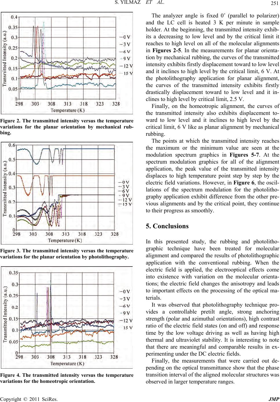 S. YILMAZ ET AL. 251 Figure 2. The transmitted intensity versus the temperature variations for the planar orientation by mechanical rub- bing. Figure 3. The transmitted intensity versus the temperature variations for the planar orientation by photolithography. Figure 4. The transmitted intensity versus the temperature variations for the homeotropic orientation. The analyzer angle is fixed 0˚ (parallel to polarizer) and the LC cell is heated 3 K per minute in sample holder. At the beginning, the transmitted intensity exhib- its a decreasing to low level and by the critical limit it reaches to high level on all of the molecular alignments in Figures 2-5. In the measurements for planar orienta- tion by mechanical rubbing, the curves of the transmitted intensity exhibits firstly displacement toward to low level and it inclines to high level by the critical limit, 6 V. At the photolithography application for planar alignment, the curves of the transmitted intensity exhibits firstly drastically displacement toward to low level and it in- clines to high level by critical limit, 2.5 V. Finally, on the homeotropic alignment, the curves of the transmitted intensity also exhibits displacement to- ward to low level and it inclines to high level by the critical limit, 6 V like as planar alignment by mechanical rubbing. The points at which the transmitted intensity reaches the maximum or the minimum value are seen at the modulation spectrum graphics in Figures 5-7. At the spectrum modulation graphics for all of the alignment application, the peak value of the transmitted intensity displaces to high temperature point step by step by the electric field variations. However, in Figure 6, the oscil- lations of the spectrum modulation for the photolitho- graphy application exhibit difference from the other pre- vious alignments and by the critical point, they continue to their progress as smoothly. 5. Conclusions In this presented study, the rubbing and photolitho- graphic technique have been treated for molecular alignment and compared the results of photolithographic application with the conventional rubbing. When the electric field is applied, the electrooptical effects come into existence with variation on the molecular orienta- tions; the electric field changes the anisotropy and leads to important effects on the processing of the optical ma- terials. It was observed that photolithography technique pro- vides a controllable pretilt angle, strong anchoring strength (polar and azimuthal orientations), high contrast ratio of the electric field states (on and off) and response time by the low voltage driving as well as having high thermal and ultraviolet stability. It is interesting to note that there are meaningful and comparable results in ex- perimenting under the DC electric fields. Finally, the measurements that were carried out de- pending on the optical transmittance show that the phase transition interval of the aligned molecular structures was observed in larger temperature ranges. Copyright © 2011 SciRes. JMP  S. YILMAZ ET AL. Copyright © 2011 SciRes. JMP 252 Figure 5. The modulation spectrum of the optical transmittance versus the temperature variations for the planar orientation by mechanical rubbing.  S. YILMAZ ET AL. 253 Figure 6. The modulation spectrum of the optical transmittance versus the temperature variations for the planar orientation by photolithography. Copyright © 2011 SciRes. JMP  254 S. YILMAZ ET AL. Figure 7. The modulation spectrum of the optical transmittance versus the temperature variations for the homeotropic ori- ntation. e Copyright © 2011 SciRes. JMP  S. YILMAZ ET AL. Copyright © 2011 SciRes. JMP 255 The results of this study, which is accomplished on ran- domly orientated molecules in previous study [16], show resemblance with the results of other works by devel- oped in the past studies [17-24]. 6. Acknowledgements The authors thank to Harran University for financial support. This study is supported by Harran University, the Fund of Scientific Research Projects (SRP) with grant no: 919. 7. References [1] S. Varghese, S. Narayanankutty, C. W. M. Bastiaansen, G. P. Crawford and D. J. Broer, “Patterned Alignment of Liquid Crystals by m-Rubbing,” Advanced Materials, Vol. 16, 2004, pp. 1600-1605. doi:10.1002/adma.200306536 [2] V. A. Konovalov, V. G. Chigrinov, H. S. Kwok, H. Ta- kada and H. Takadsu, “Photoaligned Vertical Aligned Nematic Mode in Liquid Crystals,” Japanise Journal of Applied Physics, Vol. 43, No. 1, 2004, pp. 261-266. doi:10.1143/JJAP.43.261 [3] P. G. de Gennes and J. Prost, “The Physics of Liquid Crystals,” Oxford University Press, UK, 1993. [4] H. Gleeson, “Introduction to Liquid crystals,” Manches- ter University Press, UK, 1998. [5] I. C. Khoo, “Liquid Crystals: Physical Properties and Nonlinear Optical Phenomena,” John Wiley & Sons, Inc., New York, 1995. [6] P. Klysubun, “Nonlinear Optical Studies of Dye-Doped Nematic Liquid Crystals,” PhD Dissertation, Virginia Polytechnic Institute and State University, Virginia, 2002. [7] S. Yilmaz, and A. Bozkurt, “Spectroscopic Measurement of Liquid Crystal Anisotropy in the Ultraviolet/Visible Region,” Materials Chemistry and Physics, Vol. 107, No. 2-3, pp. 410-412. [8] V. G. Chigrinov, “Liquid Crystal Devices: Physics and Applications,” Artech House, Boston, 1999. [9] M. Emek, N. Besli, A. Yildirim and S. Yilmaz, “Optical Properties of Nematic Liquid Crystal (C21H27NO2S) Un- der AC/DC Electric Fiel ds” Canadian Journal of Physics, Vol. 87, No. 4, 2009, pp. 293-298. doi:10.1139/P09-030 [10] P. Yeh, and C. Gu, “Optics of Liquid Crystal Display,” John Wiley & Sons, New York, 1999. [11] S. Kumar, “Liquid Crystals: Experimental Study of Physical Properties and Phase Transitions,” Cambridge University Press, Cambridge, 2001. [12] J. Osterman, L. Madsen, J. Birgerson and K. Skarp, “Op- tical Properties of Single-Polarizer Reflective Bistable Nematic Displays,” SID Symposium Digest of Technical Papers, Vol. 34, 2003, pp. 950-953. doi:10.1889/1.1832441 [13] D. Kang, J. E. Maclennan, N. A. Clark, A. Zakhidov and R. H. Baughman, “Electro-Optic Behavior of Liquid- Crystal-Filled Silica Opal Photonic Crystals: Effect of Liquid-Crystal Alignment,” Physical Review Letters, Vol. 86, No. 18, 2001, pp. 4052-4055. doi:10.1103/PhysRevLett.86.4052 [14] S. Yilmaz, “Light Scattering By Some Nematic Liquid Crystals Due to Phase Transitions,” Journal of Quanta- tive Spectroscopy and Radiative Transfer, Vol. 104, No. 3, 2007, pp. 305-309. doi:10.1016/j.jqsrt.2006.02.002 [15] J. Osterman, “Investigations of Optical Properties and Photo-Alignment in Bistable Nematic Liquid Crystal Displays,” PhD Dissertation, Uppsala University, Sweden, 2005. [16] S. Yilmaz, “Optical Properties of Some Mixed Nematic Liquid Crystals in Electric Field,” Materials Chemistry and Physics, Vol. 110, No. 1, 2008, pp. 140-144. doi:10.1016/j.matchemphys.2008.01.027 [17] Y. Suzuki, N. Mizoshita, K. Hanabusa and T. Kato, “Homeotropically Oriented Nematic Physical Gels for Electrooptical Materials,” Journal of Materials Chemistry, Vol. 13, No. 12, 2003, pp. 2870-2874. doi:10.1039/b308098f [18] R. Bartolino, N. Scaramuzza, D. E. Lucchetta, E. S. Ba- rna, A.Th. Ionescu and L.M. Blinov, “Polarity Sensitive Electrooptical Response in a Nematic Liquid Crystal- Polymer Mixture,” Journal of Applied Physics, Vol. 85, No. 5, 1999, pp. 2870-2874. doi:10.1039/b308098f [19] H. Y. Chen and W. Lee, “Electro-Optical Characteristics of a Twisted Nematic Liquid-Crystal Cell Doped with Carbon Nanotubes in a DC Electric Field,” Optical Re- views, Vol. 12, No. 3, 2005, pp. 223-225. doi:10.1007/s10043-005-0223-7 [20] J. G. Yoo, B. S. Song and J. Kim, “Surface Pretilt Effects of Bistable Twisted Nematic Liquid Crystal Display,” Japanise Journal of Applied Physics, Vol. 38, No. 10, 1999, pp. 6005-6007. doi:10.1143/JJAP.38.6005 [21] H. L. Margaryan and V. M. Aroutiounian, “Influence of Longitudinal Electric Field on Time Characteristics of Freedericksz Transition,” Moleculer Crystals and Liquid Crystals, Vol. 454, No. 1, 2006, pp. 513-523. [22] J. W. Han, “Effect of the Nematic-Isotropic Phase Tran- sition on the Electro-Optical Characteristics of Polimer- Dispersed Liquid Crystal Films,” Journal of the Korean Physical Society, Vol. 40, No. 5, pp. 849-855. [23] T. Takematsu, H. Okada and H. Onnagawa, “Characteris- tics of Modulated Microdomain Switching Using Nematic Liquid Crystals,” Japanese Journal of Applied Physics, Vol. 41, No. 2A, 2002, pp. 733-736. doi:10.1143/JJAP.41.733 [24] J. Merlin, E. Chao, M. Winkler and K. D. Singer, P. Korneychuk and Y. Reznikov, “All-Optical Switching in a Nematic Liquid Crystal Twist Cell,” Optics Express, Vol. 13, No. 13, 2005, pp. 5024-5029. doi:10.1364/OPEX.13.005024 |