

Paper Menu >>
Journal Menu >>
 Journal of Power and Energy Engineering, 2014, 2, 477-482 Published Online April 2014 in SciRes. http://www.scirp.org/journal/jpee http://dx.doi.org/10.4236/jpee.2014.24064 How to cite this paper: Du, L.J., et al. (2014) An Ultra-Low Quiescent Current CMOS Low-Dropout Regulator with Small Output Voltage Va riations. Journal of Power and Energy Engineering, 2, 477-482. http://dx.doi.org/10.4236/jpee.2014.24064 An Ultra-Low Quiescent Current CMOS Low-Dropout Regulator with Small Output Voltage Variations Longjie Du1, Yizhong Yang1, Yang Chen1, Guangjun Xie1,2, Xin Cheng1,2* 1School of Electronic Science and Applied Physics, Hefei University of Technology, Hefei, China 2State Key Lab of ASIC and System, Fudan University, Shanghai, China Email: *[email protected] Received Dec emb er 2013 Abstract An ultra-low quiescent current low-dropout regulator with small output voltage variations and improved load regulation is presented in this paper. It makes use of dynamically-biased shunt feedback as the buffer stage and the LDO regulator can be stable for all load conditions. The pro- posed structure also employs a momentarily current-boosting circuit to reduce the output voltage to the normal value when output is switched from full load to no load. The whole circuit is de- signed in a 0.18 μm CMOS technology with a quiescent current of 550 nA. The maximum out- put-voltage variation is less than 20 mV when used with 1 μF external capacitor. Keywords Ultra-Low Quiescent Current; Low-Dropout Regul ato r; Small Output Vari ati ons 1. Introduction Power-management circuits are becoming more important in portable electronics systems such as smart phones, laptops, and tablets. The performance of these portable devices is increasing fast and the battery life is becoming the bottleneck for their development. So it is in great demand to design the power-management circuits with ul- tra-low power dissipation and a wide output current range. For power-management system, low-dropout regulator is the most common block due to better load transient response, less noise, simpler and lower cost than the switching regulator counterparts [1]-[3]. However, when it comes to design an ultra-low quiescent current LDO, it is difficult to satisfy these characteristics. In a co nve n- tional low-dropout regulator, there are several specifications to describe the LDO’s performance, such as line and load regulations, loop stability and transient response. When the whole LDO’s quiescent current is low, the loop stability and transient response are sacrificed a lot due to the low frequency pole at the error amplifier out- put, the decreased loop bandwidth and the limited slew rate at the gate of power transistor. Furthermore, the de- mand of a large maximum load-current also affects the loop stability and transient response because it introduc- * Corresponding author. 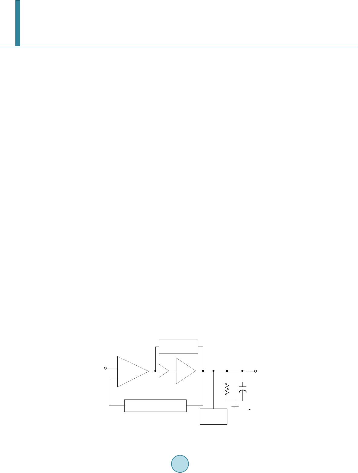 L. J. Du et al. 478 es a large capacitor at the gate of power transistor. The large capacitor will reduce the value of the parasitic pole present at the gate of the power transistor and require more sourcing and sinking currents at the gate to maintain the slew rate. Therefore, there are two main challenges in the ultra-low quiescent current design. One is the fre- quency compensation strategy for the stability under whole load-current range, and the other is how to achieve good transient response [4]. Different approaches have been reported to address the above issues. For frequency compensation, the con- ventional method is making use of the equivalent series resistance (ESR) of the output capacitor to create a con- stant zero for compensating the non-dominant pole [5] [7]-[9]. However, it may not be fit for LDO with wide load current requirement, because the frequency of the output pole will change a lot when the load current varies. In [1], an emitter-follower with small output resistance has been adopted to push the pole at the gate of the pow- er device beyond the unity-gain frequency of the LDO loop. However, when the LDO is used to source a larger load current, more current are needed in its emitter-follower. Thus the resistance at the gate of the power tran- sistor can be further lowered to compensate the larger gate capacitance. Further architecture is used in [3] [6] to push the pole at the gate of the power transistor to a higher frequency. Both of the loop-gain bandwidth and the slew rate at the gate of the power transistor dominate the transient response of a LDO. There are typically two methods to raise the slew rate at the gate of the power transistor. One is using a smaller area power transistor [10], and the other is providing more sourcing and sinking currents at the gate capacitor. Many design approaches have been proposed to realize the current boosting at the gate of power transistor they can be classified into three techniques depending on the changing time of the biasing cur- rent. In [11], the biasing current is always high and independent of the load current. Obviously, this approach is not suit for low quiescent current design for the high biasing current at light load. Consequently, the adap- tive-biasing technique which can increase the bias current according to the magnitude of the output current is proposed in [1] [3] [6]. To further reduce power dissipation in the steady state, dynamic biasing which only in- creases the biasing current at the transient instant when the output current is changed is presented [4] [5] [12]. This paper presents an ultra-low quiescent LDO regulator using an adaptive-biasing voltage buffer and an overshoot reduction network in 0.18 μm CMOS process. Section 2 discusses the structure as well as the stability of the proposed LDO regulator. In Section 3, the details of the circuit implementation of the proposed structure are described. Simulation results and conclusions are given in the last two sections. 2. Structure of the Proposed LDO Figure 1 shows the proposed LDO regulator architecture. It comprised a folded-cascode error amplifier, an adaptive biasing voltage buffer, a power transistor MP, an overshoot reduction circuitry, a frequency compensa- tion network and a feedback network. The adaptive-biasing voltage buffer is employed for isolating the large parasitic capacitance at the gate of MP from the high impedance at the error amplifier output. It is also used for the slew rate enhancement. In addition, the overshoot reduction network can decrease the output voltage down to the normal value at no load condition. Thanks to the low out impedance of the voltage buffer, the pole at the gate of power transistor is located at sufficiently high frequencies under different load currents. Figure 1. Structure of the proposed LDO regulator. - + Frequency Compensation Feedback Network Overshoot Reduction RO Error Amp Vref CL MP Vout Buffer 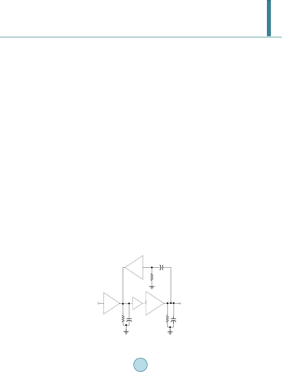 L. J. Du et al. 479 The stability of the whole system is achieved by cascode compensation technique, which allows the LDO to achieve wider unity gain frequency and enhanced power supply rejection [3]. The sma ll-signal model of the pro- posed LDO is shown in Figur e 2. Here, gm1 and gmp represent the transconductances of input gain stage of error amplifier and power transistor respectively, R1 is the output resistance of the error amplifier, C1 is the input ca- pacitance of the buffer stage, CL is the output capacitance, and RO is the equivalent resistance seen at the output of the LDO. The cascode compensation is formed by gmc and CC and only takes effect at heavy load. So at light load, the pole located at the output of the LDO is the dominant pole, and the pole located at the output of the er- ror amplifier is the non-dominant pole. They are given by 3 11 1/( ) dB p RC − = (1) 1/( ) ndO O p RC= (2) When the output load is heavy, the impedance at the output of LDO becomes small while the capacitor at the output or the error amplifier becomes large because of the enhancement of a Miller capacitance (gmpRO) CC. So the above two poles will shift their positions at heavy load. The worst-case stability resides between light load and heavy load [6]. 3. Circuit Design and Implementation The full schematic of the proposed LDO is shown in Fig ure 3. The error amplifier is realized by a single folded- cascode stage with transistors M0-M8. The voltage buffer is formed by a source-follower M12. And the transistor M14 is the feedback device connected in parallel to the output of M12 in order to reduce the output impedance. The adaptive biasing network is formed by transistor M15 and M16, which is used for both compensation and slew rate enhancement. The feedback network is realized by a string of diode-connected PMOS transistors M18 - M21 biased in the sub threshold region to minimize quiescent as well as the silicon area. Transistor M6 and capa- citor CC form the cascode compensation to make the LDO be stable under full load range. Finally, the overshoot reduction network is realized by Rb, Cb and transistor M17. In a conventional LDO, when the load current sud- denly decreases to zero, the diode-connected feedback network PMOS is the only path to discharge the extra current from power transistor MP. So, even if the error amplifier reacts quickly to increase the gate voltage of MP, the overshoot appears at the output would still take a very long time to recover to the nominal value. But with the help of overshoot reduction network, when the gate voltage of MP suddenly increases, the change is sensed by Cb and is then coupled to the gate of M17. Hence transistor M17 provides the second path to discharge the overshoot. When the gate voltage of MP becomes steady, the gate voltage of M17 recovers to Vb2 [4]. In steady state, the current flow through M17 is around 100 nA. 4. Simulation Results The proposed ultra-low quiescent LDO regulator was designed and simulated in a 0.18 μm CMOS technology. The input voltage range of the LDO is designed from 1.8 V to 5.5 V and the output voltage is set to 1.6 V. The Figure 2. S mal l-signal modeling of the proposed LDO. +g m1 x1 -g mp +g mc R 1 C 1 R O C L 1/g mc C C V out V in 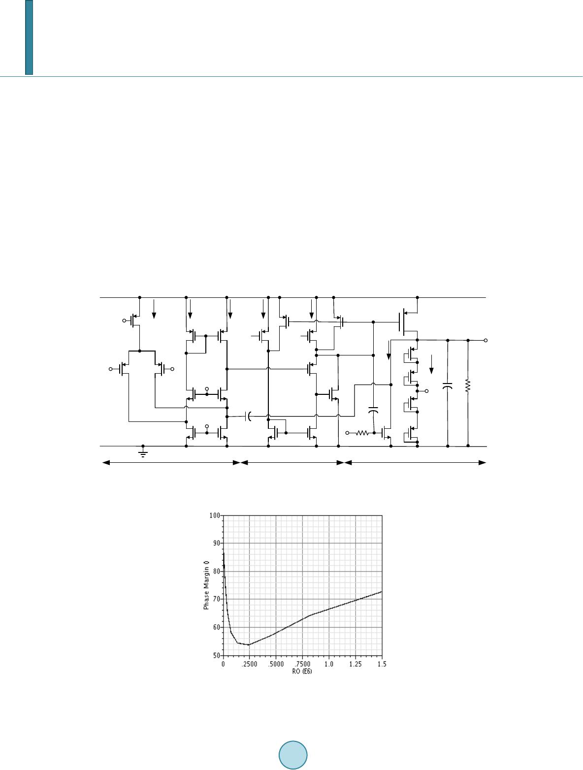 L. J. Du et al. 480 output capacitor is 1 μF. The output current range is from 0 to 100 mA when the dropout voltage is 0.2 V. The LDO consumes an ultra-low quiescent current of 550 nA under no-load condition, while a quiescent current of 135 μA is dissipated at full load condition. The stability of the LDO under different load conditions was verified. Figure 4 shows the simulated phase margin of the loop-gain transfer function under different load currents. The minimum phase margin is always larger than 54˚ for the entire range of load current. Figure 5 shows the transient response of the proposed LDO when the load current is pulsating between 0 and 100mA with pulse rise and fall time of 1 μs. With the use of a 1μF output capacitor, the maximum output vol- tage variation is less than 20 mV when dropout voltage is 0.2 V, which includes output undershoots, overshoots and variations due to load regulation. It can be seen that the output voltage was hardly regulated to the nominal value without overshoot reduction. The line transient response is shown in Figure 6. The supply voltage changes between 1.8 V and 2 V in 10 μs with an output current of 100 mA. The simulated result shows that the total output voltage variations are less than 2 mV. Finally, a comparison of some reported LDOs is given in Table 1. A figure of merit used in [3] is adopted here to compare the transient response of different LDOs. The smaller FOM value, the better is the transient performance metric. The proposed design achieves the smallest FOM value among the recently reported works. Figure 3. Schematic of the proposed LDO regulator. Figure 4. Phase margin of the proposed LDO loop- gain transfer function under different load currents with a 1 μF output capacitor. M 0 M 1 M 2 M 7 M 8 M 5 M 6 M 3 M 4 M 10 M 9 V b4 M 13 V b5 M 16 M 15 M P M 12 M 11 V b2 R 1 M 17 M 18 C 1 M 19 M 20 M 21 C L R O V b1 V fb V ref C C M 14 V fb V b2 V b3 V out V in Fol ded-cascode error amplifierAdaptive biasing voltage bufferPower transistor and overshoot reduction 80nA60nA60nA 50nA100nA 50nA 100nA 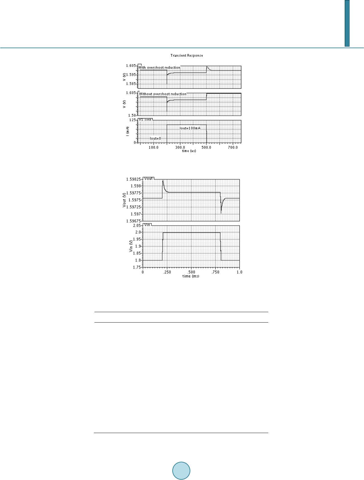 L. J. Du et al. 481 Figure 5. Simulated load transient response of the pro- posed LDO. Figure 6. Simulated line transient response of the pro- posed LDO. Table 1. Performance comparison with previously reported LDOs. [5] 2010 [6] 2011 [8] 2013 [9] 2013 This work Technology (μm) 0.35 0.35 0.18 0.09 0.18 Vin (V) 2 3.3-7 1.8 1 1.8-5 Vout (V) 1.8 3 1.64 0.85 1.6 Imax (mA) 100 100 150 100 100 Iq (μA) 4 0.5 0.33 60 0.55 Vdo (mV) 200 300 160 150 200 Load regulation (mV/mA) N/A 0.15 0.33 0.28 0.03 CL (μF) 1-10 1 13.125 1 1 ΔVout (mV) 55 150 48 28 20 Tr (μs) 0.55 1.5 4.2 0.28 0.2 FOM* (ns) 0.022 0.0075 0.00924 0.168 0.0011 * , max (/ ) rq L FOMT II= .  L. J. Du et al. 482 5. Conclusion In this paper, an ultra-low quiescent current low dropout regulator based on an adaptive-biasing voltage buffer and an overshoot reduction network has been presented. The adaptive-biasing voltage buffer is employed both for frequency compensation and slew rate enhancement. In addition, an overshoot reduction net-work is used to regulate the output voltage back to its normal value when the output is switched from full load to no load. The LDO is able to source up to 100 mA of output current and dissipates only 550 nA quiescent current at no load condition. Acknowledgem ents This paper is supported by Fudan University State Key Laboratory of ASIC & System (12KF001), Fudan Uni- versity State Key Laboratory of ASIC & System Senior Visiting Scholarship (11FG029), Intercollegiate Key Project of Nature Science of Anhui Province (KJ2011A213) and Science and Research Funds of Hefei Univer- sity of Technology (2013HGXJ0192). References [1] Rincon-Mora, G.A. and Allen, P.E. (1998) A Low-Voltage, Low Quiescent Current, Low Drop-out Regulator. IEEE Journal of Solid -State Circuits, 33, 36-44. http://dx.doi.org/10.1109/4.654935 [2] Leung, K. N. and M o k, P.K.T. (2003) A Cap acito r-Free CMOS Low-Dropout Regulator with Damp ing-F actor-Control Frequency Compensation. IEEE Journal of Solid-State Circuits, 38, 1691-1702. http://dx.doi.org/10.1109/JSSC.2003.817256 [3] Al -Sh youkh, M., Lee, H. and Perez, R. (2007) A Transient-Enhanced Low-Quiescent Current Low-Dropout Regulator with Buffer Impedance Attenuation. IEEE Journal of Solid-State Circuits, 42, 1732-1742. http://dx.doi.org/10.1109/JSSC.2007.900281 [4] Or, P.Y. and Leung, K.N. (2010) An Output-Capacitor Less Low-Dropout Regulator with Direct Voltage-Spike Detec- tion. IEEE Journal of Solid-State Circuits, 45, 458-46 6. http://dx.doi.org/10.1109/JSSC.2009.2034805 [5] Leung, K. and Ng, Y.S. (20 10 ) A CMOS Low-Dropout Regulator with a Momentarily Current-Boosting Voltage Buf- fer. IEEE Transactions on Circuits and Systems I: Regular Papers, 57, 2312-2319. [6] Hu, J., Hu, B., F an, Y. and Ismail, M. (2011) A 500 nA Quiescen t, 100 mA Maximum Load CMOS Low-Dropout Regulato r. IEEE International Conference on Electronics, Circuits and Systems, 386-389. [7] Guo, J., Cao, Y. and Lai, X. (20 09) An Inner ESR-Fungible Compensation Technique for Ultra-Low Power Low Drop- out Regulators. Analog Integrated Circuits and Signal Processing, 61, 265-270. http://dx.doi.org/10.1007/s10470-009-9302 -1 [8] Sal ehi, M.R. and Mohammadalinejadi, S. (2013 ) A Low Dropout Voltage Regulator with Enhanced Transconductance Error Amplifier and Small Output Voltage Variations. Pro c eeding of Iranian Electrical Engineering Conference, 1-5. [9] Huang, C.H., Ma, Y.T. and Liao, W.C. (2013) Design of a Low-Voltage Low-Dropout Regulator. IEEE Transactions on Very Large Scale Integration Systems, 99, 1-5. [10] Gutierrez, L., Roa, E. and Hernandez, H. (2009) A Current Efficient, Lo w-Dropout Regulator with Improved Load Regulation. IEEE Workshop on Microelectronics and Electron Devices, 1-4. [11] Hazucha, P., Kar ni k, T., Bradley, B.A., Parsons, C., Finan, D. and Borkar, S. (2005) Area-Efficient Linear Regulator with Ultra-Fast Load Regulation. IEEE Journal of Solid-State Circuits, 40, 933-940. http://dx.doi.org/10.1109/JSSC.2004.842831 [12] Man, T.Y., Mo k, P.K.T. and Chan, M. (2007) A High Slew-Rate Push-Pull Output Amplifier for Low-Quiescent Cur- rent Low-Dropout Regulators with Transi ent-Response Improvement. IEEE Transactions on Circuits and Systems II: Express Briefs, 54, 755-759. |