

Paper Menu >>
Journal Menu >>
 Materials Sciences and Applicatio ns, 2011, 2, 265-269 doi:10.4236/msa.2011.24034 Published Online April 2011 (http://www.scirp.org/journal/msa) Copyright © 2011 SciRes. MSA Low Temperature Gas Sensing Coatings Made through Wet Chemical Deposition of Niobium Doped Titanium Oxide Colloid Naji Al Dahoudi Physics Department, Al Azhar University, Gaza, Palestine. Email: [email protected] Received January 6th, 2011; revised February 28th, 2011; accepted March 17th, 2011. ABSTRACT Niobium doped titanium oxide (TiO2) colloid was synthesized to fabricate a hydrog en gas sensor layer on oxidized sili- con wafer substrate. The layers were obtained using spin coating technique and then heated in air at 500˚C for 30 min. The doping of TiO2 led to a significant en hancement of the sens itivity of the layer especially at low op erating tempera- ture. The effect of doping was found effective of operating the sen sor at relatively low tempera ture (150˚C). The layers show a very smooth nanostructure with average roughness of less than 0.5 nm. The behavior of the sensing characteris- tics of such layers was discussed related to their chemical compositions, morphology and their crystalline structure. The morphological and structural characteristics of the layers were studied through X-ray diffraction (XRD) and Atomic force microscopy (AFM). Keywords: Colloid, Titanium Oxide , Niobium, Gas Sensor, Spin Coating 1. Introduction Semiconducting oxide materials have been subjected to much of developing researches for their use as essential components in many industrial applications. Extensive researches have been done to develop devices that can detect inflammable and toxic gases using such materials. Semiconducting metal oxides such as tin oxide (SnO2), zinc oxide (ZnO), indium oxide (In2O3), and titanium oxide (TiO2) have been widely used as active materials in solid-state gas sensing devices [1-5]. Titanium oxide (TiO2) is one of the most important materials that have a wide multidisciplinary applications, such as photocata- lytic applications (self cleaning and self sterilization), inorganic membrane material for ultrafilteration, photo- electric properties, and antireflection optical thin films and as gas sensing materials [6-9]. The gas sensing mechanism of such materials can be understood as a function of the adsorption of gases on the semiconductor surface and the corresponding change in the electrical conductivity of the material. The adsorption of some gases species leads to the formation of charge depletion layer affecting the transfer of the charge carriers from site to another. The adsorption of oxidizing gases such as NO or O3 lead to an increase of the sensor resistance, however reducing gases such as H2 or CH3OH causes a reduction in the adsorb ed oxygen leading to a decrease of the electrical resistance of the sensor material [7,10,11]. Nanostructured materials possessing very large specific area which makes them very attractive to realize chemi- cal or physical sensors, as the solid state sensing mecha- nism is governed primarily by the available surface area. Furthermore, the wet chemical sol-gel coating is becom- ing a real candidate process compared with the estab- lished vacuum processes, because of the low cost, the higher flexibility regarding the geometry of substrates and the high coating quality. Detecting hydrogen gas is an important issue for in- dustrial process control, combustion control, and as well for some medical application where some bacterial infec- tion can be detected using such sensor [12]. In this work, a colloidal sol of niob ium doped titanium oxide was pre- pared for obtaining sensor layers that can detect hydro- gen gas. The layers were obtained using spin coating process. 2. Experimental 2.1. Coating Colloid The coating sols were prepared by the hydrolysis of Ti- 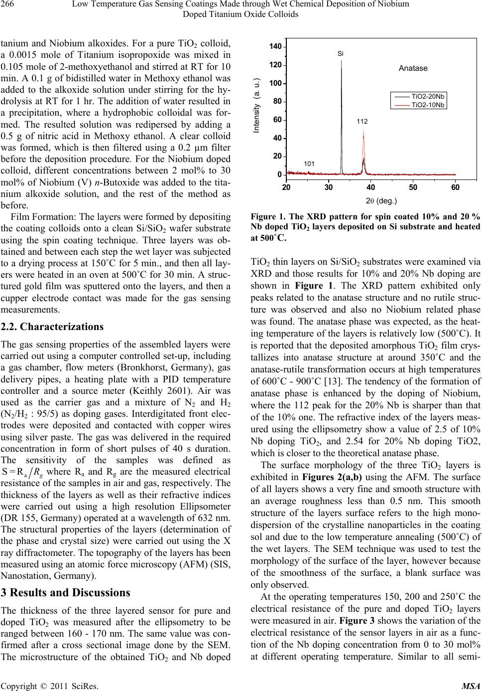 Low Temperature Gas Sensing Coatings Made through Wet Chemical Deposition of Niobium 266 Doped Titanium Oxide Colloids tanium and Niobium alkoxides. For a pure TiO2 colloid, a 0.0015 mole of Titanium isopropoxide was mixed in 0.105 mole of 2-methoxyethanol and stirred at RT for 10 min. A 0.1 g of bidistilled water in Metho xy ethanol was added to the alkoxide solution under stirring for the hy- drolysis at RT for 1 hr. The addition of water resulted in a precipitation, where a hydrophobic colloidal was for- med. The resulted solution was redipersed by adding a 0.5 g of nitric acid in Methoxy ethanol. A clear colloid was formed, which is then filtered using a 0.2 µm filter before the deposition procedure. For the Niobium doped colloid, different concentrations between 2 mol% to 30 mol% of Niobium (V) n-Butoxide was added to the tita- nium alkoxide solution, and the rest of the method as before. Film Formation: The layers were formed by depositing the coating colloids onto a clean Si/SiO2 wafer substrate using the spin coating technique. Three layers was ob- tained and between each step the wet layer was subjected to a drying process at 150˚C for 5 min., and then all lay- ers were heated in an oven at 500˚C for 30 min. A struc- tured gold film was sputtered onto the layers, and then a cupper electrode contact was made for the gas sensing measurements. 2.2. Characterizations The gas sensing properties of the assembled layers were carried out using a computer controlled set-up, including a gas chamber, flow meters (Bronkhorst, Germany), gas delivery pipes, a heating plate with a PID temperature controller and a source meter (Keithly 2601). Air was used as the carrier gas and a mixture of N2 and H2 (N2/H2 : 95/5) as doping gases. Interdigitated front elec- trodes were deposited and contacted with copper wires using silver paste. The gas was delivered in the required concentration in form of short pulses of 40 s duration. The sensitivity of the samples was defined as a S=R g Rwhere Ra and Rg are the measured electrical resistance of the samples in air and gas, respectively. The thickness of the layers as well as their refractive indices were carried out using a high resolution Ellipsometer (DR 155, Germany) operated at a wavelength of 632 nm. The structural properties of the layers (determination of the phase and crystal size) were carried out using the X ray diffractometer. The topography of the layers has been measured using an atomic force microscopy (AFM) (SIS, Nanostation, Germany). 3 Results and Discussions The thickness of the three layered sensor for pure and doped TiO2 was measured after the ellipsometry to be ranged between 160 - 170 nm. The same value was con- firmed after a cross sectional image done by the SEM. The microstructure of the obtained TiO2 and Nb doped 20 30 40 50 60 0 20 40 60 80 100 120 140 Intensity (a. u.) 2 ( de g . ) TiO2-20Nb TiO2-10Nb Anatase Si 101 112 Figure 1. The XRD pattern for spin coated 10% and 20 % Nb doped TiO2 layers deposited on Si substrate and heated at 500˚C. TiO2 thin layers on Si/SiO2 substrates were examined via XRD and those results for 10% and 20% Nb doping are shown in Figure 1. The XRD pattern exhibited only peaks related to the anatase structure and no rutile struc- ture was observed and also no Niobium related phase was found. The anatase phase was expected, as the heat- ing temperature of the layers is relatively low (500˚C). It is reported that the deposited amorphous TiO2 film crys- tallizes into anatase structure at around 350˚C and the anatase-rutile transformation occurs at high temperatures of 600˚C - 900˚C [13]. The tendency of the formation of anatase phase is enhanced by the doping of Niobium, where the 112 peak for the 20% Nb is sharper than that of the 10% one. The refractive index of the layers meas- ured using the ellipsometry show a value of 2.5 of 10% Nb doping TiO2, and 2.54 for 20% Nb doping TiO2, which is closer to the theoretical anatase phase. The surface morphology of the three TiO2 layers is exhibited in Figures 2(a,b) using the AFM. The surface of all layers shows a very fine and smooth structure with an average roughness less than 0.5 nm. This smooth structure of the layers surface refers to the high mono- dispersion of the crystalline nanoparticles in the coating sol and due to the low temperature annealing (500˚C) of the wet layers. The SEM technique was used to test the morphology of the surface of the layer, however because of the smoothness of the surface, a blank surface was only observed. At the operating temperatures 150, 200 and 250˚C the electrical resistance of the pure and doped TiO2 layers were measured in air. Figure 3 shows the variation of the electrical resistance of the sensor layers in air as a func- tion of the Nb doping concentration from 0 to 30 mol% at different operating temperature. Similar to all semi- C opyright © 2011 SciRes. MSA 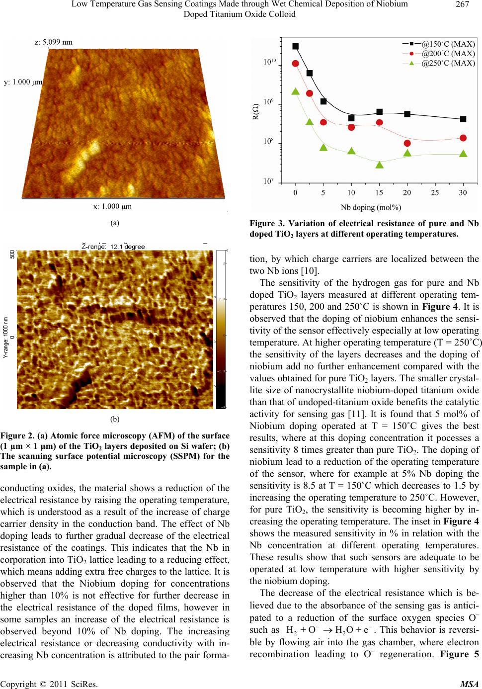 Low Temperature Gas Sensing Coatings Made through Wet Chemical Deposition of Niobium Doped Titanium Oxide Colloid Copyright © 2011 SciRes. MSA 267 Figure 3. Variation of electrical resistance of pure and Nb doped TiO2 layers at different operating temperatures. (a) tion, by which charge carriers are localized between the two Nb ions [10]. The sensitivity of the hydrogen gas for pure and Nb doped TiO2 layers measured at different operating tem- peratu res 150, 200 and 250 ˚C is shown in Figure 4. It is observed that the doping of niobium enhances the sensi- tivity of the sensor effectively especially at low operating temperature. At higher operating temperature (T = 250˚C) the sensitivity of the layers decreases and the doping of niobium add no further enhancement compared with the values obtained for pure TiO2 layers. The smaller crystal- lite size of nanocrystallite niobium-doped titanium oxide than that of undoped-titanium oxide benefits the catalytic activity for sensing gas [11]. It is found that 5 mol% of Niobium doping operated at T = 150˚C gives the best results, where at this doping concentration it pocesses a sensitivity 8 times greater than pure TiO2. The doping of niobium lead to a reduction of the operating temperature of the sensor, where for example at 5% Nb doping the sensitivity is 8.5 at T = 150˚C which decreases to 1.5 by increasing the operating temperature to 250˚C. However, for pure TiO2, the sensitivity is becoming higher by in- creasing the operating temperature. The inset in Figure 4 shows the measured sensitivity in % in relation with the Nb concentration at different operating temperatures. These results show that such sensors are adequate to be operated at low temperature with higher sensitivity by the niobium doping. (b) Figure 2. (a) Atomic force microscopy (AFM) of the surface (1 µm × 1 µm) of the TiO2 layers deposited on Si wafer; (b) The scanning surface potential microscopy (SSPM) for the sample in (a). conducting oxides, the material shows a reduction of the electrical resistance by raising the operating temperature, which is understood as a result of the increase of charge carrier density in the conduction band. The effect of Nb doping leads to further gradual decrease of the electrical resistance of the coatings. This indicates that the Nb in corporation into TiO2 lattice leading to a reducing effect, which means adding extra free charges to the lattice. It is observed that the Niobium doping for concentrations higher than 10% is not effective for further decrease in the electrical resistance of the doped films, however in some samples an increase of the electrical resistance is observed beyond 10% of Nb doping. The increasing electrical resistance or decreasing conductivity with in- creasing Nb concentration is attributed to the pair forma- The decrease of the electrical resistance which is be- lieved due to the absorbance of the sensing gas is antici- pated to a reduction of the surface oxygen species O– such as . This behavior is reversi- ble by flowing air into the gas chamber, where electron recombination leading to O– regeneration. Figure 5 – 22 H+O HO+e– 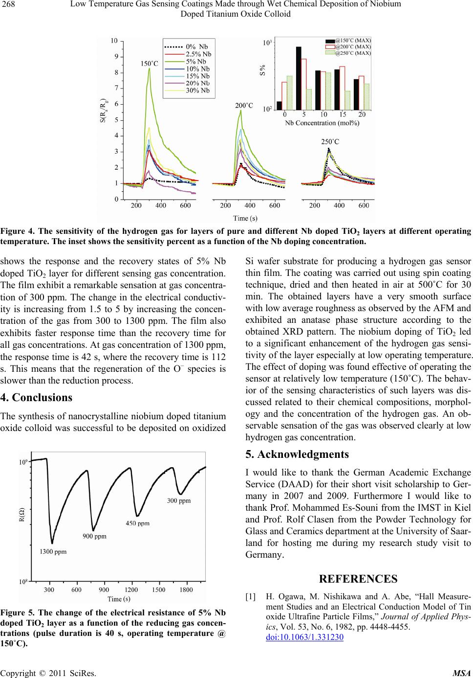 Low Temperature Gas Sensing Coatings Made through Wet Chemical Deposition of Niobium 268 Doped Titanium Oxide Colloid Figure 4. The sensitivity of the hydrogen gas for layers of pure and different Nb doped TiO2 layers at different operating temperature. The inset shows the sensitivity percent as a function of the Nb doping concentration. shows the response and the recovery states of 5% Nb doped TiO2 layer for different sensing gas concentration. The film exhibit a remarkable sensation at gas concentra- tion of 300 ppm. The change in the electrical conductiv- ity is increasing from 1.5 to 5 by increasing the concen- tration of the gas from 300 to 1300 ppm. The film also exhibits faster response time than the recovery time for all gas concentrations. At gas concentration of 1300 ppm, the response time is 42 s, where the recov ery time is 112 s. This means that the regeneration of the O– species is slower than the reduction process. 4. Conclusions The synthesis of nanocrystalline niobium doped titanium oxide colloid was successful to be deposited on oxidized Figure 5. The change of the electrical resistance of 5% Nb doped TiO2 layer as a function of the reducing gas concen- trations (pulse duration is 40 s, operating temperature @ 150˚C). Si wafer substrate for producing a hydrogen gas sensor thin film. The coating was carried out using spin coating technique, dried and then heated in air at 500˚C for 30 min. The obtained layers have a very smooth surface with low av erag e rou ghne ss as observed by the AFM and exhibited an anatase phase structure according to the obtained XRD pattern. The niobium doping of TiO2 led to a significant enhancement of the hydrogen gas sensi- tivity of the layer especially at low operating temperature. The effect of doping was found effective of operating the sensor at relatively low temperature (150˚C). The behav- ior of the sensing characteristics of such layers was dis- cussed related to their chemical compositions, morphol- ogy and the concentration of the hydrogen gas. An ob- servable sensation of the gas was observed clearly at low hydrogen gas concentration. 5. Acknowledgments I would like to thank the German Academic Exchange Service (DAAD) for their short visit scholarship to Ger- many in 2007 and 2009. Furthermore I would like to thank Prof. Mohammed Es-Souni from the IMST in Kiel and Prof. Rolf Clasen from the Powder Technology for Glass and Ceramics department at the University of Saar- land for hosting me during my research study visit to Germany. REFERENCES [1] H. Ogawa, M. Nishikawa and A. Abe, “Hall Measure- ment Studies and an Electrical Conduction Model of Tin oxide Ultrafine Particle Films,” Journal of Applied Phys- ics, Vol. 53, No. 6, 1982, pp. 4448-4455. doi:10.1063/1.331230 C opyright © 2011 SciRes. MSA  Low Temperature Gas Sensing Coatings Made through Wet Chemical Deposition of Niobium 269 Doped Titanium Oxide Colloid [2] H. Cheong and M. Lee, “Sensing Characteristics and Surface Reaction Mechanism of Alcohol Sensors Based on Doped SnO2,” Journal of Ceramic Processing Re- search, Vol. 7, No. 3, 2006, pp. 183-191. [3] C. H. Kwon, H. Hong, D. H. Yun, S. Kim, Y. Roh and H. Lee, “Thick-Film Zinc-Oxide Gas Sensor for the Control of Lean Air-to-Fuel Ratio in Domestic Combustion Sys- tems,” Sensors and Actuators B: Chemical, Vol. 25, No. 1, 1995, pp. 610-613. doi:10.1016/0925-4005(95)85134-8 [4] S. Shukla, S. Seal, L. Ludwig and C. Parish, “Nanocrys- talline Indium Oxide-Doped Tin Oxide Thin Film as Low Temperature Hydrogen Sensor,” Sensors and Actuators B: Chemical, Vol. 97, No. 2-3, 2004, pp. 256-265. doi:10.1016/j.snb.2003.08.025 [5] M. C. Corotta, M. Ferroni, D. Gnani, M. Merli, G. Ma rti- nelli, M. C. Casale and M. Notaro,” Pure and Nb-Doped TiO2 as Thick Film Gas Sensors for Environmental Monitoring,” Sensors and Actuators B: Chemical, Vol. 58, No. 1-3, 1999, pp. 310-317. doi:10.1016/S0925-4005(99)00148-3 [6] H. Schmidt, M. Akarsu, T. S. Müller, K. Moh, G. Schäfer, D. J. Strauss and M. Naumann, “The Formation of Gra- dients in Wet Deposited Coatings with Photocatalytically Active Nanoparticles,” Research on Chemical Intermedi- ates, Vol. 31, No. 4-6, 2005, pp. 535-553. doi:10.1163/1568567053956680 [7] O. Legrini, E. Oliveros and A. M. Braun, “Photochemical Processes for Water Treatment,” Chemical Reviews, Vol. 93, No. 2, 1993, pp. 671-698. doi:10.1021/cr00018a003 [8] R. Kishore, S. N. Singh and B. Das, “Screen Printed Tita- nium Oxide and PECVD Silicon Nitride as Antireflection Coating on Silicon Solar Cells,” Renewable Energy, Vol. 12, No. 2, 1997, pp. 131-135. doi:10.1016/S0960-1481(97)00030-X [9] M. Ponce, R. Parra, R. Savu, E. Joanni, P. Bueno, M. Cilense, J. Varela and M. Castro, “Impedance Spectros- copy Analysis of TiO2 Thin Film Gas Sensors Obtained from Water-Based Anatase Colloids,” Sensors and Ac- tuators B, Vol. 139, No. 2, 2009, pp. 447-452. doi:10.1016/j.snb.2009.03.066 [10] Varghese, D. Gong, M. Paulose, K. Ong and C. Grimes, “Hydrogen Sensing Using Titania Nanotubes,” Sensors and Actuators B: Chemical, Vol. 93, No. 1-3, 2003, pp. 338-344. doi:10.1016/S0925-4005(03)00222-3 [11] L. S. Hsu, R. Rujkorakarn, J. R. Sites, and C. Y. She, “Thermally Induced Crystallization of Amorphous-Titania Film”, Journal of Applied Physics, Vol. 59, No. 10, 1986, pp. 3475-3480. doi:10.1063/1.336817 [12] I. Song, “Defect Struct ure and DC Electrical Conductivity of Titanium Dioxide-Niobium Dioxide Solid Solution”, Ph.D. Thesis, Case Western Reserve University, Cleve- land, 1990. [13] M. Lee, C. Shih, S. Fang, H. Tu and C. Ho, “Preparation of Niobium-Doped Titanium Oxide Film by Liquid Phase Deposition,” Japanese Journal of Applied Physics, Vol. 46, No. 4A, 2007, pp. 1653-1655. doi:10.1143/JJAP.46.1653 C opyright © 2011 SciRes. MSA |