

Paper Menu >>
Journal Menu >>
 Journal of Computer and Communications, 2013, 1, 50-53 Published Online December 2013 (http://www.scirp.org/journal/jcc) http://dx.doi.org/10.4236/jcc.2013.17012 Open Access JCC THz Oscillations in a GaN Based Planar Nano-Device K. Y. Xu1, Y. N. Wang2, Z. N. Wang2, J. W. Xiong2, G. Wang2 1Laboratory of Quantum Information Technology, School of Physics and Telecommunication Engineering, South China Normal University, Guangzhou, China; 2State Key Laboratory of Optoelectronic Materials and Technologies, Sun Yat-sen University, Guangzhou, China. Email: [email protected] Received September 2013 ABSTRACT Gunn oscillations in a GaN based planar nano-device have been studied by ensemble Monte Carlo (EMC) method. Si- mulation results show that when the channel length of the device reduces to 450 nm, THz oscillations (about 0.3 THz) can be obtained. Also the phase of the oscillations can be controlled by the initial conditions that excite the Gunn do- mains. Moreover, through adjusting the phase difference between the oscillations in a double-channels device, which attained by parallel connecting two single-channel devices, the frequency of the device shifts from 0.3 THz to 0.6 THz. This phenomenon remains in devices with shorter channel-length, unless the channel-length is too short to support Gunn osci llations . T he possible underlying mec ha nisms are a lso discuss ed. Keywords: THz Oscillation; Gunn; Monte Carlo; GaN; Planar Nanodevice 1. Introduction The terahertz (1 THz = 1000 GHz) electromagnetic wave has attracted w ide attentions as it could enable very broad applications ranging from non-destructive imaging and spectroscopy of biological materials, remote detection of hidden objects and explosives, to manipulations of quan- tum states in semiconductors [1,2]. Moreover, develop- ment of semiconductor THz electronic devices is also cer- tainly paramount and timely to future generation of large- volume information processing and high-performance computations. However, the development of THz tech- nology is so far largely hampered by the lack of reliable, solid-state sources operating at room-temperature [3]. One possible way of developing THz devices is to adapt well-known mechanisms that have been already utilized in microwave f ield for higher frequency applica- tions. Among them, Gunn Effect in GaN is considered as one of the most promising candidates for further THz sources, which has attracted wide attention recently [4-8]. Heat dissipation is considered as one of the most chal- lenging issues for practical GaN-based Gunn sour ces. To conquer this problem, planar devices, such as SSDs [9], may be a suitable choice, since planar architecture allows easier design for heat dissipation [5,8]. In addition, in planar devices the electrodes are connected side by side to the active semiconductor layer rather than placed on top of each other, as in conventional multilayered vertical- structured devices, resulting in very low parasitic capa- citances. As such, high speeds are attainable. In this work, we focus on studying the behaviors of Gunn oscillations in GaN based SSDs at room tempera- ture. SSDs as shown in Figure 1 are planar nanodevices, which not only have high operation speed, up to THz at room temperature, but also benefit for the propagation of Gunn domains [10]. The paper is structured as follows. In Section 2, device structures and simulation models are introduced. In Section 3, the time-dependent Gunn oscil- lations are studied under different bias conditions. Then the relationship between the initial phase of the oscilla- tion and the exciting condition is established. And moreo - ver the interaction of Gunn oscillations in adjacent double channels is further studied under different phase condi- tions. In Section 4, simulation results are further dis- cussed. 2. Device Structures and EMC Model Figure 1(a) shows schematically the top view of a double-channels device including two SSDs and will be mentioned as D-SSD in follows. The device is based on a GaN/AlGaN heterostructure, where a 2DEG is formed at the hetero-interface with a carrier concentration of 8.0 × 1012 cm−2 [8]. For a single-channel SSD (S-SSD) framed by green dashed line in Figure 1(a), the two L-shaped insulating trenches are etched through the 2DEG layer, which ensures that electrons have to pass the narrow channel between the two trenches in order to conduct a 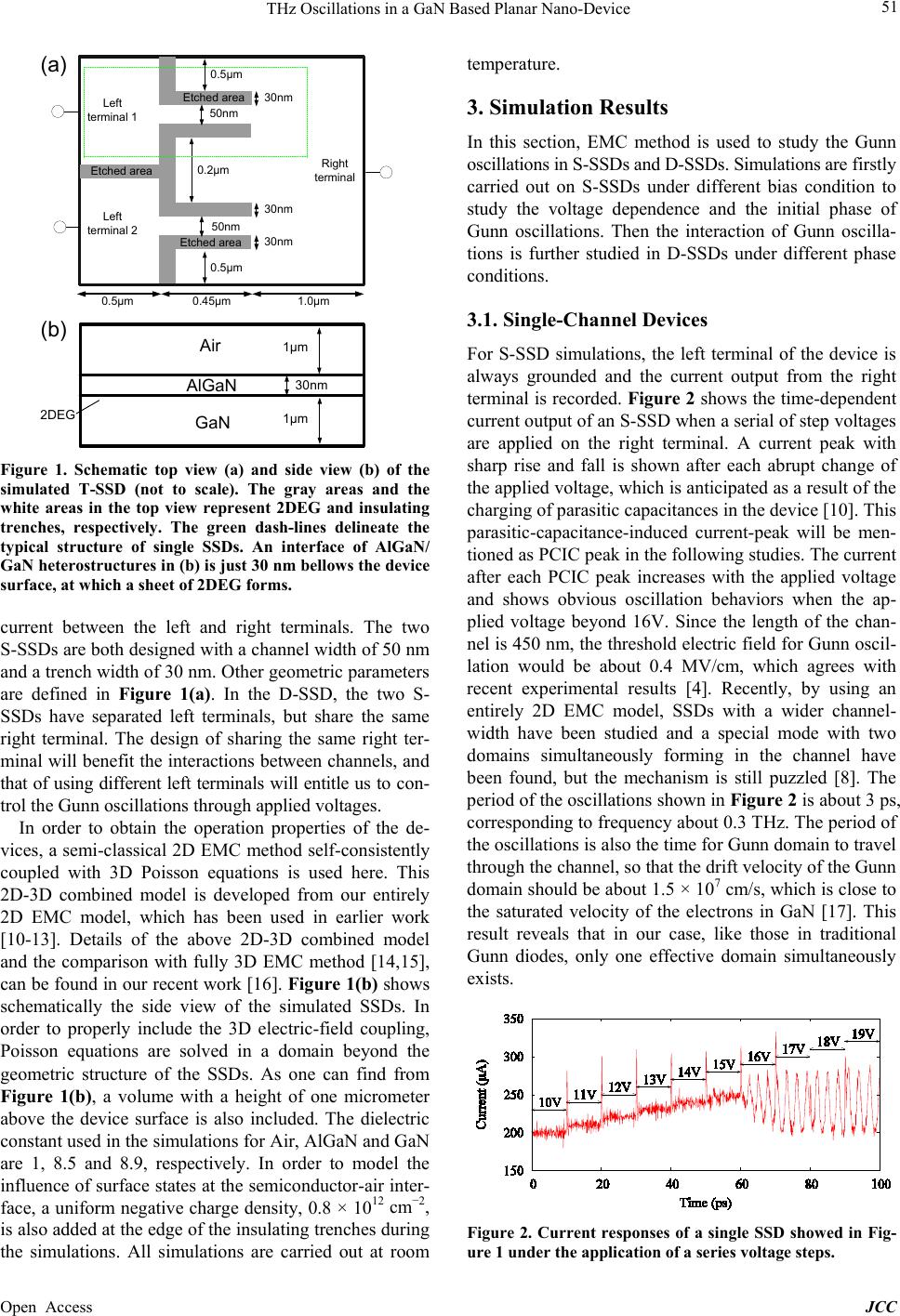 THz Oscillations in a GaN Based Planar Nano-Device Open Access JCC 51 (a) 0.5μm0.45μm 1.0μm Left terminal 2 Right terminal 50nm 30nm 0.2μm 30nm 2DEG Air 1μm 1μm GaN AlGaN Etched area Etched area Etched area 50nm Left terminal 1 30nm 30nm 0.5μm 0.5μm (b) Figure 1. Schematic top view (a) and side view (b) of the simulated T-SSD (not to scale). The gray areas and the white areas in the top view represent 2DEG and insulating trenches, respectively. The green dash-lines delineate the typical structure of single SSDs. An interface of AlGaN/ GaN heterostructures in (b) is just 30 nm bellows the de vice surface, at which a sheet of 2DEG forms. current between the left and right terminals. The two S-SSDs are both designed with a channel width of 50 nm and a trench width of 30 nm. Other geometric parameters are defined in Figure 1(a). In the D-SSD, the two S- SSDs have separated left terminals, but share the same right terminal. The design of sharing the same right ter- minal will benefit the interactions between channels, and that of using different left terminals will entitle us to con- trol the Gunn oscillations through applied voltage s . In order to obtain the operation properties of the de- vices, a semi-classical 2D EMC method self-consistently coupled with 3D Poisson equations is used here. This 2D-3D combined model is developed from our entirely 2D EMC model, which has been used in earlier work [10-13]. Details of the above 2D-3D combined model and the comparison with fully 3D EMC method [14,15], can be found in our recent work [16]. Figure 1(b) shows schematically the side view of the simulated SSDs. In order to properly include the 3D electric-field coupling, Poisson equations are solved in a domain beyond the geometric structure of the SSDs. As one can find from Figure 1(b), a volume with a height of one micrometer above the device surface is also included. The dielectric constant used in the simulations for Air, AlGaN and GaN are 1, 8.5 and 8.9, respectively. In order to model the influence of surface states at the semiconductor-air inter- face, a uniform negative charge density, 0.8 × 1012 cm−2, is also added at the edge of the insulating trenches during the simulations. All simulations are carried out at room temperature. 3. Simulation Results In this section, EMC method is used to study the Gunn oscillations in S-SSDs and D-SSDs. Sim ulations are firstly carried out on S-SSDs under different bias condition to study the voltage dependence and the initial phase of Gunn oscillations. Then the interaction of Gunn oscilla- tions is further studied in D-SSDs under different phase conditions. 3.1. Single-Channel Devices For S-SSD simulations, the left terminal of the device is always grounded and the current output from the right terminal is recorded. Fig ure 2 shows the time-dependent current output of an S-SSD when a serial of step voltages are applied on the right terminal. A current peak with sharp rise and fall is shown after each abrupt change of the applied voltage, which is anticipated as a result of the charging of parasitic capacitances in the device [10]. This parasitic-capacitance-induced current-peak will be men- tioned as PCIC peak in the following studies. The current after each PCIC peak increases with the applied voltage and shows obvious oscillation behaviors when the ap- plied voltage beyond 16V. Since the length of the chan- nel is 450 nm, the threshold electric field for Gunn os cil- lation would be about 0.4 MV/cm, which agrees with recent experimental results [4]. Recently, by using an entirely 2D EMC model, SSDs with a wider channel- width have been studied and a special mode with two domains simultaneously forming in the channel have been found, but the mechanism is still puzzled [8]. The period of the oscillations shown in Figure 2 is about 3 ps, corresponding to frequency about 0.3 THz. The period of the oscillations is also the time for Gunn domain to travel through the channel, so that the drift velocity of the Gunn domain should be about 1.5 × 107 cm/s, which is close to the saturated velocity of the electrons in GaN [17]. This result reveals that in our case, like those in traditional Gunn diodes, only one effective domain simultaneously exists. Figure 2. Current responses of a single SSD showed in Fig- ure 1 under the application of a series voltage steps. 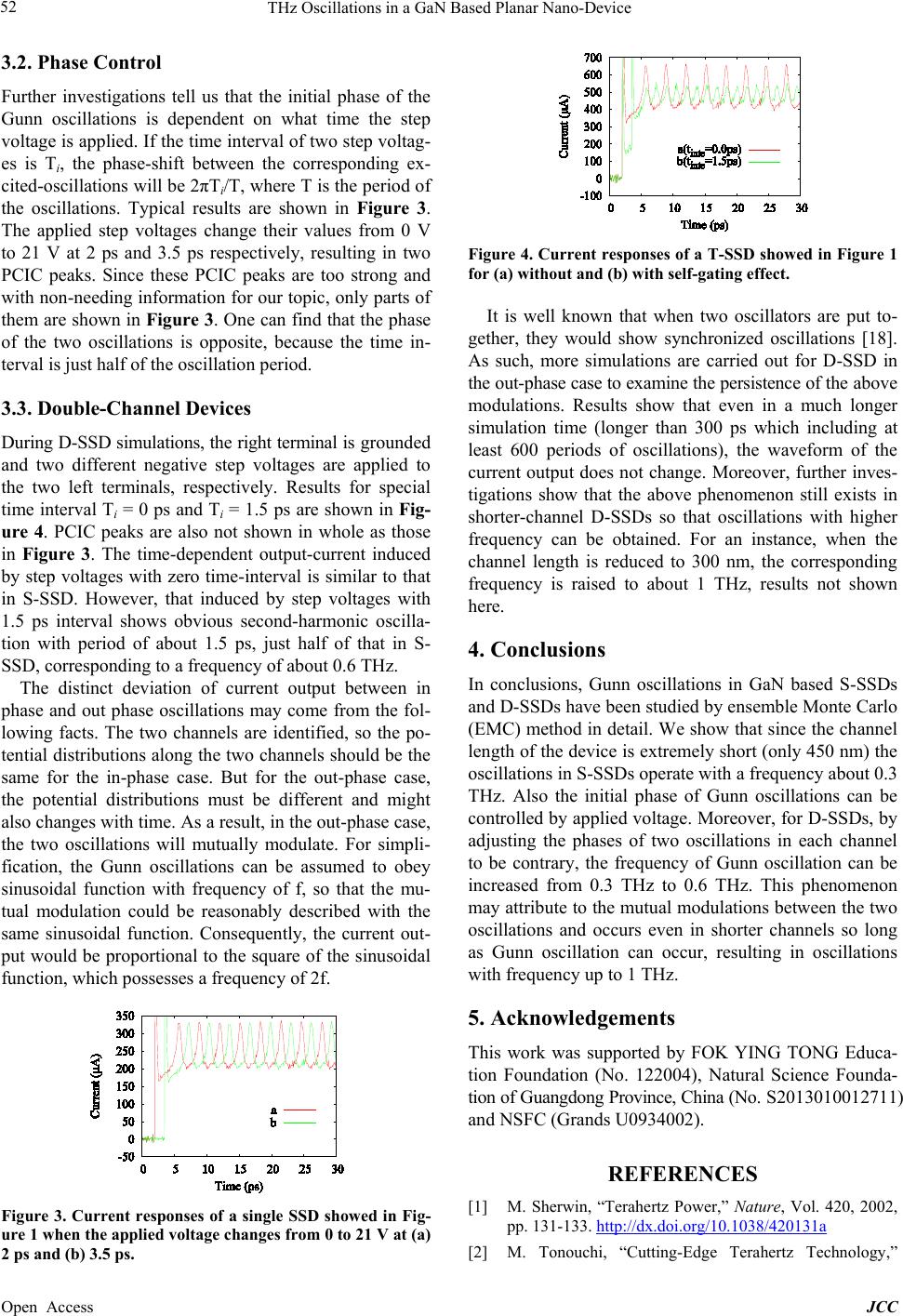 THz Oscillations in a GaN Based Planar Nano-Device Open Access JCC 52 3.2. Phase Control Further investigations tell us that the initial phase of the Gunn oscillations is dependent on what time the step voltage is applied. If the time interval of two step voltag - es is Ti, the phase-shift between the corresponding ex- cited-oscillations will be 2πTi/T, where T is the period of the oscillations. Typical results are shown in Figure 3. The applied step voltages change their values from 0 V to 21 V at 2 ps and 3.5 ps respectively, resulting in two PCIC peaks. Since these PCIC peaks are too strong and with non-needing information for our topic, only parts of them are shown in Figure 3. One can find that the phase of the two oscillations is opposite, because the time in- terval is just half of the oscillation period. 3.3. Double-Channel Devices During D-SSD simulations, the right ter minal is grounded and two different negative step voltages are applied to the two left terminals, respectively. Results for special time interval Ti = 0 ps and Ti = 1.5 ps are shown in Fig- ure 4. PCIC peaks are also not shown in whole as those in Figure 3. The time-dependent output-current induced by step voltages with zero time-interval is similar to that in S-SSD. However, that induced by step voltages with 1.5 ps interval shows obvious second-harmonic oscilla- tion with period of about 1.5 ps, just half of that in S- SSD, corresponding to a frequency of about 0.6 THz. The distinct deviation of current output between in phase and out phase oscillations may come from the fol- lowing facts. The two channels are identified, so the po- tential distributions along the two channels should be the same for the in-phase case. But for the out-phase case, the potential distributions must be different and might also changes with time. As a result, in the out -phase case, the two oscillations will mutually modulate. For simpli- fication, the Gunn oscillations can be assumed to obey sinusoidal function with frequency of f, so that the mu- tual modulation could be reasonably described with the same sinusoidal function. Consequently, the current out- put would be proportional to the square of the sinusoidal function, which possesses a fr e q uency of 2f . Figure 3. Current responses of a single SSD showed in Fig- ure 1 when the applied voltage changes from 0 to 21 V at (a) 2 ps and (b) 3.5 ps. Figure 4. Current re sponses of a T-SSD showed in Figure 1 for (a) without and (b) with self-gating effect. It is well known that when two oscillators are put to- gether, they would show synchronized oscillations [18]. As such, more simulations are carried out for D-SSD in the out-phase case to exa mine the persis tence of the above modulations. Results show that even in a much longer simulation time (longer than 300 ps which including at least 600 periods of oscillations), the waveform of the current output does not change. Moreover, further inves- tigations show that the above phenomenon still exists in shorter-channel D-SSDs so that oscillations with higher frequency can be obtained. For an instance, when the channel length is reduced to 300 nm, the corresponding frequency is raised to about 1 THz, results not shown here. 4. Conclusions In conclusions, Gunn oscillations in GaN based S-SSDs and D-SSDs have been studied by ensemble Monte Carlo (EMC) method in detail. We show that since the channel length of the device is extremely short (only 450 nm) the oscillations in S-SSDs operate with a frequency about 0.3 THz. Also the initial phase of Gunn oscillations can be controlled by applied voltage. Moreover, for D-SSD s, by adjusting the phases of two oscillations in each channel to be contrary, the frequency of Gunn oscillation can be increased from 0.3 THz to 0.6 THz. This phenomenon may attribute to the mutual modulations between the two oscillations and occurs even in shorter channels so long as Gunn oscillation can occur, resulting in oscillations with frequency up to 1 THz. 5. Acknowledgements This work was supported by FOK YING TONG Educa- tion Foundation (No. 122004), Natural Science Founda- tion of Guangdong Province, China (No. S2013010012711) and NSFC (Grands U0934002). REFERENCES [1] M. Sherwin, “Terahertz Power,” Nature, Vol. 420, 2002, pp. 131-133. http://dx.doi.org/10.1038/420131a [2] M. Tonouchi, “Cutting-Edge Terahertz Technology,” 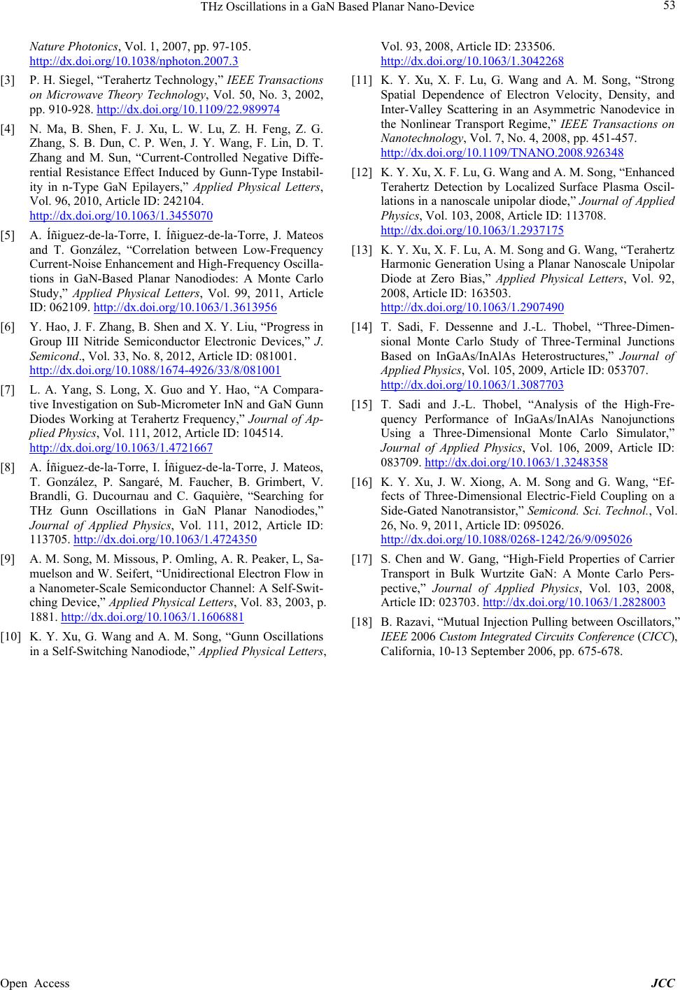 THz Oscillations in a GaN Based Planar Nano-Device Open Access JCC 53 Nature Photonics, Vol. 1, 2007, pp. 97-105. http://dx.doi.org/10.1038/nphoton.2007.3 [3] P. H. Siegel, “Terahertz Technology,” IEEE Transactions on Microwave Theory Technology, Vol. 50, No. 3, 2002, pp. 910-928. http://dx.doi.org/10.1109/22.989974 [4] N. Ma, B. Shen, F. J. Xu, L. W. Lu, Z. H. Feng, Z. G. Zhang, S. B. Dun, C. P. Wen, J. Y. Wang, F. Lin, D. T. Zhang and M. Sun, “Current-Controlled Negative Diffe- rential Resistance Effect Induced by Gunn-Type Instabil- ity in n-Type GaN Epilayers,” Applied Physical Letters, Vol. 96, 2010, Article ID: 242104. http://dx.doi.org/10.1063/1.3455070 [5] A. Íñiguez-de-la-Torre, I. Íñiguez-de-la-Torre, J. Mateos and T. González, “Correlation between Low-Frequency Current-Noise Enhancement and High-Frequency Oscilla- tions in GaN-Based Planar Nanodiodes: A Monte Carlo Study,” Applied Physical Letters, Vol. 99, 2011, Article ID: 062109. http://dx.doi.org/10.1063/1.3613956 [6] Y. Hao, J. F. Zhang, B. Shen and X. Y. Liu, “Progress in Group III Nitride Semiconductor Electronic Devices,” J. Semicond., Vol. 33, No. 8, 2012, Article ID: 081001. http://dx.doi.org/10.1088/1674-4926/33/8/081001 [7] L. A. Yang, S. Long, X. Guo and Y. Hao, “A Compara- tive Investigation on Sub-Micrometer InN and GaN Gunn Diodes Working at Terahertz Frequency,” Journal of Ap- plied Physics, Vol. 111, 2012, Article ID: 104514. http://dx.doi.org/10.1063/1.4721667 [8] A. Íñiguez-de-la-Torre, I. Íñiguez-de-la-Torre, J. Mateos, T. González, P. Sangaré, M. Faucher, B. Grimbert, V. Brandli, G. Ducournau and C. Gaquière, “Searching for THz Gunn Oscillations in GaN Planar Nanodiodes,” Journal of Applied Physics, Vol. 111, 2012, Article ID: 113705. http://dx.doi.org/10.1063/1.4724350 [9] A. M. Song, M. Missous, P. Omli ng, A. R. Peaker, L, Sa - muelson and W. Seifert, “Unidirectional Electron Flow in a Nanometer-Scale Semiconductor Channel: A Sel f-Swit- ching Device,” Applied Physical Letters, Vol. 83, 2003, p. 1881. http://dx.doi.org/10.1063/1.1606881 [10] K. Y. Xu, G. Wang and A. M. Song, “Gunn Oscillations in a Self-Switching Nanodiode,” Applied Physical Letters, Vol. 93, 2008, Article ID: 233506. http://dx.doi.org/10.1063/1.3042268 [11] K. Y. Xu, X. F. Lu, G. Wang and A. M. Song, “Strong Spatial Dependence of Electron Velocity, Density, and Inter-Valley Scattering in an Asymmetric Nanodevice in the Nonlinear Transport Regime,” IEEE Transactions on Nanotechnology, Vol. 7, No. 4, 2008, pp. 451-457. http://dx.doi.org/10.1109/TNANO.2008.926348 [12] K. Y. Xu, X. F. Lu, G. Wang and A. M. Song, “Enhanced Terahertz Detection by Localized Surface Plasma Oscil- lations in a nanoscale unipolar diode,” Journal of Applied Physics, Vol. 103, 2008, Article ID: 113708. http://dx.doi.org/10.1063/1.2937175 [13] K. Y. Xu, X. F. Lu, A. M. Song and G. Wang, “Terahertz Harmonic Generation Using a Planar Nanoscale Unipolar Diode at Zero Bias,” Applied Physical Letters, Vol. 92, 2008, Article ID: 163503. http://dx.doi.org/10.1063/1.2907490 [14] T. Sadi, F. Dessenne and J.-L. Thobel, “Three-Dimen- sional Monte Carlo Study of Three-Terminal Junctions Based on InGaAs/InAlAs Heterostructures,” Journal of Applied Physics, Vol. 105, 2009, Article ID: 053707. http://dx.doi.org/10.1063/1.3087703 [15] T. Sadi and J.-L. Thobel, “Analysis of the High-Fre- quency Performance of InGaAs/InAlAs Nanojunctions Using a Three-Dimensional Monte Carlo Simulator,” Journal of Applied Physics, Vol. 106, 2009, Article ID: 083709. http://dx.doi.org/10.1063/1.3248358 [16] K. Y. Xu, J. W. Xiong, A. M. Song and G. Wang, “Ef- fects of Three-Dimensional Electric-Field Coupling on a Side-Gated Nanotransistor,” Semicond. Sci. Technol., Vol. 26, No. 9, 2011, Article ID: 095026. http://dx.doi.org/10.1088/0268-1242/26/9/095026 [17] S. Chen and W. Gang, “High-Field Properties of Carrier Transport in Bulk Wurtzite GaN: A Monte Carlo Pers- pective,” Journal of Applied Physics, Vol. 103, 2008, Article ID: 023703. http://dx.doi.org/10.1063/1.2828003 [18] B. Razavi, “Mutual Injection Pulling between Oscillators,” IEEE 2006 Custom Int egrated Circuits Conference (CICC), California, 10-13 September 2006, pp. 675-678. |