

Paper Menu >>
Journal Menu >>
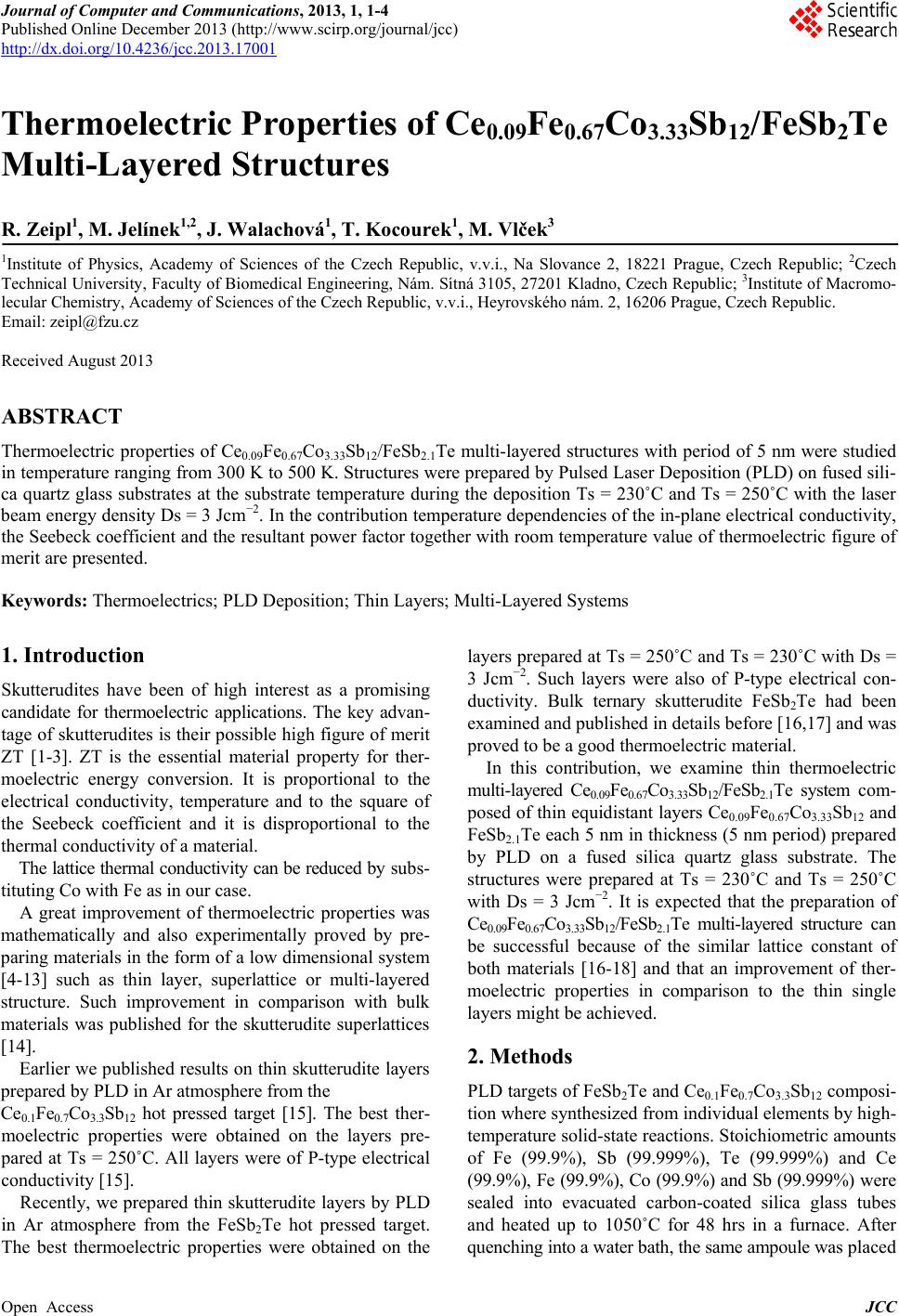 Journal of Computer and Communications, 2013, 1, 1-4 Published Online December 2013 (http://www.scirp.org/journal/jcc) http://dx.doi.org/10.4236/jcc.2013.17001 Open Access JCC 1 Thermoelectric Properties of Ce0.09Fe0.67Co3.33Sb12/FeSb2Te Multi-Layered Structures R. Zeipl1, M. Jelínek1,2, J. Walachová1, T. Kocourek1, M. Vlček3 1Institute of Physics, Academy of Sciences of the Czech Republic, v.v.i., Na Slovance 2, 18221 Prague, Czech Republic; 2Czech Technical University, Fa culty of Biomedical Engineering, Nám. Sítná 3105, 27201 Kladno, Czech Republic; 3Institute of Macromo- lecular Chemistry, Academy of Sciences of the Czech Republic, v.v.i., Heyrovského nám. 2, 16206 Prague, Czech Republic. Email: [email protected] Received August 2013 ABSTRACT Thermoelectric properties of Ce0.09Fe0.67Co3.33Sb12/FeSb2.1Te multi-layered structures with period of 5 nm were studied in temperature ranging from 300 K to 500 K. Structures were prepared by Pulsed Laser Deposition (PLD) on fused sili- ca quartz glass substrates at the substrate temperature during the deposition Ts = 230˚C and Ts = 250˚C with the laser beam energy density Ds = 3 Jcm−2. In the contribution temperature dependencies of the in-plane electrical conductivity, the Seebeck coefficient and the resultant power factor together with room temperature value of thermoelectric figure of merit are presented. Keywords: Thermoelectrics; PLD Deposition; Thin Lay ers; Multi-Layered Systems 1. Introduction Skutterudites have been of high interest as a promising candidate for thermoelectric applications. The key advan- tage of skutterudites is their possible high figure of merit ZT [1-3]. ZT is the essential material property for ther- moelectric energy conversion. It is proportional to the electrical conductivity, temperature and to the square of the Seebeck coefficient and it is disproportional to the thermal conductivity of a material. The lattice thermal conductivity can be reduced by subs- tituting Co with Fe as in our case. A great improvement of thermoelectric properties was mathematically and also experimentally proved by pre- paring materials in the form of a low dimensional system [4-13] such as thin layer, superlattice or multi-layered structure. Su ch improvement in comparison with bulk materials was published for the skutterudite superlattices [14]. Earlier we published results on thin skutterudite layers prepared by PLD in Ar atmosphere from the Ce0.1Fe0.7Co3.3Sb12 hot pressed target [15]. The best ther- moelectric properties were obtained on the layers pre- par ed at Ts = 250˚C. All layers were of P-type electrical conductivity [15]. Recently, we prepared thin skutterudite layers by PLD in Ar atmosphere from the FeSb2Te hot pressed target. The best thermoelectric properties were obtained on the layers prepared at Ts = 250˚C and Ts = 230˚C with Ds = 3 J cm−2. Such layers were also of P-typ e electrical con- ductivity. Bulk ternary skutterud ite FeSb2Te had been examined and published in details before [16,17] and was proved to be a good thermoelectric material. In this contribution, we examine thin thermoelectric multi-layered Ce0.09Fe0.67Co3.33Sb12/FeSb2.1Te system com- posed of thin equidistant layers Ce0.09Fe0.67Co3.33Sb12 and FeSb2.1Te each 5 nm in thickness (5 nm period) prepared by PLD on a fused silica quartz glass substrate. The structures were prepared at Ts = 230˚C and Ts = 250˚C with Ds = 3 Jcm−2. It is expected that the preparation of Ce0.09Fe0.67Co3.33Sb12/FeSb2.1Te multi-layered structure can be successful because of the similar lattice constant of both materials [16-18] and that an improvement of ther- moelectric properties in comparison to the thin single layers might be achieved. 2. Methods PLD targets of FeSb2Te and Ce0.1Fe0.7Co3.3Sb12 composi- tion where synthesized from individual elements by high- temperature solid-state reactions. Stoichiometric amounts of Fe (99.9%), Sb (99.999%), Te (99.999%) and Ce (99.9%), Fe (99.9%), Co (99.9%) and Sb (99.999%) were sealed into evacuated carbon-coated silica glass tubes and heated up to 1050˚C for 48 hrs in a furnace. After quenching into a water bath, the same ampoule was placed 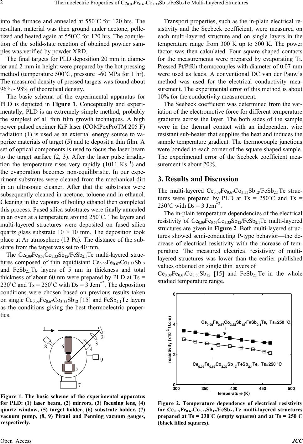 Thermoelectric Properties of Ce0.09Fe0.67Co3.33Sb12/FeSb2Te M ul ti-Layered Structures Open Access JCC 2 into the furnace and annealed at 550˚C for 120 hrs. The resultant material was then ground under acetone, pelle- tized and heated again at 550˚C for 120 hrs. The comple- tion of the solid-state reaction of obtained powder sam- ples was verified by powder XRD. The final targets for PLD deposition 20 mm in diame- ter and 2 mm in height were prepared by the hot pressing method (temperature 500˚C, pressure ~60 MPa for 1 hr). The measured density of pressed targets was found about 96% - 98% of theoretical density. The basic schema of the experimental apparatus for PLD is depicted in Figure 1. Conceptually and experi- mentally, PLD is an extremely simple method, probably the simplest of all thin film growth techniques. A high power pulsed excimer KrF laser (COMPexProTM 205 F) radiation (1) is used as an external energy source to va- porize materials of target (5) and to deposit a thin film. A set of optical components is used to focus the laser beam to the target surface (2, 3). After the laser pulse irradia- tion the temperature rises very rapidly (101 1 Ks−1) and the evaporation becomes non-equilibristic. In our expe- riment substrates were cleaned from the mechanical dirt in an ultrasonic cleaner. After that the substrates were subsequently cleaned in acetone, toluene and in ethanol. Cleaning in the vapours of boiling ethanol then completed this process. Fused silica subs trates were finally annealed in an oven at a temperature around 250 ˚C. The layers and multi-layered structures were deposited on fused silica quartz glass substrate 10 × 10 mm. The deposition took place at Ar atmosphere (13 Pa). The distance of the sub- strate from the target was set to 40 mm. The Ce0.09Fe0.67Co3.33Sb12/FeSb2.1Te multi-layered stru c- tures composed of thin equidistant Ce0.09Fe0.67Co3.33Sb12 and FeSb2.1Te layers of 5 nm in thickness and total thickness of about 60 nm were prepared by PLD at Ts = 230˚C and Ts = 250˚C with Ds = 3 Jcm−2. The deposition conditions were chosen based on previous results taken on single Ce0.09Fe0.67Co3.33Sb12 [15] and FeSb2.1Te layers as the conditions giving the best thermoelectric proper- ties. Figure 1. The basic scheme of the experimental apparatus for PLD: (1) laser beam, (2) mirrors, (3) focusing lens, (4) quartz window, (5) target holder, (6) substrate holder, (7) vacuum pump, (8, 9) Pirani and Penning vacuum gauges, respectively. Transport properties, such as the in-plain electrical re- sistivity and the Seebeck coefficient, were measured on each multi-layered structure and on single layers in the temperature range from 300 K up to 500 K. The power factor was then calculated. Four square shaped contacts for the measurements were prepared by evaporating Ti. Pressed Pt/PtRh thermocouples with diameter of 0.07 mm were used as leads. A conventional DC van der Pauw ’s method was used for the electrical conductivity mea- surement. The experimental error of this method is about 10% for the conductivity measurement. The Seebeck coefficient was determined from the var- iation of the electromotive force for different temperature gradients across the layer. The both sides of the sample were in the thermal contact with an independent wire resistant sub-heater that supplies the heat and induces the sample temperature gradient. The thermocouple junctions were bonded to each corner of the square shaped sample. The exper imental error of the Seebeck coefficient mea- surement is about 20%. 3. Results and Discussion The multi-layered Ce0.09Fe0.67Co3.33Sb12/FeSb2.1Te struc- tures were prepared by PLD at Ts = 250˚C and Ts = 230˚C with Ds = 3 Jcm−2. The in-plain temperature dependencies of the electrical resistivity of Ce0.09Fe0.67Co3.33Sb12/FeSb2.1Te multi-layered structures are given in Figure 2. Both multi-layered struc- tures showed semi-conducting P-typ e behavior—the de- crease of electrical resistivity with the increase of tem- perature. The measured electrical resistivity of multi- layered structures was lo wer than the earlier published values obtained on single thin layers of Ce0.09Fe0.67Co3.33Sb12 [15] and FeSb2.1Te in the whole studied temperature range. Figure 2. Temperature dependency of electrical resistivity for Ce0.09Fe0.67Co3.33Sb12/FeSb2.1Te multi-layered structures prepared at Ts = 230˚C (empty squares) and at Ts = 250˚C (black fil led squares). 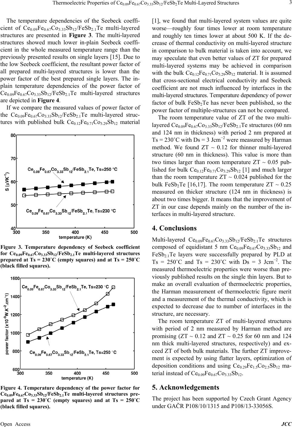 Thermoelectric Properties of Ce0.09Fe0.67Co3.33Sb12/FeSb2Te M ul ti-Layered Structures Open Access JCC 3 The temperature dependencies of the Seebeck coeffi- cient of Ce0.09Fe0.67Co3.33Sb12/FeSb2.1Te multi-layered structures are presented in Figure 3. The multi-layered structures showed much lower in-plain Seebeck coeffi- cient in the whole measured temperature range than the previously presented results on single layers [15]. Due to the low Seebeck coefficient, the resultant power factor of all prepared multi-layered structure s is lower than the power factor of the best prepared single layers. The in- plain temperature dependencies of the power factor of Ce0.09Fe0.67Co3.33Sb12/FeSb2.1Te multi-layered structures are depicted in Figure 4. If we compare the measured values of power factor of the Ce0.09Fe 0.67Co3.33Sb12/FeSb2.1Te multi-layered struc- tures with publishe d bulk Ce0.12Fe0.71Co3.29Sb12 material Figure 3. Temperature dependency of Seebeck coefficient for Ce0.09Fe0.67Co3.33Sb12/FeSb2.1Te multi-layered structures prepared at Ts = 230˚C (empty squares) and at Ts = 250˚C (black fil led squares). Figure 4. Temperature dependency of the power factor for Ce0.09Fe0.67Co3.33Sb12/FeSb2.1Te multi-layered structures pre- pared at Ts = 230˚C (empty squares) and at Ts = 250˚C (black fil led squares). [1], we found that multi-layered system values are quite worse—roughly four times lower at room temperature and roughly ten times lower at about 500 K. If the de- crease of thermal conductivity on multi-layered structure in comparison to bulk material is taken into account, we may speculate that even better values of ZT for prepared multi-layered systems may be achieved in comparison with the bulk Ce0.12Fe0.71Co3. 29Sb12 material. It is assumed that cross-sectional electrical conduc tivity and Seebeck coefficient are not much influenced by interfaces in the multi-layered stru ctures. Temperature dependenc y of power factor of bulk FeSb2Te has never been published, so the power factor of multiple-structures can not be compared. The room temperature value of ZT of the two multi- layered Ce0.09Fe0.67Co3.33Sb12/FeSb2.1Te structures (60 nm and 124 nm in thickness) with period 2 nm prepare d at Ts = 230˚C with Ds = 3 Jcm−2 were measured by Harman method. We found ZT ~ 0.12 for thinner multi-layered structure (60 nm in thickness). This value is more than two times larger than room temperature ZT ~ 0.05 pub- lished for bulk Ce0.12Fe0.71Co3.29Sb12 [1] and much larger than the room temperatu re ZT ~ 0.024 published for the bulk FeSb2Te [16,17]. The room temperature ZT ~ 0.25 measured on thicker structure (124 nm in thickness) is about two times bigger. It means that the improvement of ZT in our case depends mainly on the number of the in- terfaces in multi-layered structure. 4. Conclusions Multi-layered Ce0.09Fe0.67Co3.33Sb12/FeSb2.1Te structures composed of equidistant 5 nm Ce0.09Fe0.67Co3.33Sb12 and FeSb2.1Te layers were successfully prepared by PLD at Ts = 250˚C and Ts = 230˚C with Ds = 3 Jcm−2. The measured thermoelectric properties were wor se than pre- viously published results on the single thin layers. But to make an overall evaluation of thermoelectric properties, the Harman measurement of thermoelectric figure merit and a measurement of the thermal conductivity, which is expected to decrease due to number of interfaces in the structure, are necessary. The roo m temperature ZT of multi-layered structures with period of 2 nm measured by Harman method are promising (ZT ~ 0.12 and ZT ~ 0.25 for 60 nm and 124 nm thick multi-layered structures, respectively) and ex- ceed ZT of both bulk materials. The further ZT improve- ment is expected by using flatter layers, optimization of deposition conditions and using Ce0.29Fe1.5Co2.5Sb12 ma- terial instead of Ce0.09Fe0.67Co3.33Sb12. 5. Acknowledgements The project has been suppor te d by Czech Grant Agency under GAČR P108/10/1315 and P108/13-33056S. 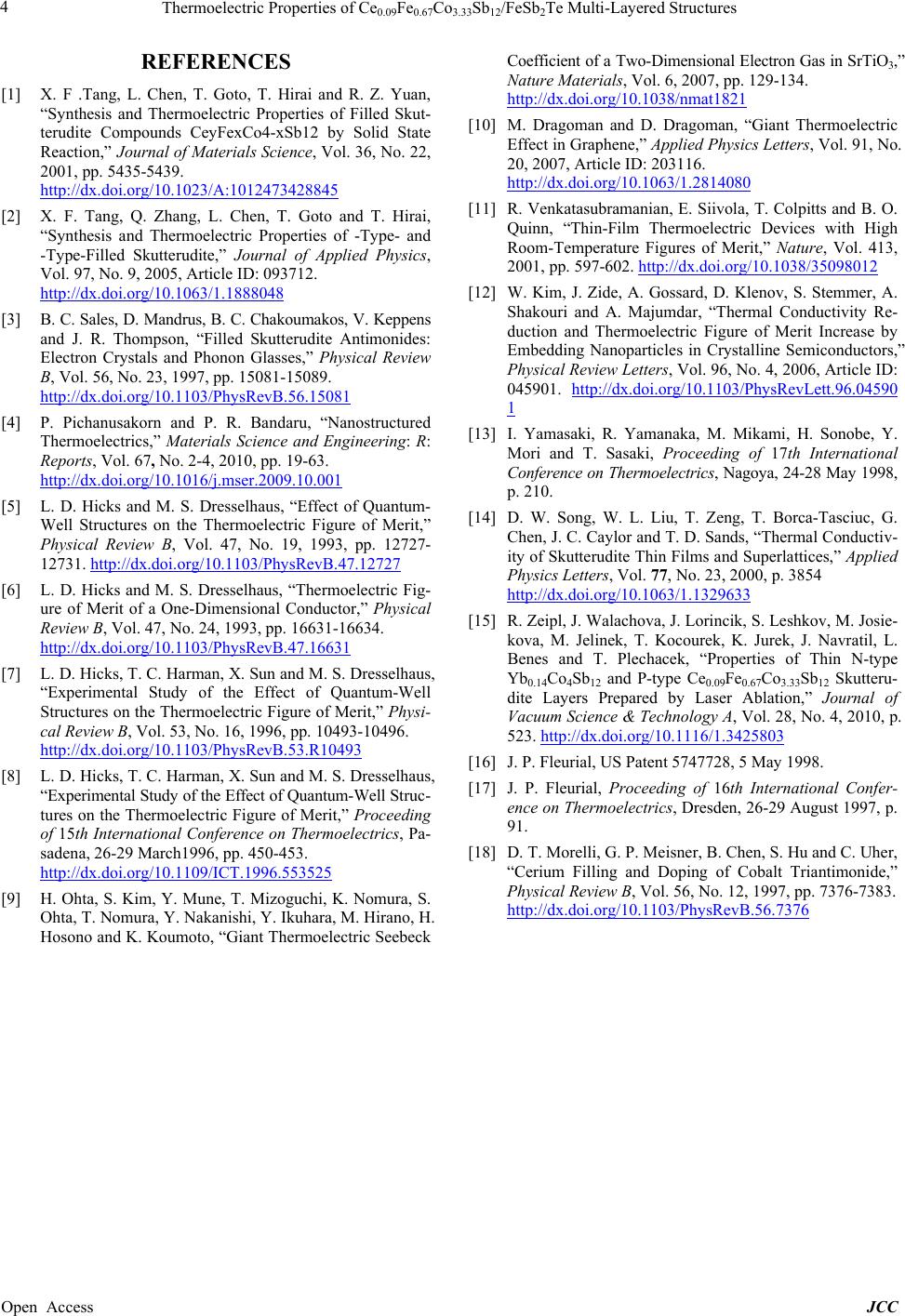 Thermoelectric Properties of Ce0.09Fe0.67Co3.33Sb12/FeSb2Te M ul ti-Layered Structures Open Access JCC 4 REFERENCES [1] X. F .Tang, L. Chen, T. Goto, T. Hirai and R. Z. Yuan, “Synthesis and Thermoelectric Properties of Filled Skut- terudite Compounds CeyFexCo4-xSb12 by Solid State Reaction,” Journal of Materials Science, Vol. 36, No. 22, 2001, pp. 5435-5439. http://dx.doi.org/10.1023/A:1012473428845 [2] X. F. Tang, Q. Zhang, L. Chen, T. Goto and T. Hirai, “Synthesis and Thermoelectric Properties of -Type- and -Type-Filled Skutterudite,” Journal of Applied Physics, Vol. 97, No. 9, 2005, Article ID: 093712. http://dx.doi.org/10.1063/1.1888048 [3] B. C. Sa le s, D. Mandru s, B. C. Chakoumakos, V. Keppens and J. R. Thompson, “Filled Skutterudite Antimonides: Electron Crystals and Phonon Glasses,” Physical Review B, Vol. 56, No. 23, 1997, pp. 15081-15089. http://dx.doi.org/10.1103/PhysRevB.56.15081 [4] P. Pichanusakorn and P. R. Bandaru, “Nanostructured Thermoelectrics,” Materials Science and Engineering: R: Reports, Vol. 67, No. 2-4, 2010, pp. 19-63. http://dx.doi.org/10.1016/j.mser.2009.10.001 [5] L. D. Hicks and M. S. Dresselhaus, “Effect of Quantum- Well Structures on the Thermoelectric Figure of Merit,” Physical Review B, Vol. 47, No. 19, 1993, pp. 12727- 12731. http://dx.doi.org/10.1103/PhysRevB.47.12727 [6] L. D. H icks and M. S. Dresselhaus, “Thermoelectric Fig- ure of Merit of a One-Dimensional Conductor,” Physical Review B, Vol. 47, No. 24, 1993, pp. 16631-16634. http://dx.doi.org/10.1103/PhysRevB.47.16631 [7] L. D. Hicks, T. C. Harman, X. Sun and M. S. Dresse lhaus, “Experimental Study of the Effect of Quantum-Well Structures on the Thermoelectric Figure of Merit,” Physi- cal Review B, Vol. 53, No. 16, 1996, pp. 10493-10496. http://dx.doi.org/10.1103/PhysRevB.53.R10493 [8] L. D. Hicks, T. C. Harman, X. Sun and M. S. Dresse lhaus, “Experimental St udy of the Effect of Quantu m-Well Struc- tures on the Thermoelectric Figure of Merit,” Proceeding of 15th International Conference on Thermoelectrics, Pa- sadena, 26-29 March1996, pp. 450-453. http://dx.doi.org/10.1109/ICT.1996.553525 [9] H. Ohta, S. Kim, Y. Mune, T. Mizoguchi, K. Nomura, S. Ohta, T. Nomura, Y. Nakanishi, Y. Ikuhara, M. Hirano, H. Hosono and K. Koumoto, “Giant T hermoelectric Seebeck Coefficient of a Two-Dimensional Electron Gas in SrTiO3,” Nature Materials, Vol. 6, 2007, pp. 129-134. http://dx.doi.org/10.1038/nmat1821 [10] M. Dragoman and D. Dragoman, “Giant Thermoelectric Effect in Graphene,” Applied Physics Letters, Vol. 91, No. 20, 2007, Article ID : 203116. http://dx.doi.org/10.1063/1.2814080 [11] R. Venkatasubramanian, E. Siivola, T. Colpitts and B. O. Quinn, “Thin-Film Thermoelectric Devices with High Room-Temperature Figures of Merit,” Nature, Vol. 413, 2001, pp. 597-602. http://dx.doi.org/10.1038/35098012 [12] W. Kim, J. Zide , A. Gossard, D. Klenov, S. Stemmer, A. Shakouri and A. Majumdar, “Thermal Conductivity Re- duction and Thermoelectric Figure of Merit Increase by Embedding Nanoparticles in Crystalline Semiconductors,” Physical Review Letters, Vol . 96, No. 4, 2006, Article ID: 045901. http://dx.doi.org/10.1103/PhysRevLett.96.04590 1 [13] I. Yamasaki, R. Yamanaka, M. Mikami, H. Sonobe, Y. Mori and T. Sasaki, Proceeding of 17th International Conference on Thermoelectrics, Nagoya, 24-28 May 1998, p. 210. [14] D. W. Song, W. L. Liu, T. Zeng, T. Borca-Tasciuc, G. Chen, J. C. Caylor and T. D. Sands, “Thermal Conductiv- ity of Skutterudite Thin Films and Superlattices,” Applied Physics Letters, Vol. 77, No. 23, 2000, p. 3854 http://dx.doi.org/10.1063/1.1329633 [15] R. Zeipl, J. Walachova, J. Lorincik, S. Leshkov, M. Josie- kova, M. Jelinek, T. Kocourek, K. Jurek, J. Navra til, L. Benes and T. Plechacek, “Properties of Thin N-type Yb0.14Co4Sb12 and P-type Ce0.09Fe0.67Co3.33Sb12 Skutteru- dite Layers Prepared by Laser Ablation,” Journal of Vacuum Science & Technology A, Vol. 28, No. 4, 2010, p. 523. http://dx.doi.org/10.1116/1.3425803 [16] J. P. Fleurial, US Patent 5747728, 5 May 1998. [17] J. P. Fleurial, Proceeding of 16th International Confer- ence on Thermoelectrics, Dresden, 26-29 August 1997, p. 91. [18] D. T. Morelli, G. P. Meisner, B. Chen, S. Hu and C. Uher, “Cerium Filling and Doping of Cobalt Triantimonide,” Physical Review B, Vol. 56, No. 12, 1997, pp. 7376-7383. http://dx.doi.org/10.1103/PhysRevB.56.7376 |