

Paper Menu >>
Journal Menu >>
 Journal of Computer and Communications, 2013, 1, 37-40 Published Online November 2013 (http://www.scirp.org/journal/jcc) http://dx.doi.org/10.4236/jcc.2013.16007 Open Access JCC 37 A Timing Skew Calibration Scheme in Time-Interleaved ADC Jing Li, Yang Liu, Hao Liu, Shuangyi Wu, Ning Ning, Qi Yu State Key Lab of Electronic Thin Films and Integrated Devices, University of Electronic Science and Technology of China, Chengdu, China. Email: [email protected] Received November 2013 ABSTRACT This paper proposes a digital background calibration scheme for timing skew in time-interleaved analog-to-digital con- verters (TIADCs). It detects the relevant timing error by subtracting the output difference with the sum of the first de- rivative of the digital o utput. The least-mean -square (LMS) loop is exploited to compensate the timing skew. Since the calibration scheme depends on the digital output, all timing skew sources can be calibrated and the main ADC is main- tained. The proposed scheme is effective within the entire frequency range of 0 − fs/2. Compared with traditional cali- bration schemes, the proposed approach is more feasible and consumes significantly lesser power and smaller area. Keywords: Timing Skew; Background Calibr ation ; Time-Interleaved; Analog-to-Digital Converters 1. Introduction Ti me-interleaved ADCs are widely used in modern com- munication systems. It is an effective way to realize high resolution and high sampling frequency by paralleling several low-speed but accurate ADCs [1-3]. Time-inter- leaving can also achieve better power consumption for Giga-Herz ADCs compared to traditional ADC architec- tures. However, because of the process, voltage and tem- perature variations, the ADC channels are not identical and the performance of the TIADC is limited by the off- set, gain and timing mismatches among the ADC chan- nels [4]. For the offset and gain mismatches, they are much easier to be compensated based on the equalization technique in the digital domain [5]. However, the timing mismatch is difficult to calibrate since it is relative with the input signal frequency. The front-end sampler is the radical way to eliminate the timing mismatches whereas it is limited by the process imposed maximum speed and charge injection [6]. Zero-crossing technique was adopted to detect and compensate the timing mismatch [7]. Reconstruction technique based on the interpolating filter was also exploited [8,9]. Although the above me- thods are useful, it sacrifices the design complexity or power consumption to trade for the good performance. In this paper, we propose a simple background calibra- tion method to compensate the timing mismatch. It is effective in the whole Nyquist bandwidth and adaptive to any types of channel ADCs. The rest of this paper is or- ganized as follows. In Section 2, the principle of the tim- ing mismatch detection and the compensation loop are presented. Section 3 provides the simulation results. Lastly, Section 4 gives the conclusions. 2. Proposed Timing Mismatch Calibration Scheme An M-channel TIADC without offset and gain mis- matches are shown in Figure 1. With interleaving, each channel ADC samples at a rate of fs/M and the overall sampling rate of the TIADC is fs. The analog input Vin(t) is band limited from DC to the Nyquist frequency with zero mean. ( )() cos in Vin tAwt=⋅⋅ (1) The digital output of the ith-channel ADC can be ex- pressed as ( ) ( ) , cos i kinsiin yAwkMi Ttw=⋅⋅++∆ ⋅ (2) where Δti is the timing mismatch in the ith-channel ADC. The derivative of the digital output is as follows ( ) ( ) , ' sin i kininsiin yA wwkMi Ttw=⋅⋅⋅++∆ ⋅ (3) 2.1. Principle of Timing Mismatch Detection 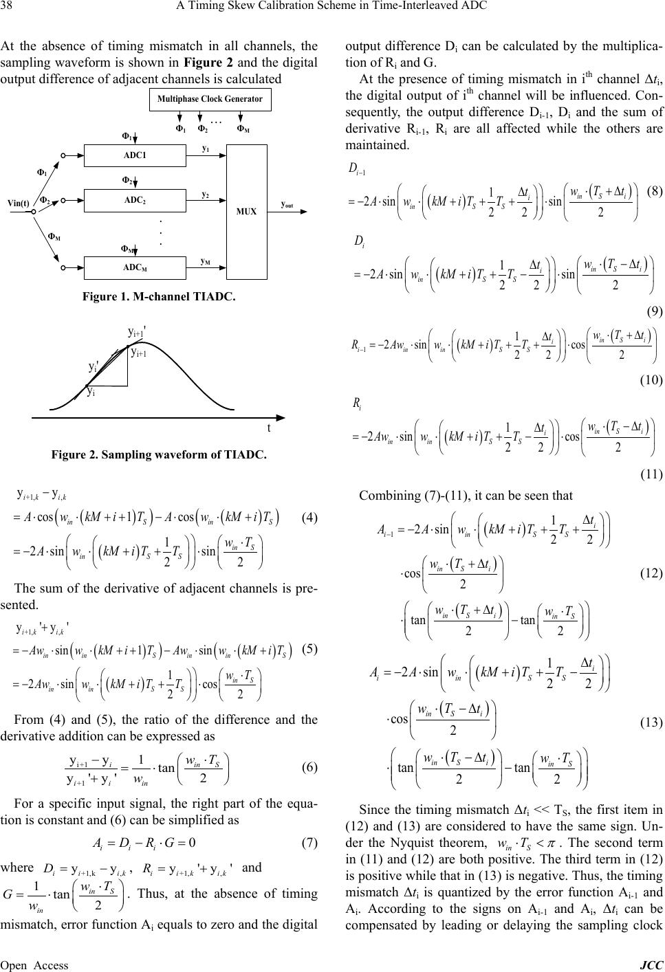 A Timing Skew Calibration Scheme in Time-Interleaved ADC Open Access JCC 38 At the absence of timing mismatch in all channels, the sampling waveform is shown in Figure 2 and the digital output difference of adjacent channels is calculated ADC1 ADC 2 ADC M . . . Vin(t) MUX y out Multiphase Clock Generator Ф 1 Ф 2 Ф M . . . Ф 1 Ф 2 Ф M Ф 1 Ф 2 Ф M y 1 y 2 y M Figure 1. M-channel TIA DC. t y i y i+1 y i+1 ' y i ' Figure 2. Sampling waveform of TIADC. ( ) ( ) ( ) ( ) ( ) +1, , yy cos1 cos 1 2 sinsin 22 i kik inSin S in S inS S AwkM iTAwkM iT T AkM iTw w T − =⋅++−⋅+ =−⋅+ +⋅ ⋅ ⋅ ⋅ ⋅ (4) The sum of the derivative of adjacent channels is pre- sented. ( ) ( ) ( ) ( ) ( ) +1, , y'y ' sin1 sin 1 2 sincos 22 i kik ininS ininS in S ininS S AwwkM iTAwwkM iT T AwkMi TTw w + =−⋅++−⋅+ =−⋅ + ⋅⋅ ⋅ ⋅+⋅ (5) From (4) and (5), the ratio of the difference and the derivative addition can be expressed as i+1 +1 yy 1tan y' y'2 iin S ii in Tw w − =⋅ + ⋅ (6 ) For a specific input signal, the right part of the equa- tion is constant and (6) can be simplified as 0 i ii ADRG= −⋅= (7) where +1,k , yy i iik D= − , +1, , y'y' ii kik R= + and 1tan 2 in S in T w w G = ⋅⋅ . Thus, at the absence of timing mismatch, error function Ai equals to zero and the digital output difference Di can be calculated by the multiplica- tion of Ri and G. At the presence of timing mismatch in ith channel Δti, the digital output of ith channel will be influenced. Con- sequently, the output difference Di-1, Di and the sum of derivative Ri-1, Ri are all affected while the others are maintained. ( )( ) 1 1 2 sinsin 222 i in S in i Si S D T AkMiTwt t w T − + =−⋅+ + +⋅ ∆ ⋅ ∆ ⋅ (8) ( )() 1 2 sinsin 222 i i in S inSS i D T AkM iwt t TTw− =−⋅+ + −⋅ ⋅∆ ∆ ⋅ (9) ( )( ) 1 2 1 2 sincos 22 in S iininS Si i T RAwkM iwt t wTT − ⋅ +∆ ∆ ⋅+ =− ⋅++⋅ (10) ( )( ) 1 2 sincos 222 i in S in ii i n SS R T AkM iwt t ww TT − =− ⋅++−⋅ ∆ ⋅ ∆ ⋅ (11) Combi ni ng (7)-(11), it can be seen that ( ) ( ) ( ) 11 2 sin2 cos 2 tan tan 2 22 i iinS S in S in Sin S i i AAkMi TT T T t w wt wt w T − ∆ ⋅+ ⋅ +∆ =−⋅+ + ⋅ ⋅− ⋅+ ⋅ ∆ (12) ( ) ( ) ( ) 1 2 sin2 cos 2 tan tan 2 2 2 iinS S in S in Sin i i iS t w wt AAkMi TT T wt w TT ∆ ⋅− ⋅ −∆ ⋅ −∆ =−⋅+ + ⋅ ⋅− ⋅ (13) Since the timing mismatch Δti << TS, the first item in (12) and (13) are considered to have the same sign. Un- der the Nyquist theorem, in S wT π ⋅< . The second term in (11) and (12) are both positive. The third term in (12) is positive while that in (1 3) is n egative. Thus, the timing mismatch Δti is quantized by the error function Ai-1 and Ai. According to the signs on Ai-1 and Ai, Δti can be compensated by leading or delaying the sampling clock 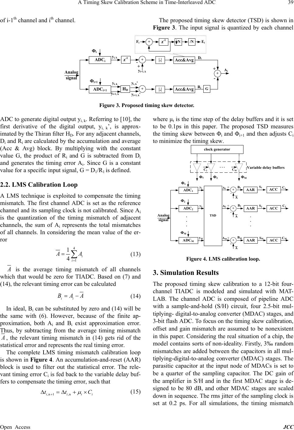 A Timing Skew Calibration Scheme in Time-Interleaved ADC Open Access JCC 39 of i-1th channel and ith channel. The proposed timing skew detector (TSD) is shown in Figure 3. The input signal is quantized by each channel ADCi ADCi+1 Analog signal Фi Фi+1 y i, k y i+1, k z-1 + - + + |.| Acc&Avg |.| Acc&Avg + z-1 N /N HD F i E i y i, k y i, k ' y i+1, k ' y i+1, k + + G A i - D i R i Figure 3. Proposed timing skew detector. ADC to generate digital output yi, k. Referring to [10], the first derivative of the digital output, yi, k’, is approx- imated by the Thiran filter HD. For any adjacent channels, Di and Ri are calculated by the accumulation and average (Acc & Avg) block. By multiplying with the constant value G, the product of Ri and G is subtracted from Di and generates the timing error Ai. Since G is a constant value for a specific input signal, G = D1/R1 is defined. 2.2. LMS Calibration Loop A LMS technique is exploited to compensate the timing mismatch. The first channel ADC is set as the reference channel and its sampling clock is not calibrated. Since Ai is the quantization of the timing mismatch of adjacent channels, the sum of Ai represents the total mismatches of all channels. In considering the mean value of the er- ror 4 1 1 4 i i AA = = ∑ (13) A is the average timing mismatch of all channels which that would be zero for TIADC. Based on (7) and (14), the relevant timing error can be calculated ii B AA= − (14) In ideal, Bi can be substituted by zero and (14) will be the same with (6). However, because of the finite ap- proximation, both Ai and Bi exist approximation error. Thus, by subtracting from the average timing mismatch A , the relevant timing mismatch in (14) gets rid of the statistical error and represents the real timing error. The complete LMS timing mismatch calibration loop is shown in Figure 4. An accumulation-and-reset (AAR) block is used to filter out the statistical error. The rele- vant timing error Ci is fed back to the variable delay buf- fers to compensate the timing error, such that ,n 1,nii ti tt C µ + ∆ =∆+× (15) where μt is the time step of the delay buffers and it is se t to be 0.1ps in this paper. The proposed TSD measures the timing skew between Φi and Φi+1 and then adjusts Ci to minimize the timing skew. ADC 1 ADC 2 ADC M Analog signal Φ 1 Φ 2 Φ M y 1 y 2 y M A M A 1 A 2 TSD + + + + AAR C M AAR C 1 C 2 + A + -AAR clock generator Φ M Φ 2 A - A - Φ 1 C 2 C M ACC ACC B M B 1 B 2 S M S 1 S 2 ACC Variable delay buffers . . . . . . . . . Figure 4. LMS calibration loop. 3. Simulation Results The proposed timing skew calibration to a 12-bit four- channel TIADC is modeled and simulated with MAT- LAB. The channel ADC is composed of pipeline ADC with a sample-and-hold (S/H) circuit, four 2.5-bit mul- tiplying- digital-to-analog converter (MDAC) stages, and 3-bit flash ADC. To focus on the timing skew calibration, offset and gain mismatch are assumed to be nonexistent in this paper. Considering the real situation of a chip, the model contains sorts of non-ideality. Firstly, 3‰ random mismatches are added between the capacitors in all mul- tiplying-digital-to-analog converter (MDAC) stages. The parasitic capacitor at the input node of MDACs is set to be a quarter of the sampling capacitor. The DC gain of the amplifier in S/H and in the first MDAC stage is de- signed to be 80 dB, and other MDAC stages are scaled down in sequence. The rms jitter of the sampling clock is set at 0.2 ps. For all simulations, the timing mismatch 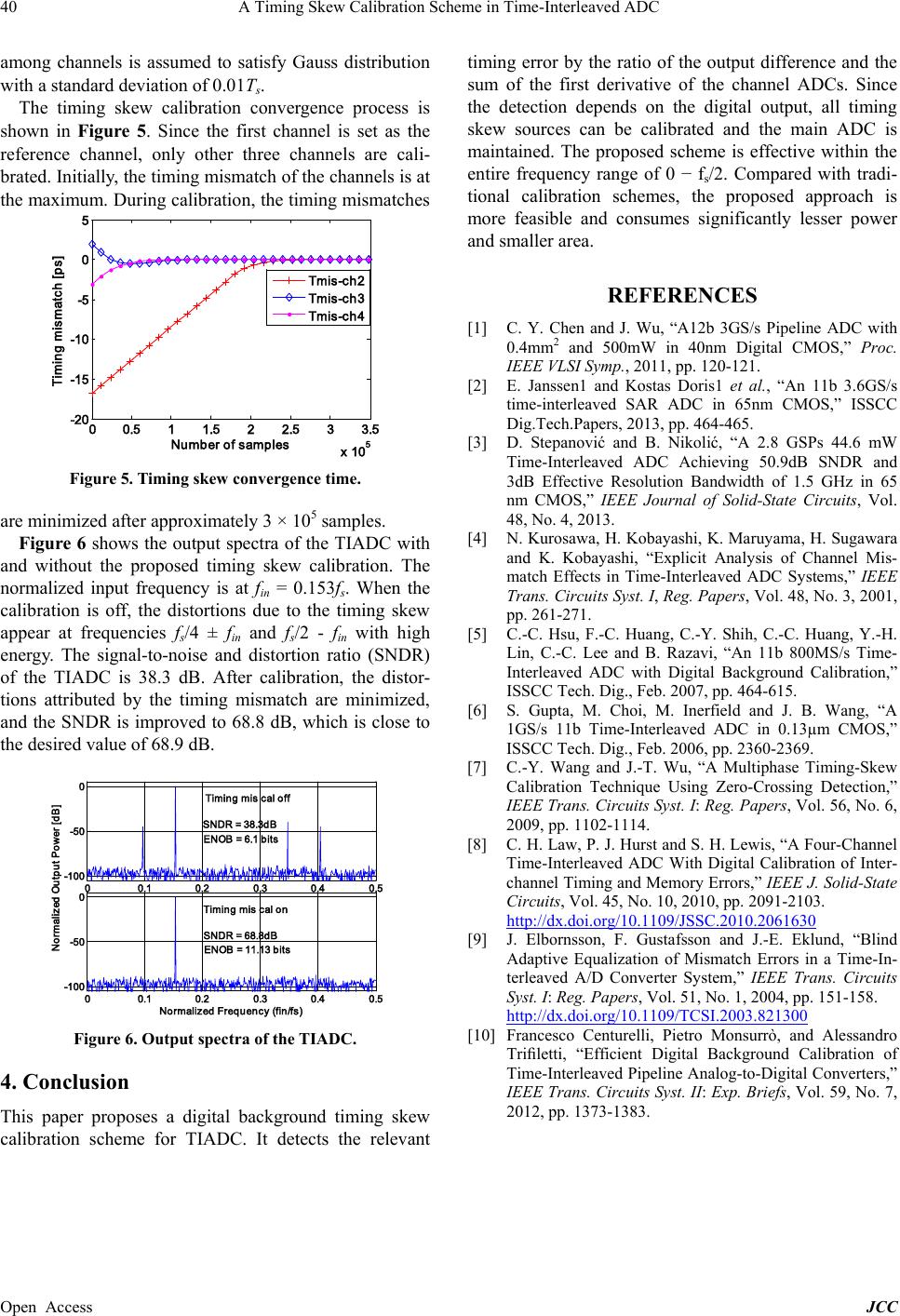 A Timing Skew Calibration Scheme in Time-Interleaved ADC Open Access JCC 40 among channels is assumed to satisfy Gauss distribution with a sta n da rd devia t ion of 0.01Ts. The timing skew calibration convergence process is shown in Figure 5. Since the first channel is set as the reference channel, only other three channels are cali- brated. Initially, the timing mismatch of the channels is at the maximum. During calibration , the timing mismatches Figure 5. Timing skew convergence time. are minimized after approximately 3 × 10⁵ samp le s. Figure 6 shows the output spectra of the TIADC with and without the proposed timing skew calibration. The normalized input frequency is at fin = 0.153fs. When the calibration is off, the distortions due to the timing skew appear at frequencies fs/4 ± fin and fs/2 - fin with high energy. The signal-to-noise and distortion ratio (SNDR) of the TIADC is 38.3 dB. After calibration, the distor- tions attributed by the timing mismatch are minimized, and the SNDR is improved to 68.8 dB, which is close to the desired value of 68.9 dB. Figure 6. Output spectra of the TIADC. 4. Conclusion This paper proposes a digital background timing skew calibration scheme for TIADC. It detects the relevant timing error by the ratio of the output difference and the sum of the first derivative of the channel ADCs. Since the detection depends on the digital output, all timing skew sources can be calibrated and the main ADC is maintained. The proposed scheme is effective within the entire frequency range of 0 − fs/2. Compared with tradi- tional calibration schemes, the proposed approach is more feasible and consumes significantly lesser power and smaller area. REFERENCES [1] C. Y. Chen and J. Wu, “A12b 3GS/s Pipeline ADC with 0.4mm2 and 500mW in 40nm Digital CMOS,” Proc. IEEE VLSI Symp., 2011, pp. 120-121. [2] E. Janssen1 and Kostas Doris1 et al., “An 11b 3.6GS/s time-interleaved SAR ADC in 65nm CMOS,” ISSCC Dig.Tech.Papers, 2013, pp. 464-465. [3] D. Stepanović and B. Nikolić, “A 2.8 GSPs 44.6 mW Time-Interleaved ADC Achieving 50.9dB SNDR and 3dB Effective Resolution Bandwidth of 1.5 GHz in 65 nm CMOS,” IEEE Journal of Solid-State Circuits, Vol. 48, No. 4, 2013. [4] N. Kuros awa, H. Kobayashi, K. Maruyama, H. Sugawara and K. Kobayashi, “Explicit Analysis of Channel Mis- match Effects in Time-Interleaved ADC Systems,” IEEE Trans. Circuit s Syst. I, Reg. Papers, Vol. 48, No. 3, 2001, pp. 261-271. [5] C.-C. Hsu, F.-C. Huang, C.-Y. Shih, C.-C. Huang, Y.-H. Lin, C.-C. Lee and B. Razavi, “An 11b 800MS/s Time- Interleaved ADC with Digital Background Calibration,” ISSCC Tech. Dig., Feb. 2007, pp. 464-615. [6] S. Gupta, M. Choi, M. Inerfield and J. B. Wang, “A 1GS/s 11b Time-Interleaved ADC in 0.13µm CMOS,” ISSCC Tech. Dig., Feb. 2006, pp. 2360-2369. [7] C.-Y. Wang and J.-T. Wu, “A Multiphase Timing-Skew Calibration Technique Using Zero-Crossing Detection,” IEEE Trans. Circuits Syst. I: Reg. Papers, Vol. 56, No. 6, 2009, pp. 1102-1114. [8] C. H. Law, P. J. Hurst and S. H. Le wis, “A Four-Channel Time-Interleaved ADC With Digital Calibration of Inter- channel Timing and Memory Errors,” IEEE J. Solid-State Circuits, Vol. 45, No. 10, 2010, pp. 2091-2103. http://dx.doi.org/10.1109/JSSC.2010.2061630 [9] J. Elbornsson, F. Gustafsson and J.-E. Eklund, “Blind Adaptive Equalization of Mismatch Errors in a Time-In- terleaved A/D Converter System,” IEEE Trans. Circuits Syst. I: Reg. Papers, Vol. 51, No. 1, 2004, pp. 151-158. http://dx.doi.org/10.1109/TCSI.2003.821300 [10] Francesco Centurelli, Pietro Monsurrò, and Alessandro Trifiletti, “Efficient Digital Background Calibration of Time-Interleaved Pipeline Analog-to-Digital Converters,” IEEE Trans. Circuits Syst. II: Exp. Briefs, Vol. 59, No. 7, 2012, pp. 1373-1383. 00.5 11.5 22.5 33.5 x 10 5 -20 -15 -10 -5 0 5 N um ber of sampl es T im ing m isma tc h [ ps] Tmis-ch2 Tmis-ch3 Tmis-ch4 00.1 0.2 0.3 0.4 0.5 -100 -50 0Timing mis cal off SNDR = 38.3dB ENOB = 6.1 bits 00.1 0.2 0.3 0.4 0.5 -100 -50 0 Nor m ali zed Fre quency (fi n/fs) Nor m alized Output Power [dB] Timing mis cal on SNDR = 68.8dB ENOB = 11.13 bits |