

Paper Menu >>
Journal Menu >>
 Journal of Power and Energy Engineering, 2013, 1, 1-6 http://dx.doi.org/10.4236/jpee.2013.15001 Published Online October 2013 (http://www.scirp.org/journal/jpee) Copyright © 2013 SciRes. JPEE 1 New Multilevel Mixed Topology Development to Improve Inverter Robustness for Domestic Photovoltaic Installations Sébastien Jacqu es, Adelp he Caldeira, Ambroise Schellmanns, Zheng Ren, Nathalie Batut GREMAN UMR-CNRS 7347, University of Tours, 7 Avenue Marcel Dassault, 37200 Tours, France. Email: [email protected] Received July 2013 ABSTRACT Multilevel inverters are well u sed in grid connected domestic p hotovoltaic applications because of their ability to gen- erate a very good quality of waveforms, reducing switching frequency, and their low voltage stress across the power devices. However, this kind of inverter has to be modified to both limit common-mode currents and improve the ro- bustness of the system. This paper presents a new mixed 5-level inv erter that meets these challenges. The op erating principle of the converter is proposed. Several experimental measurements are described to validate this new concept. The output voltage and current and the THD of the output voltage are particularly discussed. Keywords: Domestic PV Applications; Common Mode Currents; Decoupling Capacitances; Mixed 5-Level Inverter 1. Introduction The global market for solar photovoltaic (PV) systems using tran sformerless config ur a tion has been growing over the last decade or more with an average rate from 30% to 40% per year. In particular, grid-connected PV installations contribute significantly to this a verage growth rate [1]. The technical performances and robustness of inverters are key elements t hat may have a significant impact on the generation of electricity and the profitabil- ity of domestic grid-con nected PV systems. PV inverters typically operate with a switching fre- quency of about 15 kHz. As can be seen in F igure 1, this frequency can be reflected to the DC bus and gener ate common-mode currents which flow through the metallic frame and the stray capacitances of the PV modules [2,3]. These parasitic capacitances are key contributors of a resonant circuit which consists of the PV modules, the AC filter elements and the grid impedance. The value of these str ay capacitances, which could reach 1 50 nF∙kW−1, depends on weather conditions, PV topology, PWM pat- tern, the material used in the metallic frame and the pas- sive elements of the converters [4]. The transformerless configura tion for PV systems could result in safety prob- lems particularly when leakage currents appear at th e positiv e and negative PV terminals. Th e DIN VDE 0126-1-1 document specifies that the maximum leakage ground current is equal to 300 mA [5]. Regarding do- mestic applications, the UTE C 15-712 standa rd requires the use of 30 mA differential circ uit breaker inside the PV installation. However, the leakage current can in- crease over 30 mA that lead s to the installation shutting down. So, the limitation of common-mode currents has become an important challenge. NPC (Neutral Point Clamping) topologies are well- known converter structures that are able to eliminate common-mode currents because the middle point of the DC source is fixed (i.e. clamped by diodes). Therefore, no leakage current can be generated [6,7]. In symmetrical configura tion, 5-level NPC inverter enables to signifi- cantly improve the Total Harmonic Distortion (THD) of the output voltage and current and decrease the voltage constraints across the semiconductor devices in compar- ison with the H-bridge converter topology. However, 5- level NPC inverter requires the use of 4 decoupling ca- pacitors, 8 power switches and 6 clamping diodes that could considerably increase the complexity and cost- effectiveness of the system. It is important to notice that the electrolytic capacitors, u sed for power decoupling between and the single-phase grid, are the main limiting components inside the inverter. Equation (1) shows that the operational lifetime (LOP) of the decoupling capacitor depends on the hotspot temperature (Th). The LOP,0-pa- rameter is the lifetime at a hotspot temperature of T0. The ∆T-parameter is the temperature increase that reduces the lifetime by a factor of two [8]. 0h – T (T )/DT OP OP,0 LL 2= × (1 ) 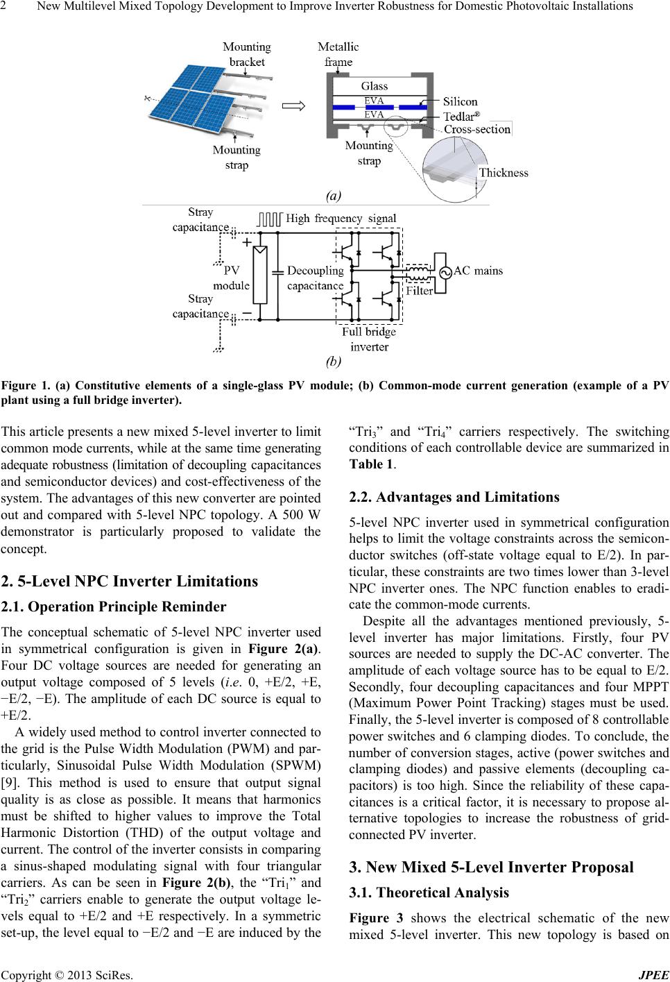 New Multilevel Mixed Topology Development to Improve Inverter Robustness for Domestic Photovoltaic Installations Copyright © 2013 SciRes. JPEE 2 Figure 1. (a) Constitutive elements of a single-glass PV module; (b) Common-mode current generation (example of a PV plant using a full bridge inverter). This article pr esents a new mixed 5-level inverter to limit common mode currents, while at the same time generating adequate robustness (limitation of decoupling capacitances and semiconductor devices) and cost-effectiveness of the system. The adv antages of this new conver ter are pointed out and compared with 5-level NPC topology. A 500 W demonstrator is particularly proposed to validate the concept. 2. 5-Level NPC Inverter Limitations 2.1. Operation Principle Reminder The conceptual schematic of 5-lev el NPC inverter used in symmetrica l configuration is given in Figure 2(a). Four DC voltage sources are needed for gen erating an output voltage composed of 5 levels (i.e. 0, +E/2, +E, −E/2, −E). The amplitude of each DC source is equal to +E/2. A widely used method to control inverter connec ted to the grid is the Pulse Width Modulation (PWM) and par- ticularly, Sinusoidal Pulse W idth Modulation ( SPWM) [9]. This method is used to ensure that output signal quality is as close as possible. It means that harmonics must be shifted to higher values to improve the Total Harmonic Distortion (THD) of the output voltage and current. The control of the inverter consists in comparing a sinus-sh aped modulating signal with four triangular carriers. As can be seen in Figure 2(b), the “Tri1” and “Tri2” carriers enable to generate the output voltage le- vels equal to +E/2 and +E respectively. In a symmetric set-up, the level equal to −E/2 and −E are induced by the “Tri3” and “Tri4” carriers respectively. The switching conditions of each controllable device are summarized in Table 1. 2.2. Advantages and Limitations 5-leve l NPC inverter used in symmetrical configur ation helps to limit the voltage constraints across the semicon- ductor switches (off-state voltage equal to E/2). In par- ticular, th ese constraints are two times lower t han 3-l evel NPC inverter ones. The NPC function enables to eradi- cate the common-mode currents . Despite all the advantages mentioned previously, 5- level inverter has major limitations. Firstly, f ou r PV sources are needed to supply the DC-AC converter. The amplitude of each voltage source has to be equal to E/2. Secondly, four decoupling capacitances and four MPPT (Maximum Power Point Tracking) stages must be used. Finally, the 5-level inverter is composed of 8 controllable power switches and 6 clamping diodes. To conclude, the number of conversion stages, active (power switches and clamping diodes) and passive elements (decoupling ca- pacitors) is too high. Since the reliability of these capa- citances is a critical factor, it is necessary to propose al- ternative topologies to increase the robustness of grid- connected PV inverter. 3. New Mixed 5-Level Inverter Proposal 3.1. Theoretical Analysis Figure 3 shows the electrical schematic of the new mixed 5-level inverter. This new topology is based on 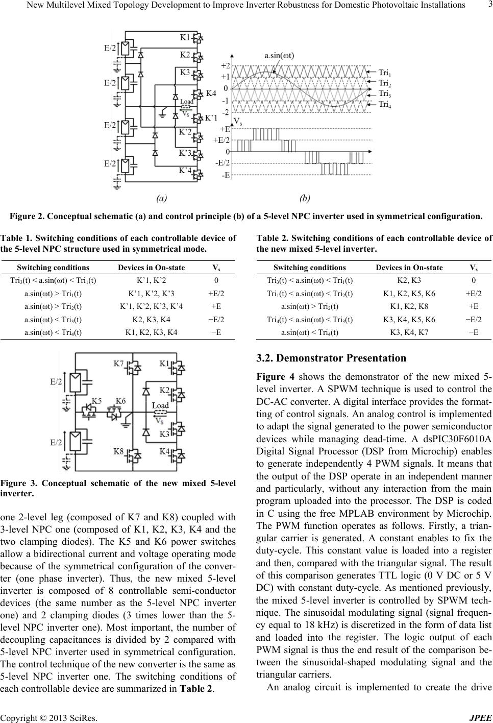 New Multilevel Mixed Topology Development to Improve Inverter Robustness for Domestic Photovoltaic Installations Copyright © 2013 SciRes. JPEE 3 Figure 2. Conceptual schematic (a) and control principle (b) of a 5-leve l NPC inverter used in symmetrical confi guration. Table 1. Switching conditions of each controllable device of the 5-level NPC structure used in symmetrical mode. Switching conditions Devices in On-state Vs Tri3(t) < a.sin(ωt) < Tri1(t) K’1, K’2 0 a.sin(ωt) > Tri1(t) K’1, K’2, K’3 +E/2 a.sin(ωt) > Tri2(t) K’1, K’2, K’3, K’4 +E a.sin(ωt) < Tri3(t) K2, K3, K4 −E/2 a.sin(ωt) < Tri4(t) K1, K2, K3, K4 −E Figure 3. Conceptual schematic of the new mixed 5-level inverter. one 2-level leg (composed of K7 and K8) coupled with 3-leve l NPC one (composed of K1, K2, K3, K4 and the two clamping diodes). The K5 and K6 power switches allow a bidirectional current and voltage operating mode because of the symmetrical co nfiguration of the conver- ter (one phase inverter). Thus, the new mixed 5-level inverter is composed of 8 controllable semi-conductor devices (the same number as the 5-level NPC inve rter one) and 2 clamping diodes (3 times low er than the 5- level NPC inverter one). Most important, the number of decoupling capacitances is divided by 2 compared with 5-leve l NPC inverter used in symmetrical configuration. The control technique of the new converte r is the same as 5-leve l NPC inverter one. The switching conditions of each controllable device are summarized in Table 2. Table 2. Switching conditions of each controllable device of the new mixed 5-l evel inverter. Switching conditions Devices in On-state Vs Tri3(t) < a.sin(ωt) < Tri1(t) K2, K3 0 Tri1(t) < a.sin(ωt) < Tri2(t) K1, K2, K5, K6 +E/2 a.sin(ωt) > Tri2(t) K1, K2, K8 +E Tri4(t) < a.sin(ωt) < Tri3(t) K3, K4, K5, K6 −E/2 a.sin(ωt) < Tri4(t) K3, K4, K7 −E 3.2. Demonstrator Presentation Figure 4 shows the demonstrator of the new mixed 5- level inverter. A SPWM technique is used to control the DC-AC converter. A digital interface provides the format- ting of control signals. An analog control is implemented to adapt the signal generated to the power semiconductor devices while managing de ad-time. A dsPI C30F6010A Digital Signal Processor (DSP from Microchip) enables to generate independently 4 PWM signals. It means that the output of the DSP operate in an independent manner and particularly, without an y interaction from the main program uploaded into the processor. The DSP is coded in C using the free MPLAB environment by Microchip. The PW M function operates as follows. Firstly, a trian- gular carrier is generated. A constant enables to fix the duty-cycle. This constant value is loaded into a register and then, compa red with the triangular signal. The result of this comparison generates TTL logic (0 V DC or 5 V DC) with constant duty-cycle. As mentioned previously, the mixed 5-level inverter is controlled by SPWM tech- nique. The sinusoidal modulating signal (signal frequen- cy equal to 18 kHz) is discretized in the form of data list and loaded into the register. The logic output of each PWM signal is thus the end result of the comparison be- tween the sinusoidal-shaped modulating signal and the triangular carriers. An analog circuit is implemented to create the drive 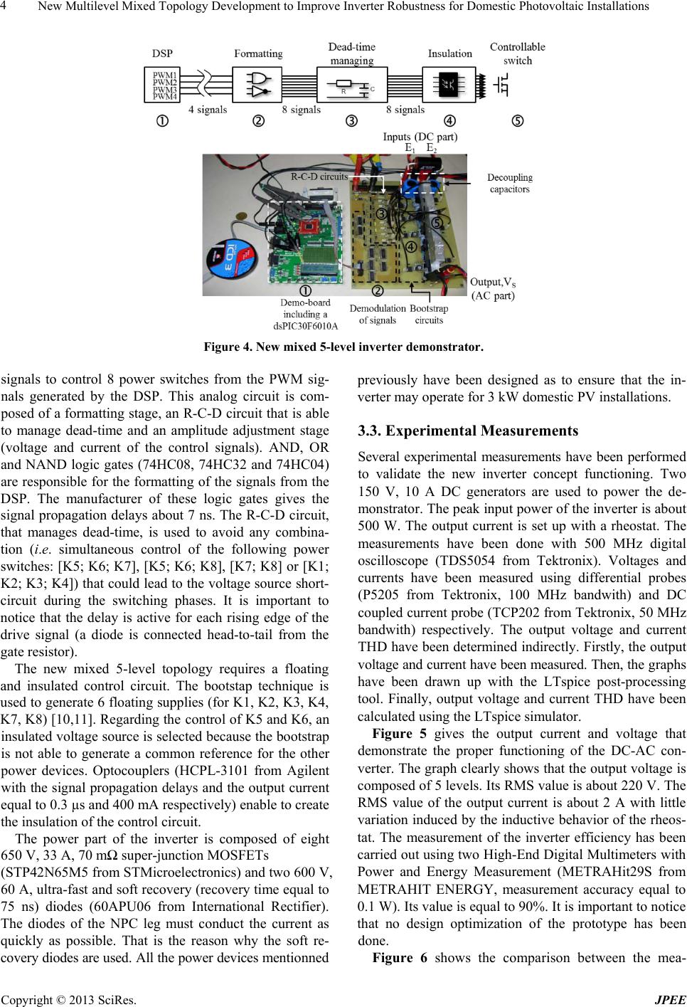 New Multilevel Mixed Topology Development to Improve Inverter Robustness for Domestic Photovoltaic Installations Copyright © 2013 SciRes. JPEE 4 Figure 4. New mixed 5-level inverter demonstrator. signals to control 8 power switches from the PWM sig- nals generated by the DSP. This analog circuit is com- posed of a formatting stage, an R-C-D circuit that is able to manage dead-time and an amplitude adjustment stage (voltage and current of the control signals). AND, OR and NAND logic gates (74HC08, 74H C32 and 74HC04) are responsible for the formatting of the signals from the DSP. The manufacturer of these logic gates gives the signal propagation delays about 7 ns. The R-C-D circuit, that manages dead-time, is used to avoid any combina- tion (i.e. simultaneous control of the following power switches: [K5; K6; K7], [K5; K6; K8], [K7; K8] or [K1; K2; K3; K4]) that could lead to the voltage source short- circuit during the switching phases. It is important to notice that the delay is active for each rising edg e of the drive signal (a diode is connected head-to-tail from the gate resistor). The new mixed 5-level topology requires a floating and insulated control circuit. The bootstap technique is used to generate 6 floating supplies (for K1, K2, K3, K 4, K7, K8) [10,11]. Regarding the control of K5 and K6, an insulated voltage source is selected because the bootstrap is not able to generate a common reference for the other power devices. Optocouplers (HCPL-3101 from Agilent with the signal propagation delays and the output current equal to 0.3 µs and 400 mA respectively) en able to create the insulation of the control circuit. The power part of the inverter is composed of eight 650 V, 33 A, 70 mΩ super-junction MOSFETs (STP42N65M5 from STMicroelectronics) and two 600 V, 60 A, ultra-fast an d soft recover y (recovery time equal to 75 ns) diodes (60APU06 from International Rectifier). The diodes of the NPC leg must conduct the current as quickly as possible. That is the reason why the soft re- covery diodes are used. All the power devices mentionned previously have been designed as to ensure that the in- verter may operate for 3 kW domestic PV installations. 3.3. Experimental Measurement s Several experimental measurements have been performed to validate the new inverter concept functioning. Two 150 V, 10 A DC generators are used to power the de- monstrator. The peak input power of the inverter is about 500 W. The outpu t current is set up with a rheostat. The measurements have been done with 500 MHz digital oscilloscope (TDS5054 from Tektronix). Voltages and currents have been measured using differential probes (P5205 from Tektronix, 100 MHz bandwith) and DC coupled current probe (TCP202 fro m Tektronix, 50 MHz bandwith) respectively. The output voltage and current THD have been determined indirectly. Firstly, the output voltage and current have been measured. Then, the graphs have been drawn up with the LTspice post-processing tool. Finally, output voltage and current THD have been calculated using the LTspice simulator. Figure 5 gives the output current and voltage that demonstrate the proper functioning of the DC-AC con- verter. The graph clearly shows that the output voltage is composed of 5 levels. Its RMS value is about 220 V. The RMS value of the output current is about 2 A with little variation induced by the inductive behavior of the rheos- tat. The measurement of the inverter efficiency has been carried out using two High-End Digital Multimeters with Power and Ene rgy Measurement (METRAHit29S from METRAHIT ENERGY, measurement accuracy equal to 0.1 W). Its value is equal to 90%. It is important to notice that no design optimization of the prototype has been done. Figure 6 shows the comparison between the mea- 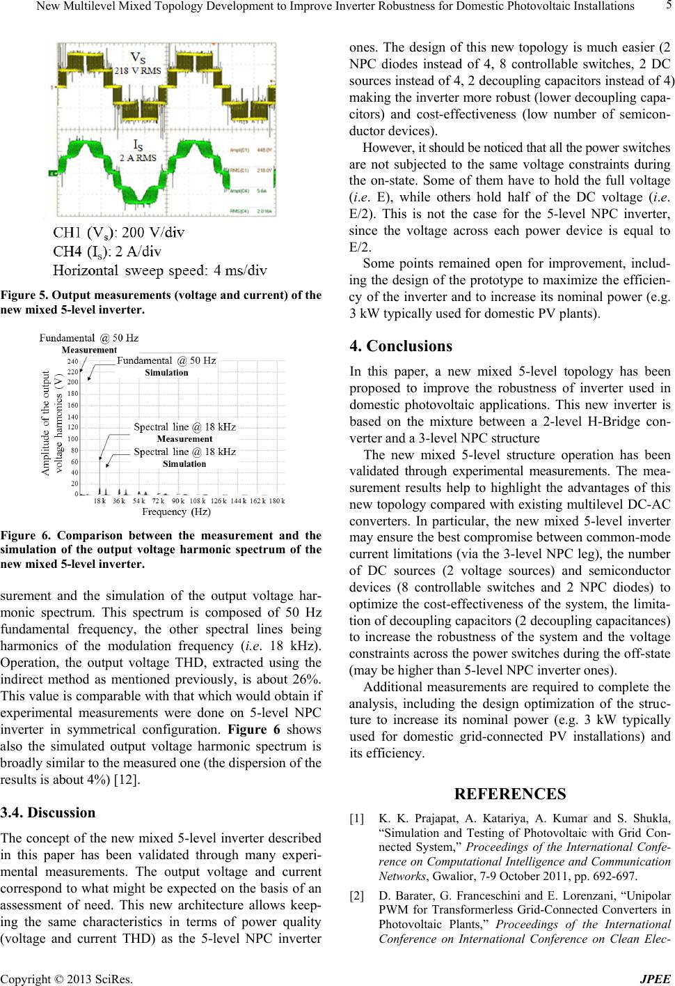 New Multilevel Mixed Topology Development to Improve Inverter Robustness for Domestic Photovoltaic Installations Copyright © 2013 SciRes. JPEE 5 Figure 5. Output measurements (voltage and current) of the new mixed 5 -level inverter. Figure 6. Comparison between the measurement and the simulation of the output voltage harmonic spectrum of the new mixed 5 -level inverter. surement and the simulation of the output voltage har- monic spectrum. This spectrum is composed of 50 Hz fundamental frequency, the other spectral lines being harmonics of the modulation frequency (i.e. 18 kHz ). Operation, the output voltage THD, ext racted using the indirect method as mentioned previously, is about 26%. This value is comparable with that which would obtain if experimental measurements were done on 5-level NPC inverter in symmetrical conf iguration. Figure 6 shows also the simulated output voltage harmonic spectrum is broadly similar to the measured one (the dis pe r s ion of the results is about 4%) [12]. 3.4. Discussion The concept of the new mixed 5-level inverter descri bed in this paper has been validated through many experi- mental measurements. The output voltage and current correspond to what might be expected on the basis of an assessment of need. This new architecture allows keep- ing the same characteristics in terms of power quality (voltage and current THD) as the 5-level NPC inverter ones. The design of this new topology is much easier (2 NPC diodes instead of 4, 8 controllable switches, 2 DC sources instead of 4, 2 decoupling capacitors instead of 4) making the inverter more robust (lower decoupling capa- citors) and cost-effectiveness (low number of semicon- ductor devices). However, it should be noticed that all the power switches are not subjected to the same voltage constraints during the on-state. Some of them have to hold the full voltage (i.e. E), while others hold half of the DC voltage (i.e. E/2). This is not the case for the 5-level NPC inve rter, since the voltage across each power device is equal to E/2. Some points remained open for improvement, includ- ing the design of the prototype to maximize the efficien- cy of the inverter and to increase its nominal power (e.g. 3 kW typically used for domestic PV plants). 4. Conclusions In this paper, a new mixed 5-level topology has been proposed to improve the robustness of inverter used in domestic photovoltaic applications . Th is new inverter is based on the mixture between a 2-level H-Bridge con- verter and a 3-level NPC structure The new mixed 5-level structure operation has be en validated through experimental measurements. The mea- surement results help to highlight the advantages of this new topology compared with existing multilevel DC-AC converters. In particular, the new mixed 5-level inverter may ensure the best compromise between common-mode current limitations (via the 3-level NPC leg), the number of DC sources (2 voltage sources) and semiconductor devices (8 controllable switches and 2 NPC diodes) to optimize the cost-effectiveness of the system, the limita- tion of decoupling capacitors (2 decoupling capacitances) to increase the robustness of the system and the voltage constraints across the pow er switches d uring the off-state (may be higher than 5-level NPC inverter ones). Additional measurements are r equired to complete the analysis, including the design optimization of the struc- ture to increase its nominal power (e.g. 3 kW typically used for domestic grid-connected PV installations) and its efficiency. REFERENCES [1] K. K. Prajapat, A. Katariya, A. Kumar and S. Shukla, “Simulation and Testing of Photovoltaic with Grid Con- nected System, ” Proceedings of the International Confe- rence on Computational Intelligence and Communication Networks, Gwalior, 7-9 October 2011, pp. 692-697. [2] D. Barater, G. Franceschini and E. Lorenzani, “Unipolar PWM for Transformerless Grid-Connected Converters in Photovoltaic Plants,” Proceedings of the International Conference on International Conference on Clean Elec-  New Multilevel Mixed Topology Development to Improve Inverter Robustness for Domestic Photovoltaic Installations Copyright © 2013 SciRes. JPEE 6 trical Power, 2009, pp. 387-392. [3] G. Vazquez, T. Kerekes, J. Rocabert, P. Rodriguez, R. Teodorescu and D. Aguilar, “A Photovoltaic Three-Phase Topology to Reduce Common Mode Voltage,” Proceed- ings of the IEEE International Symposium on Industrial Electronics, 2010, pp. 2885-2890. [4] T. Kerekes, R. Teodorescu, and U. Borup, “Transformer- less Photovoltaic Inverters Connected to the Grid,” Pro- ceedings of the IEEE Applied Power Electronics Confe- rence, 2007, pp. 1733-1737. [5] DKE Deutsche Kommission Elektrotechnik Elektronik In- formations Technik im DIN und VDE, DIN VDE 0126- 1-1, 2005. [6] Y. Cheng, C. Qian, M. L. Crow and S. Pekarek, “A Comparison of Diode-Clamped and Cascaded Multilevel Converters for a STATCOM with Energy Storage,” IEEE Transactions on Industrial Electronics, Vol. 53, No. 5, 2006, pp. 1512-1521. http://dx.doi.org/10.1109/TIE.2006.882022 [7] M. Baldé, M. Lamine Doumbia, A. Chériti and C. Bena- chaiba, “Comparative Study of NPC and Cascaded Con- verters Topologies,” Renewable Energy and Power Qual- ity Journal, No. 9, 2011. [8] S. B. Kjaer, J. K. Pedersen and F. Blaabjerg, “A Review of Single-Phase Grid-Connected Inverters for Photovol- taic Modules,” IEEE Transactions on Industry Applica- tions, Vol. 41, No. 5, 2005, pp. 1292-1306. http://dx.doi.org/10.1109/TIA.2005.853371 [9] P. K. Chaturvedi, S. Jain and P. Agarwal, “Reduced Switching Loss Pulse Width Modulation Technique for Three-Level Diode Clamped Inverter,” IET Power Elec- tronics, Vol. 4, No. 4, 2011, pp. 393-399. http://dx.doi.org/10.1049/iet-pel.2010.0311 [10] S. S. Dash, P. Palanivel and S. Premalatha, “Performance Analysis of Multilevel Inverters Using Variable Switch- ing Frequency Carrier Based PWM Techniques,” Re- newable Energy and Power Quality Journal, No. 10, 2012. [11] T. Suroso, “Common-Emitter Topology of Multilevel Cur- rent-Source Pulse Width Modulation Inverter with Chop- per-Based dc Current Sources,” IET Power Electronics, Vol. 4, No. 7, 2011, pp. 759-766. http://dx.doi.org/10.1049/iet-pel.2010.0008 [12] A. Caldeira, S. Jacques, A. Schellmanns, J.-C. Lebunetel, N. Batut and L. Gonthier, “Development of a New Mixed 5-Level Inverter for 3 kW Household Photovoltaic Ap- plications,” Renewable Energy and Power Quality Jour- nal, No. 11, 2013. [13] S. Shobana and J. PadmaPriya, “Improved H igh Effi- ciency Inverter with H6 Type Configuration to Eliminate CMLC for PV System,” International Journal of Ad- vancements in Electrical and Electronics Engineering, Vol. 2, No. 1, 2013, pp. 49-58. |