

Paper Menu >>
Journal Menu >>
 Energy and Power Engineering, 2013, 5, 1398-1403 doi:10.4236/epe.2013.54B265 Published Online July 2013 (http://www.scirp.org/journal/epe) Comparison among Chargers of Electric Vehicle Based on Different Control Strategies* Pengxin Hou, Chunlin Guo, Yubo Fan State Key Laboratory for Alternat e El ectrical Power Sy stem with Renewable E n ergy Sources, North China Electric Power University, Beijing, China Email: [email protected] Received March, 2013 ABSTRACT The charger of electric vehicle is a power electronic device which consists of rectifying de vices and DC-DC conver ters. This nonlinear diode rectifier circuit has low power factor and high harmonic content. In order to improve power factor and reduce the harmonic distortion rate of the AC side current, single-phase non-controlled rectifier charger needs to install the active power factor correction device. A piece of power system analysis software which is called PSCAD is used in modeling of an EV charger which contains Boost-APFC. By means of simulation and analysis, differences of APFC characteristics between the hysteresis current control mode and average current control mode which has an in- fluence on the power grid are compared. The consequence of simulation shows that the two control strategies achieve power factor correction and harmonic reduction requirements; Boost type power conversion circuit employs the average current control mode is better, which has following features: relatively faster settling time of the output voltage, rela- tively smaller overshoot, lower current harmonic distortion rate on AC side, lower switching frequency and better con- trol effect. Keywords: Electric Vehicle Charger; APFC; Control Strategy; Power Factor; Harmonic 1. Introduction Environmental and energy consumption problems have become the focus of the public throughout the world. Electric vehicle, as a high-speed developing transport, has an unparalleled advantage on energy conservation, and reduction in pollutant emission. As the energy supply facilities of Electric vehicle, charging station is the es- sential part in the development of electric vehicle [1]. One of the main equipments of the electric vehicle is charger that is an electrical and electronic device consisting of rectifier, DC/DC converter and etc [2]. Due to the no- nlinear structure of the charging system, a large number of harmonic current components are produced that makes harmonic noise of the circuit increase and power factor decrease. The conventional approach is to add filters at the input of the rectifier circuit, but the cost of the method is so high and the volume and weight is too large [3]. Therefore, in order to enhance the performance of the on-board charging system, active power factor correction (APFC) device need to be installed to improv e the power factor of the system input side and reduce harmonics. Aiming at low-power single-phase uncontrolled recti- fying charger, a simulation model of the Boost converter circuit is builds in this thesis with the utilization of elec- tromagnetic transient simulation tool PSCAD / EMT-DC [4], studying two different typical strategies separately used for controlling circuit, and making a comparative analysis of the input voltage and current waveforms, output voltage, AC side current harmonic distortion and etc. 2. EV Charger Simulation Model EV charger rectifier filter circuit is composed b y the rec- tifier diode and the energy storage element filter capaci- tor, and the nonlinear element leads to the conduction angle of the rectifying element less than 180 degrees. When the input peak voltage exceeds the voltage across the filter capacitor, the rectifier diode has electric current to flow through, which results in severe distortion of the input AC current waveform [5]. Figure 1 shows an AC side voltage and current waveforms, the green curve is the voltage waveform, and the blue curve is the current waveform. Current was pulse-like, which leads the input AC voltage and current to generate the additional phase shift. And the input side contains a lot of higher harmon- *This work is supported by: National High Technology R&D Program of China (863Program) (2012AA050804), Key Project of the National Research Program of China (2011BAG02B14), National High Tech- nology R&D Program of China (863 Program) (2011AA05A109). Copyright © 2013 SciRes. EPE 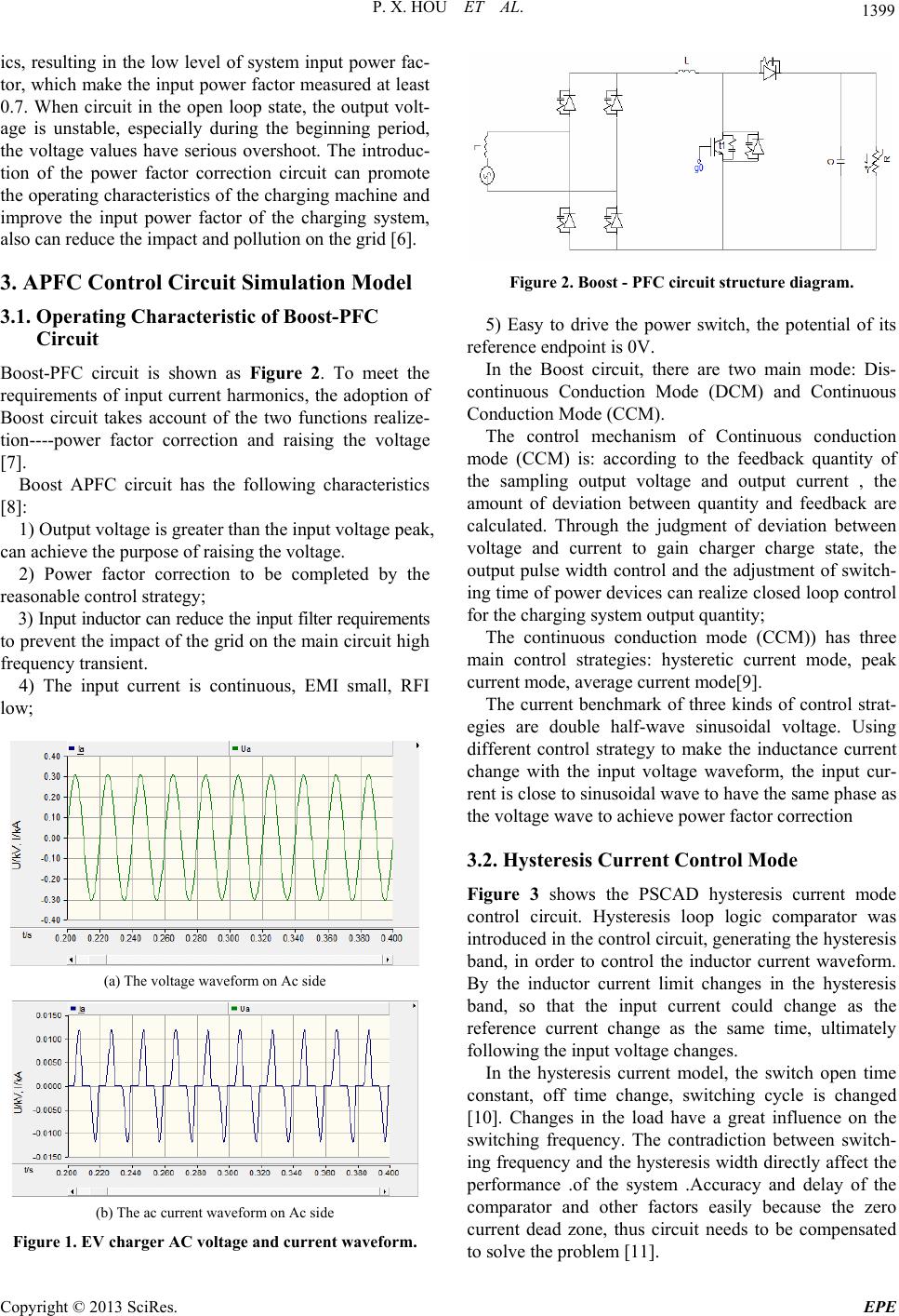 P. X. HOU ET AL. 1399 ics, resulting in the low level of system input power fac- tor, which make the input power factor measured at least 0.7. When circuit in the open loop state, the output volt- age is unstable, especially during the beginning period, the voltage values have serious overshoot. The introduc- tion of the power factor correction circuit can promote the operating characteristics of the charging machine and improve the input power factor of the charging system, also can reduce the impact and polluti o n o n t he grid [6]. 3. APFC Control Circuit Simulation Model 3.1. Operating Characteristic of Boost-PFC Circuit Boost-PFC circuit is shown as Figure 2. To meet the requirements of input current harmonics, the adoption of Boost circuit takes account of the two functions realize- tion----power factor correction and raising the voltage [7]. Boost APFC circuit has the following characteristics [8]: 1) Output voltage is greater than the input voltag e peak, can achieve the purpose of raising the voltage. 2) Power factor correction to be completed by the reasonable control strategy; 3) Input inductor can reduce the input filter requirements to prevent the impact of the grid on the main circuit high frequency transient. 4) The input current is continuous, EMI small, RFI low; (a) The voltage waveform on Ac side (b) The ac current waveform on Ac side Figure 1. EV charger AC voltage and current waveform. Figure 2. Boost - PFC circuit structure diagram. 5) Easy to drive the power switch, the potential of its reference endpoint is 0V. In the Boost circuit, there are two main mode: Dis- continuous Conduction Mode (DCM) and Continuous Conduction Mod e (CCM). The control mechanism of Continuous conduction mode (CCM) is: according to the feedback quantity of the sampling output voltage and output current , the amount of deviation between quantity and feedback are calculated. Through the judgment of deviation between voltage and current to gain charger charge state, the output pulse width control and the adjustment of switch- ing time of power devices can realize closed loop control for the charging system output quantity; The continuous conduction mode (CCM)) has three main control strategies: hysteretic current mode, peak current mode, average current mode[9]. The current benchmark of three kinds of control strat- egies are double half-wave sinusoidal voltage. Using different control strategy to make the inductance current change with the input voltage waveform, the input cur- rent is close to sinusoidal wave to have the same phase as the voltage wave to achieve power factor correction 3.2. Hysteresis Current Control Mode Figure 3 shows the PSCAD hysteresis current mode control circuit. Hysteresis loop logic comparator was introduced in the contro l circuit, g enerating the h ysteresis band, in order to control the inductor current waveform. By the inductor current limit changes in the hysteresis band, so that the input current could change as the reference current change as the same time, ultimately following the input voltage chang es. In the hysteresis current model, the switch open time constant, off time change, switching cycle is changed [10]. Changes in the load have a great influence on the switching frequency. The contradiction between switch- ing frequency and the hysteresis width directly affect the performance .of the system .Accuracy and delay of the comparator and other factors easily because the zero current dead zone, thus circuit needs to be compensated to solve the problem [11]. Copyright © 2013 SciRes. EPE 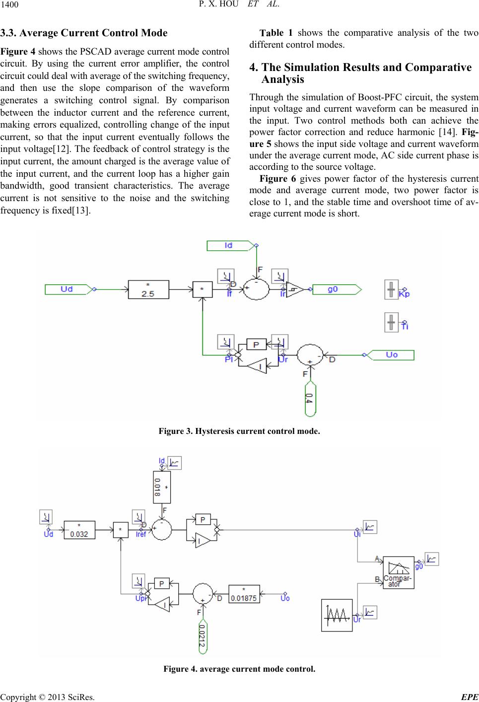 P. X. HOU ET AL. Copyright © 2013 SciRes. EPE 1400 3.3. Average Current Control Mode Table 1 shows the comparative analysis of the two different control modes. Figure 4 shows the PSCAD average current mode control circuit. By using the current error amplifier, the control circuit could deal with average of the switching frequency, and then use the slope comparison of the waveform generates a switching control signal. By comparison between the inductor current and the reference current, making errors equalized, controlling change of the input current, so that the input current eventually follows the input voltage[12]. The feedb ack of control strategy is the input current, the amount charged is the average value of the input current, and the current loop has a higher gain bandwidth, good transient characteristics. The average current is not sensitive to the noise and the switching frequency is fixed[13]. 4. The Simulation Results and Comparative Analysis Through the simulation of Boost-PFC circuit, the system input voltage and current waveform can be measured in the input. Two control methods both can achieve the power factor correction and reduce harmonic [14]. Fig- ure 5 shows the input side voltage and current waveform under th e avera ge cu rrent mo de, AC side curren t phas e is according to the source voltage. Figure 6 gives power factor of the hysteresis current mode and average current mode, two power factor is close to 1, and the stable time and overshoot time of av- erage current mode is short. Figure 3. Hysteresis current control mode. Figure 4. average current mode control. 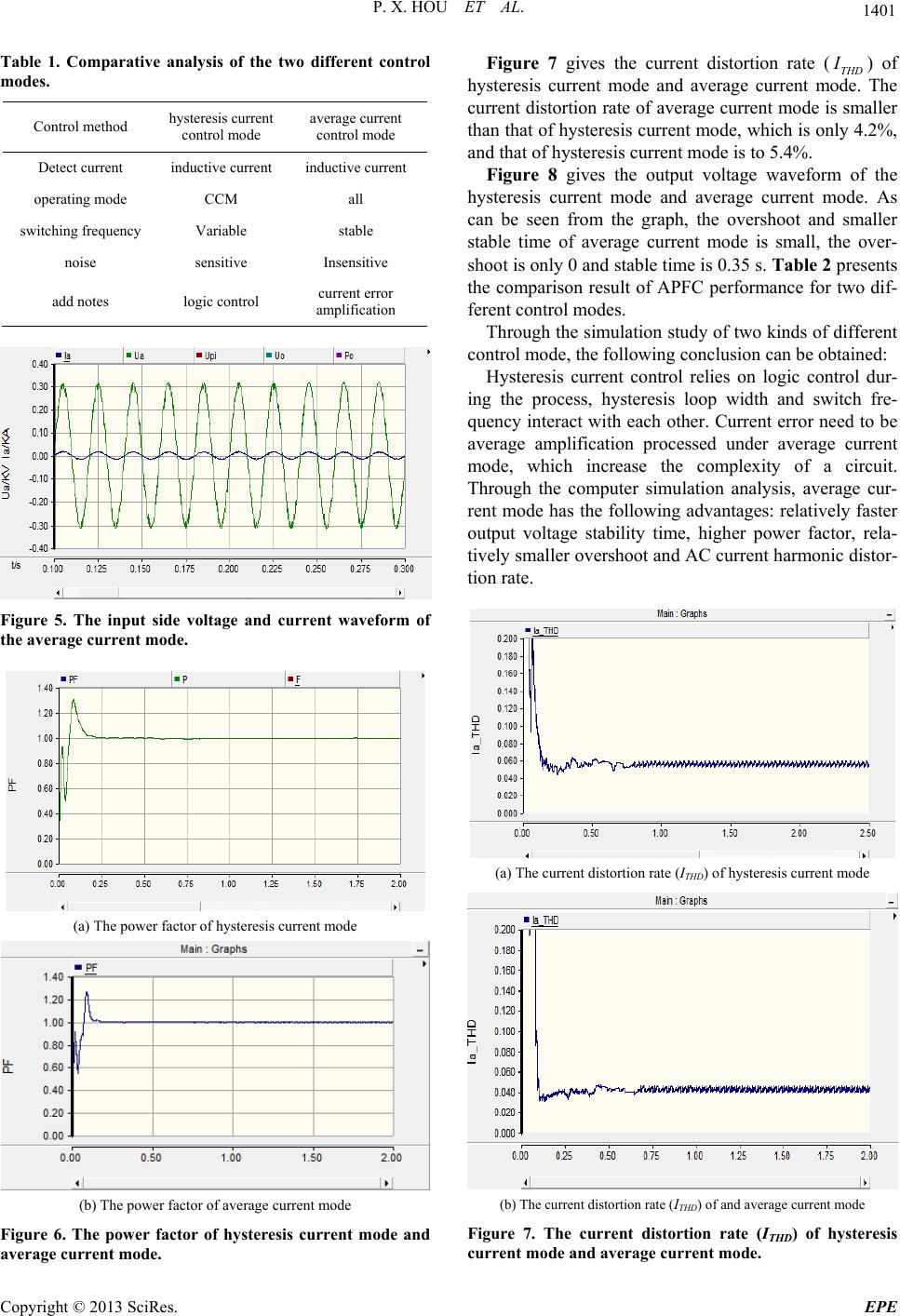 P. X. HOU ET AL. 1401 Table 1. Comparative analysis of the two different control modes. Control method hysteresis current control mode average current control mode Detect current inductive current inductive current operating mode CCM all switching frequency Variable stable noise sensitive Insensitive add notes logic control current error amplification Figure 5. The input side voltage and current waveform of the average current mode. (a) The power factor of hysteresis current mode (b) The power factor of average current mode Figure 6. The power factor of hysteresis current mode and average current mode. Figure 7 gives the current distortion rate (THD I ) of hysteresis current mode and average current mode. The current distortion rate of averag e current mode is smaller than that of hysteresis current mode, which is only 4.2%, and that of hysteresis current mode is to 5.4%. Figure 8 gives the output voltage waveform of the hysteresis current mode and average current mode. As can be seen from the graph, the overshoot and smaller stable time of average current mode is small, the over- shoot is only 0 and stable time is 0.35 s. Table 2 presents the comparison result of APFC performance for two dif- ferent control modes. Through the simulation study of two kinds of different control mode, the following conclusion can be obtained: Hysteresis current control relies on logic control dur- ing the process, hysteresis loop width and switch fre- quency interact with each other. Current error need to be average amplification processed under average current mode, which increase the complexity of a circuit. Through the computer simulation analysis, average cur- rent mode has the following advantages: relatively faster output voltage stability time, higher power factor, rela- tively smaller overshoot and AC current harmonic distor- tion rate. (a) The current distortion rate (ITHD) of hysteresis current mode (b) The current distortion rate (ITHD) of and average current mode Figure 7. The current distortion rate (ITHD) of hysteresis current mode and average current mode. Copyright © 2013 SciRes. EPE 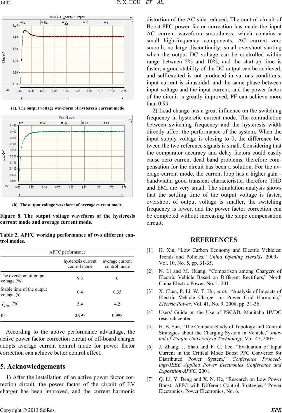 P. X. HOU ET AL. 1402 (a). The output voltage waveform of hysteresis current mode (b). The output voltage waveform of average current mode. Figure 8. The output voltage waveform of the hysteresis current mode and average current mode. Table 2. APFC working performance of two different con- trol modes. APFC performance hysteresis current control mode average current control mode The overshoot of output voltage (%) 9.3 0 Stable time of the outpu t voltage (s) 0.4 0.35 THD I(%) 5.4 4.2 PF 0.997 0.998 According to the above performance advantage, the active power factor correction circuit of off-board charger adopts average current control mode for power factor correction can achieve better control effect. 5. Acknowledgements 1) After the installation of an active power factor cor- rection circuit, the power factor of the circuit of EV charger has been improved, and the current harmonic distortion of the AC side reduced. The control circuit of Boost-PFC power factor correction has made the input AC current waveform smoothness, which contains a small high-frequency components; AC current zero smooth, no large discontinuity; small overshoot starting when the output DC voltage can be controlled within range between 5% and 10%, and the start-up time is faster; a good stability of the DC output can be achieve d, and self-excited is not produced in various conditions; input current is sinusoidal, and the same phase between input voltage and the input current, and the power factor of the circuit is greatly improved, PF can achieve more than 0.99. 2) Load change has a great influence on the switching frequency in hysteretic current mode. The contradiction between switching frequency and the hysteresis width directly affect the performance of the system. When the input supply voltage is closing to 0, the difference be- tween the two reference signals is small. Considering th at the comparator accuracy and delay factors could easily cause zero current dead band problems, therefore com- pensation for the circuit has been a solution. For the av- erage current mode, the current loop has a higher gain - bandwidth, good transient characteristic, therefore THD and EMI are very small. The simulation analysis shows that the settling time of the output voltage is faster, overshoot of output voltage is smaller, the switching frequency is lower, and the power factor correction can be completed without increasing the slope compensation circuit. REFERENCES [1] H. Xin, “Low Carbon Economy and Electric Vehicles: Trends and Policies,” China Opening Herald,2009, Vol. 10, No. 5, pp. 31-35. [2] N. Li and M. Huang, “Comparison among Chargers of Electric Vehicle Based on Different Rectifiers,” North China Electric Power. No. 1, 2011. [3] X. Chen, P. Li, W. T. Hu, et al., “Analysis of Impacts of Electric Vehicle Charger on Power Grid Harmonic,” Electric Power, Vol. 41, No. 9, 2008, pp. 31-36. [4] Users' Guide on the Use of PSCAD, Manitabo HVDC research center. [5] H. B. Sun, “The Compare-Study of Topology and Control Strategies about the Charging System in Vehicle,” Jour- nal of Tianjin University of Technology, Vol. 47, 2007. [6] J. Zhang, J. Shao and F. C. Lee, “Evaluation of Input Current in the Critical Mode Boost PFC Converter for Distributed Power System,” Conference Proceed- ings-IEEE Applied Power Electronics Conference and Exposition-APFC, 2001. [7] Q. Li, Y. Deng and X. N. He, “Research on Low Power Boost. APFC with Different Control Strategies,” Power Electronics. Power Electronics, No. 6. Copyright © 2013 SciRes. EPE  P. X. HOU ET AL. Copyright © 2013 SciRes. EPE 1403 [8] O. Garcia,J. A. Cobos, R. Prieto, et al., “Single Phase Power Factor Correction: A Survey,” IEEE Transactions, Vol. 18, No. 3, 2003, pp. 749-755. [9] H. Stork, “Changing the rules in Power Electronics,” IEEE Applied Power Electronics Conference and Exposi- tion, APEC’ 2005, Austin, Texas, Vol. 1, 2005, pp. 26-31. [10] Y. H. Tian, X. H. Wang and J. H. Lu, “The Design and Simulation of Single Phase Boost Power Factor Corrector Circuit,” Journal of Jiamusi University, Nov2008. Vol.26, No.6. [11] G. W. Moon, “Predictive Current Control of Distribution Static Compensator for Reactive Power Compensation,” IEE Proceedings of Gener Transm. Distrib. 1999, pp. 515-520. doi:10.1049/ip-gtd:19996598 [12] L. Qi, Z. Q. Xi, Z. Q. Xin and W. C. Huang, “Research on Single Phase APFC with Method of Hysteresis Con- trol,” Editorial Department of Hubei University of Tech- nology, Vol. 25, No. 1, 2010, pp. 52-54. [13] Y. F. Zhou,J. C. Huang, S. B. Wang, et al., “Principle of Designing Slope Compensation in PFC Boost con- verter,” Sci China Ser I, Vol. 52, No. 11, 2009, pp. 2226-2233. doi:10.1007/s11432-009-0178-6 [14] H. Wang, X. J. Yang and X. Cai, “Study and Implemen- tation of Digital APFC on Variable PI Regulator,” Power Electronics, Vol. 45, No. 1, 2011. |