

Paper Menu >>
Journal Menu >>
 Energy and Power Engineering, 2013, 5, 1215-1220 doi:10.4236/epe.2013.54B230 Published Online July 2013 (http://www.scirp.org/journal/epe) The Development of Network based Composite Power quality Regulation Device Weiqiang Fan, Ying Lei, Jing Zhu, Luo Li, Shuai Niu New energy technology research department, Xi’an High Voltage Apparatus Research Institute Co. Ltd, Xi’an, China Email: [email protected] Received March, 2013 ABSTRACT First, the paper analyzes the advantages and disadvantages of all kinds of reactive power compensation technology, and then proposes a principle and integrated control strategy of the composite operation of TSC and SVG, also the paper designs and develops the main co ntroller of Network based composite power qu ality regulatio n device, based on RTDS, the real-time digital simulation model of The Device is established, and finally the prototype of the device is developed with the function of filter and split-phase compensation. The main controller determines the cooperative operation of both TSC and SVG, and the switching strategy of TSC. The simulation result in RTDS can verify the precision of the measure system and the validity of the control logic, the prototype has finished the type test according to the national standard. Keywords: Network Based; Composite Power Quality Regulation Device; Reactive Power Compensation Technology; RTDS 1. Introduction With the rapid development of national economy,the amount and variety of power consumption equipment connected to the distribution network are also increasing, which causes the growing decline in the power quality characterized by the large amount of reactive power and serious harmonic pollution, so the effective method in improving power quality is to adopt reactive power compensation technology and harmonic suppression technology [1,2]. After decades of development, a variety of reactive power compensation devices have emerged. The cost and technical content of MSC is low but its poor dynamic compensation effect may bring many negative influence behind; The advantage of TSC is low cost, the sin- gle-tuned filter, large compensation capacity, split-phase compensation etc, but it can only achieve the step regula- tion of reactive power but cannot suppress voltage flicker; The TCR+FC type has the dynamic and smooth regulat- ing characteristics, but it can produce large harmonics and the grid voltage have a impact on its compensation capacity, which usually cause high fault rate. The SVG can realize continuous reactive compensation and sup- press voltage flicker, but its disadvantages lie in high cost and high-power switch device’s impact on its com- pensation capacity [3-5 ]. Xi’an High Voltage Apparatus Research Institute Co. Ltd has developed a novel via compensator——Network based composite power quality regulation device, which consists of several TSC banks and a SVG, by making fu ll use of TSC’s long-term stable reactive power compensa- tion and power harmonic suppression and SVG’s instant fast reactive pow er compensation, the r apidly continuous large-capacity reactive compensation can be realized, so this device not only compensates the reactive power and harmonic but also has a high performance price ratio compared to counterpart device. 2. Device Function Requirement and Construction Principle Design 2.1. Function Requirement In order to improve power factor more effectively and stabilize grid voltage, and then improve the grid power quality, The Device should have following basic func- tions. 1) Dynamically continuous reactive power compensa- tion, the power factor is always close to 1 when the de- vice’s capacity meets the demands. 2) The function of specific harmonic filter, the grid-side harmonic current injected by user can meet national harmonic standard when the device’s capacity meets the demands. 3) The ability to compensate unbalanced three-phase reactive power (split-phase compensation). Copyright © 2013 SciRes. EPE 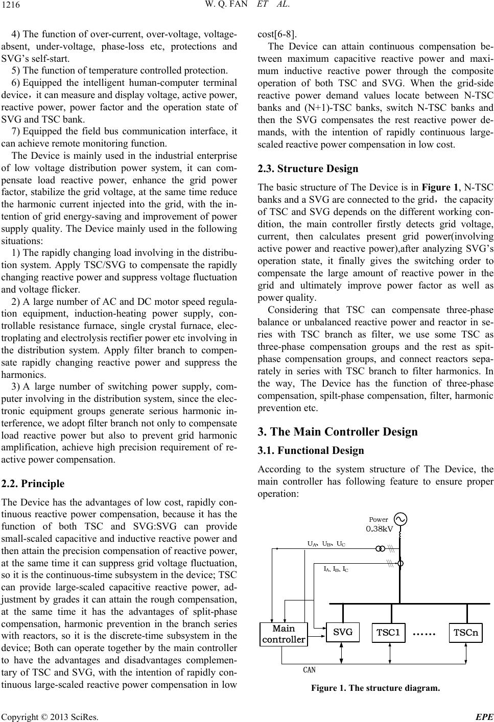 W. Q. FAN ET AL. 1216 4) The function of over-current, over-voltage, voltage- absent, under-voltage, phase-loss etc, protections and SVG’s self-start. 5) The function of temperature controlled protection. 6) Equipped the intelligent human-computer terminal device,it can measure and display voltage, active power, reactive power, power factor and the operation state of SVG and TSC bank. 7) Equipped the field bus communication interface, it can achieve remote monitoring function. The Device is mainly used in the industrial enterprise of low voltage distribution power system, it can com- pensate load reactive power, enhance the grid power factor, stabilize the grid voltage, at the same time reduce the harmonic current injected into the grid, with the in- tention of grid energy-saving and improvement of power supply quality. The Device mainly used in the following situations: 1) The rapidly changing load involving in the distribu- tion system. Apply TSC/SVG to compensate the rapidly changing reactive power and suppress voltage fluctuation and voltage flicker. 2) A large number of AC and DC mo tor speed reg ula- tion equipment, induction-heating power supply, con- trollable resistance furnace, single crystal furnace, elec- troplating and electrolysis rectifier power etc involving in the distribution system. Apply filter branch to compen- sate rapidly changing reactive power and suppress the harmonics. 3) A large number of switching power supply, com- puter involving in the distribution system, since the elec- tronic equipment groups generate serious harmonic in- terference, we adopt filter branch not only to compensate load reactive power but also to prevent grid harmonic amplification, achieve high precision requirement of re- active power compensation. 2.2. Principle The Device has the advantages of low cost, rapidly con- tinuous reactive power compensation, because it has the function of both TSC and SVG:SVG can provide small-scaled capacitive and inductive reactive power and then attain the precision compensation of reactive power, at the same time it can suppress grid voltage fluctuation, so it is the continuous-time subsystem in the device; TSC can provide large-scaled capacitive reactive power, ad- justment by grades it can attain the rough compensation, at the same time it has the advantages of split-phase compensation, harmonic prevention in the branch series with reactors, so it is the discrete-time subsystem in the device; Both can operate together by the main controller to have the advantages and disadvantages complemen- tary of TSC and SVG, with the intention of rapidly con- tinuous large-scaled reactive power compensation in low cost[6-8]. The Device can attain continuous compensation be- tween maximum capacitive reactive power and maxi- mum inductive reactive power through the composite operation of both TSC and SVG. When the grid-side reactive power demand values locate between N-TSC banks and (N+1)-TSC banks, switch N-TSC banks and then the SVG compensates the rest reactive power de- mands, with the intention of rapidly continuous large- scaled reactive power compensation in low cost. 2.3. Structure Design The basic structure of The Device is in Figure 1, N-TSC banks and a SVG are connected to the grid,the capacity of TSC and SVG depends on the different working con- dition, the main controller firstly detects grid voltage, current, then calculates present grid power(involving active power and reactive power),after analyzing SVG’s operation state, it finally gives the switching order to compensate the large amount of reactive power in the grid and ultimately improve power factor as well as power quality. Considering that TSC can compensate three-phase balance or unbalanced reactive power and reactor in se- ries with TSC branch as filter, we use some TSC as three-phase compensation groups and the rest as spit- phase compensation groups, and connect reactors sepa- rately in series with TSC branch to filter harmonics. In the way, The Device has the function of three-phase compensation, spilt-phase compensation, filter, harmonic prevention etc. 3. The Main Controller Design 3.1. Functional Design According to the system structure of The Device, the main controller has following feature to ensure proper operation: Figure 1. The structure diagram. Copyright © 2013 SciRes. EPE 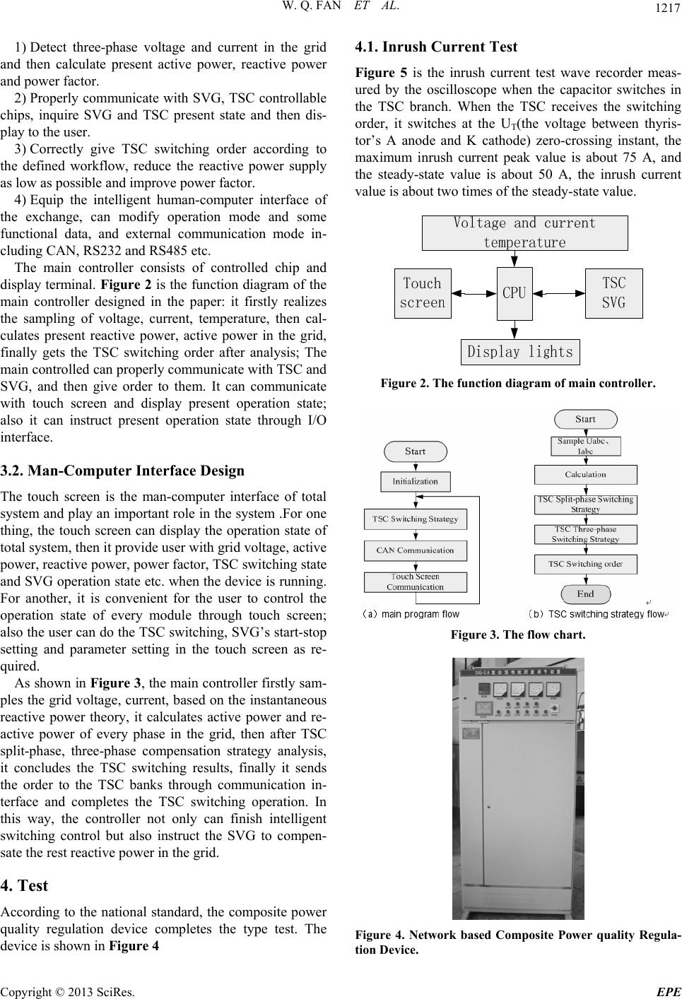 W. Q. FAN ET AL. 1217 1) Detect three-phase voltage and current in the grid and then calculate present active power, reactive power and power factor. 2) Properly communicate with SVG, TSC controllable chips, inquire SVG and TSC present state and then dis- play to the user. 3) Correctly give TSC switching order according to the defined workflow, reduce the reactive power supply as low as possible and improve power factor. 4) Equip the intelligent human-computer interface of the exchange, can modify operation mode and some functional data, and external communication mode in- cluding CAN, RS232 and RS485 etc. The main controller consists of controlled chip and display terminal. Figure 2 is the function diagram of the main controller designed in the paper: it firstly realizes the sampling of voltage, current, temperature, then cal- culates present reactive power, active power in the grid, finally gets the TSC switching order after analysis; The main controlled can prop erly communicate with TSC and SVG, and then give order to them. It can communicate with touch screen and display present operation state; also it can instruct present operation state through I/O interface. 3.2. Man-Computer Interface Design The touch screen is the man-computer interface of total system and play an important role in the syste m .For one thing, the touch screen can display the operation state of total system, then it provide user with grid voltage, active power, reactive power, power factor, TSC switching state and SVG operation state etc. when the device is runn ing. For another, it is convenient for the user to control the operation state of every module through touch screen; also the user can do the TSC switching, SVG’s start-stop setting and parameter setting in the touch screen as re- quired. As shown in Figure 3, the main controller firstly sam- ples the grid voltage, current, based on the instantaneous reactive power theory, it calculates active power and re- active power of every phase in the grid, then after TSC split-phase, three-phase compensation strategy analysis, it concludes the TSC switching results, finally it sends the order to the TSC banks through communication in- terface and completes the TSC switching operation. In this way, the controller not only can finish intelligent switching control but also instruct the SVG to compen- sate the rest reactive power in the grid. 4. Test According to the national standard, the composite power quality regulation device completes the type test. The device is shown in Figure 4 4.1. Inrush Current Test Figure 5 is the inrush current test wave recorder meas- ured by the oscilloscope when the capacitor switches in the TSC branch. When the TSC receives the switching order, it switches at the UT(the voltage between thyris- tor’s A anode and K cathode) zero-crossing instant, the maximum inrush current peak value is about 75 A, and the steady-state value is about 50 A, the inrush current value is about two times of the steady-state value. Figure 2. The function diagram of main controller. Figure 3. The flow chart. Figure 4. Network based Composite Power quality Regula- tion Device. Copyright © 2013 SciRes. EPE 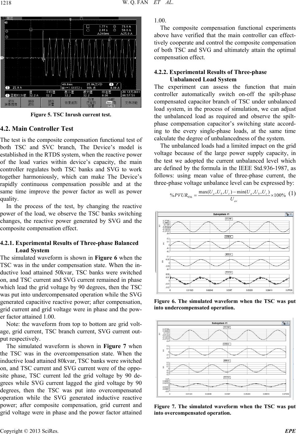 W. Q. FAN ET AL. 1218 Figure 5. TSC Inrush current test. 4.2. Main Controller Test The test is the composite compensation functional test of both TSC and SVC branch, The Device’s model is established in the RTDS system, when the reactive power of the load varies within device’s capacity, the main controller regulates both TSC banks and SVG to work together harmoniously, which can make The Device’s rapidly continuous compensation possible and at the same time improve the power factor as well as power quality. In the process of the test, by changing the reactive power of the load, we observe the TSC banks switching changes, the reactive power generated by SVG and the composite compensation effect. 4.2.1. Experimental Results of Three-phase Balanced Load System The simulated waveform is shown in Figure 6 when the TSC was in the under compensation state. When the in- ductive load attained 50kvar, TSC banks were switched on, and T SC current and SVG cu rrent remained in phase which lead the grid voltage by 90 degrees, then the TSC was put into undercompensated operation while th e SVG generated capacitive reactive power; after compensation, grid current and grid voltage were in phase and the pow- er factor attained 1.00. Note: the waveform from top to bottom are grid volt- age, grid current, TSC branch current, SVG current out- put respectively. The simulated waveform is shown in Figure 7 when the TSC was in the overcompensation state. When the inductive load attained 80k var, TSC banks were switched on, and TSC current and SVG current were of the oppo- site phase, TSC current led the grid voltage by 90 de- grees while SVG current lagged the gird voltage by 90 degrees, then the TSC was put into overcompensated operation while the SVG generated inductive reactive power; after composite compensation, grid current and grid voltage were in phase and the power factor attained 1.00. The composite compensation functional experiments above have verified that the main controller can effect- tively cooperate and control the composite compensation of both TSC and SVG and ultimately attain the optimal compensation effect. 4.2.2. Experimental Results of Three-phase Unbalanced Load System The experiment can assess the function that main controller automatically switch on-off the spilt-phase compensated capacitor branch of TSC under unbalanced load system, in the process of simulation, we can adjust the unbalanced load as required and observe the spilt- phase compensation capacitor’s switching state accord- ing to the every single-phase loads, at the same time calculate the degree of unbalancedness of the system. The unbalanced loads had a limited impact on the grid voltage because of the large power supply capacity, in the test we adopted the current unbalanced level which are defined by the formula in the IEEE Std.936-1987, as follows: using mean value of three-phase current, the three-phase voltage unbalance level can be expressed by: 936 max(,,)min(,,) % 100% abc abc av UUU UUU PVUR U (1) Figure 6. The simulated waveform when the TSC was put into undercompensated operation. Figure 7. The simulated waveform when the TSC was put into overcompensated operation. Copyright © 2013 SciRes. EPE 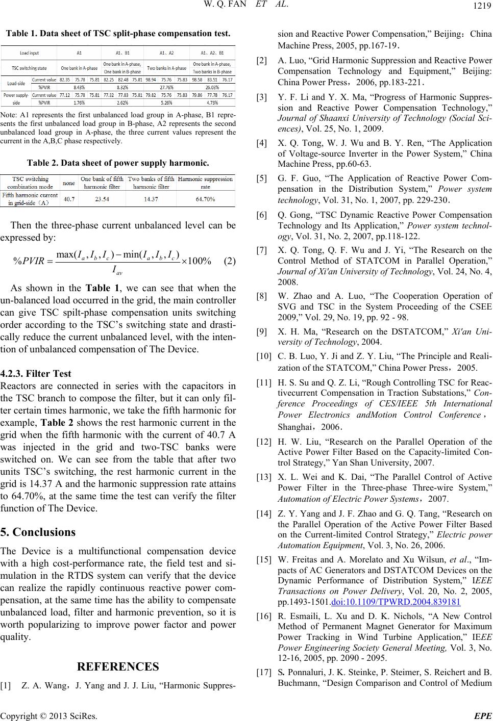 W. Q. FAN ET AL. 1219 Table 1. Data sheet of TSC split-phase compensation test. Note: A1 represents the first unbalanced load group in A-phase, B1 repre- sents the first unbalanced load group in B-phase, A2 represents the second unbalanced load group in A-phase, the three current values represent the current in the A,B,C phase respectively. Table 2. Data sheet of power supply harmonic. Then the three-phase current unbalanced level can be expressed b y : max( ,,) min( ,,) % abc abc av III III PVIR I 100% (2) As shown in the Table 1, we can see that when the un-balanced load occurred in the grid, the main controller can give TSC spilt-phase compensation units switching order according to the TSC’s switching state and drasti- cally reduce the current unbalanced level, with th e inten- tion of unbalanced compensation of The Device. 4.2.3. Fi lter Test Reactors are connected in series with the capacitors in the TSC branch to compose the filter, but it can only fil- ter certain times harmonic, we take the fifth harmonic for example, Table 2 shows the rest harmonic current in the grid when the fifth harmonic with the current of 40.7 A was injected in the grid and two-TSC banks were switched on. We can see from the table that after two units TSC’s switching, the rest harmonic current in the grid is 14.37 A and the harmonic suppression rate attains to 64.70%, at the same time the test can verify the filter functio n o f The Device. 5. Conclusions The Device is a multifunctional compensation device with a high cost-performance rate, the field test and si- mulation in the RTDS system can verify that the device can realize the rapidly continuous reactive power com- pensation, at the same time has the ability to co mpensate unbalanced load, filter and harmonic prevention, so it is worth popularizing to improve power factor and power quality. REFERENCES [1] Z. A. Wang,J. Yang and J. J. Liu, “Harmonic Suppres- sion and Reactive Power Compensation,” Beijing:China Machine Press, 2005, pp.167-19. [2] A. Luo, “Grid Harmonic Suppression and Reactive Power Compensation Technology and Equipment,” Beijing: China Power Press,2006, pp.183-221. [3] Y. F. Li and Y. X. Ma, “Progress of Harmonic Suppres- sion and Reactive Power Compensation Technology,” Journal of Shaanxi University of Technology (Social Sci- ences), Vol. 25, No. 1, 2009. [4] X. Q. Tong, W. J. Wu and B. Y. Ren, “The Application of Voltage-source Inverter in the Power System,” China Machine Press, pp.60-63. [5] G. F. Guo, “The Application of Reactive Power Com- pensation in the Distribution System,” Power system technology, Vol. 31, No. 1, 2007, pp. 229-230. [6] Q. Gong, “TSC Dynamic Reactive Power Compensation Technology and Its Application,” Power system technol- ogy, Vol. 31, No. 2, 2007, pp.118-122. [7] X. Q. Tong, Q. F. Wu and J. Yi, “The Research on the Control Method of STATCOM in Parallel Operation,” Journal of Xi'an University of Technology, Vol. 24, No. 4, 2008. [8] W. Zhao and A. Luo, “The Cooperation Operation of SVG and TSC in the System Proceeding of the CSEE 2009,” Vol. 29, No. 19, pp. 92 - 98. [9] X. H. Ma, “Research on the DSTATCOM,” Xi'an Uni- versity of Technology, 2004. [10] C. B. Luo, Y. Ji and Z. Y. Liu, “The Principle and Reali- zation of the STATCOM,” China Power Press,2005. [11] H. S. Su and Q. Z. Li, “Rough Controlling TSC for Reac- tivecurrent Compensation in Traction Substations,” Con- ference Proceedings of CES/IEEE 5th International Power Electronics andMotion Control Conference, Shanghai,2006. [12] H. W. Liu, “Research on the Parallel Operation of the Active Power Filter Based on the Capacity-limited Con- trol Strategy,” Yan Shan University, 2007. [13] X. L. Wei and K. Dai, “The Parallel Control of Active Power Filter in the Three-phase Three-wire System,” Automation of Electric Power Syste ms,2007. [14] Z. Y. Yang and J. F. Zhao and G. Q. Tang, “Research on the Parallel Operation of the Active Power Filter Based on the Current-limited Control Strategy,” Electric power Automation Equipment, Vol. 3, No. 26, 2006. [15] W. Freitas and A. Morelato and Xu Wilsun, et al., “Im- pacts of AC Generators and DSTATCOM Devices on the Dynamic Performance of Distribution System,” IEEE Transactions on Power Delivery, Vol. 20, No. 2, 2005, pp.1493-1501.doi:10.1109/TPWRD.2004.839181 [16] R. Esmaili, L. Xu and D. K. Nichols, “A New Control Method of Permanent Magnet Generator for Maximum Power Tracking in Wind Turbine Application,” IEEE Power Engineering Society General Meeting, Vol. 3, No. 12-16, 2005, pp. 2090 - 2095. [17] S. Ponnaluri, J. K. Steinke, P. Steimer, S. Reichert and B. Buchmann, “Design Comparison and Control of Medium Copyright © 2013 SciRes. EPE  W. Q. FAN ET AL. Copyright © 2013 SciRes. EPE 1220 Voltage STATCOM with Novel Twin Converter Topol- ogy,” 35th Annul IEEE Power Electronics Specialists Conference, 2004. [18] M. S. ElMoursi, Prof. Dr. A. M.Sharaf, “Voltage Stabili- zation And Reactive Compensation Using A Novel FACTS-STATCOM Scheme,” IEEE CCECE/CCGEI, Saskatoon, May 2005. |