

Paper Menu >>
Journal Menu >>
 Journal of Biosciences and Medicines, 2013, 1, 1-5 JBM http://dx.doi.org/10.4236/jbm.2013.12001 Published Online October 2013 (http://www.scirp.org/journal/jbm/) OPEN ACCESS A spatiotemporal signal processing technique for wafer-scale IC thermomechanical stress monitoring by an infrared camera Michel Saydé, Ahmed Lakhssassi, Emmanuel Kengne, Roman Palenichka Department of Computer Sciences and engineering, University of Quebec at Outaouais, Gatineau, Canada Email: [email protected], ahmed[email protected], [email protected], [email protected] Received July 2013 ABSTRACT In this paper, we describe a new silicon-die thermal monitoring approach using spatiotemporal signal processing technique for Wafer-Scale IC thermome- chanical stress monitoring. It is proposed in the con- text of a wafer-scale-based (WaferICTM) rapid proto- typing platform for electronic systems. This technique will be embedded into the structure of the WaferIC, and will be used as a preventive measure to protect the wafer from possible damages that can be caused by excessive thermomechanical stress. The paper also presents spatial and spatiotemporal algorithms and the experimental results from an IR images collection campaign conducted using an IR camera. Keywords: Thermal Monitoring; Ring Oscillator (RO); Spatial; Spatiotemporal; Thermo-Mechanical Stress; Temperature Sensor; Thermal Analysis; WaferIC; Wafer-Scale System 1. INTRODUCTION An innovative reconfigurable Wafer-Scale Integrated Circuit (WaferIC) for rapid electronic systems prototyp- ing has been introduced [1-3]. Electronic components can be placed anywhere at the smart active surface of the WaferIC. Then those components can be detected, pow- ered and interconnected through a complex but regular reconfigurable network laid over the surface of the WaferIC. As power consumption depends on user chips location and power pins distribution, it is not even ly dis- tributed throughout the surface of the silicon wafer. In many cases, it is unpredictable and variable as power consumption of programmable or dynamic components (e.g. microcontroller s) depends on their activities. There- fore, managing thermomechanical stress is a real chal- lenge and it may need to be monitored at all time in high performance applications. Thermal monitoring is essential in high performance integrated structures implemented as multilayer struc- tures composed of different materials. An increase of the internal temperature of some circuits can lead to signifi- cant thermal and thermo-mechanical problems. Under- standing thermal phenomena occurring on a micro-scale level is essential for SoC and MEMS -based applications. Thus, measurement techniques are needed to validate models predicting thermal behavior of integrated struc- tures. In particular, measurement techniques are needed to obtain surface temperature distributions of large inte- grated structures. Due to technology scaling, power density of high per- formance integrated structures has increased drastically. For example, the power density of high performance microprocessors has already reached 50 W/cm2 at 100 nm technology and was forecasted to reach 100 W/cm2 at 20 nm technology. Meanwhile, to mitigate the overall power consumption, many low power techniques have been proposed [4-10]. These techniques, though helpful to reduce the overall power consumption, may cause sig- nificant on-chip thermal gradients and local hot spots due to different clock/power gating activities and varying voltage scaling. It has been reported in [11] that temper- ature variations of 30˚C can occur in a high performance microprocessor design. The magnitude of thermal gra- dients and associated thermo-mechanical stress is ex- pected to increase further as VLSI designs move into nanometer processes and multi-GHz frequencies. The WaferIC is a LAIC (Large Area Integrated Cir- cuit). As a LAIC the increase of the power consumption and uIC disposition on the surface of the WaferIC will cause decrease in the wafer performance and the latency. In addition, 50% of the failure in the electronic device is due to the increase of the internal temperature of the chip [12]. However, the WaferIC must be able to support a large temperature differential at its surface [13]. There- fore, in this paper we propose a spatiotemporal signal processing technique for Wafer-Scale IC thermomechan- ical stress monitoring by an infrared camera. The tech- 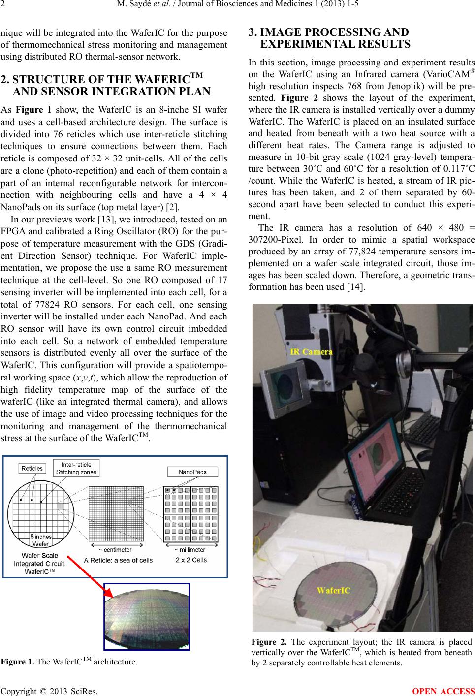 M. Saydé et al. / Journal of Biosciences and Medicines 1 (2013) 1-5 Copyright © 2013 SciRes. OPEN ACCESS 2 nique will be integrated into the WaferI C for the purpos e of thermomechanical stress monitoring and management using distributed RO thermal-sensor networ k. 2. STRUCTURE OF THE WAFERICTM AND SENSOR INTEGRATION PLAN As Figure 1 show, the WaferIC is an 8-inche SI wafer and uses a cell-based architecture design. The surface is divided into 76 reticles which use inter-reticle stitching techniques to ensure connections between them. Each reticle is composed of 32 × 32 unit-cells. All of the cells are a clone (photo-repetition) and each of them contain a part of an internal reconfigurable network for intercon- nection with neighbouring cells and have a 4 × 4 NanoPads on its surface (top metal layer) [2]. In our previews work [13], we introduce d, tes ted on an FPGA and calibrated a Ring Oscillator (RO) for the pu r- pose of temperature measurement with the GDS (Gradi- ent Direction Sensor) technique. For WaferIC imple- mentation, we propose the use a same RO measurement technique at the cell-level. So one RO composed of 17 sensing inverter will be implemented into each cell, for a total of 77824 RO sensors. For each cell, one sensing inverter will be installed under each NanoPad. And each RO sensor will have its own control circuit imbedded into each cell. So a network of embedded temperature sensors is distributed evenly all over the surface of the WaferIC. This configuration will provide a spatiotempo- ral working space (x,y,t), which allow the reproduction of high fidelity temperature map of the surface of the waferIC (like an integrated thermal camera), and allows the use of image and video processing techniques for the monitoring and management of the thermomechanical stress at the surface of the WaferICTM. Figure 1. The WaferICTM architecture. 3. IMAGE PROCESSING AND EXPERIMENTAL RESULTS In this section, image processing and experiment results on the WaferIC using an Infrared camera (VarioCAM® high resolution inspects 768 from Jenoptik) will be pre- sented. Figure 2 show s the layout of the experiment, where the IR camera is installed v ertically over a dummy WaferIC. The WaferIC is placed on an insulated surface and heated from beneath with a two heat source with a different heat rates. The Camera range is adjusted to measure in 10-bit gray scale (1024 gray-level) tempera- ture between 30˚C and 60˚C for a resolution of 0.117˚C /count. While the WaferIC is heated, a stream of IR pic- tures has been taken, and 2 of them separated by 60- second apart have been selected to conduct this experi- ment. The IR camera has a resolution of 640 × 480 = 307200-Pixel. In order to mimic a spatial workspace produced by an array of 77,824 temperature sensors im- plemented on a wafer scale integrated circuit, those im- ages has been scaled down. Therefore, a geometric trans- formation has been used [14]. Figure 2. The experiment layout; the IR camera is placed vertically over the WaferICTM, which is heated from beneath by 2 separately controllable heat elements. 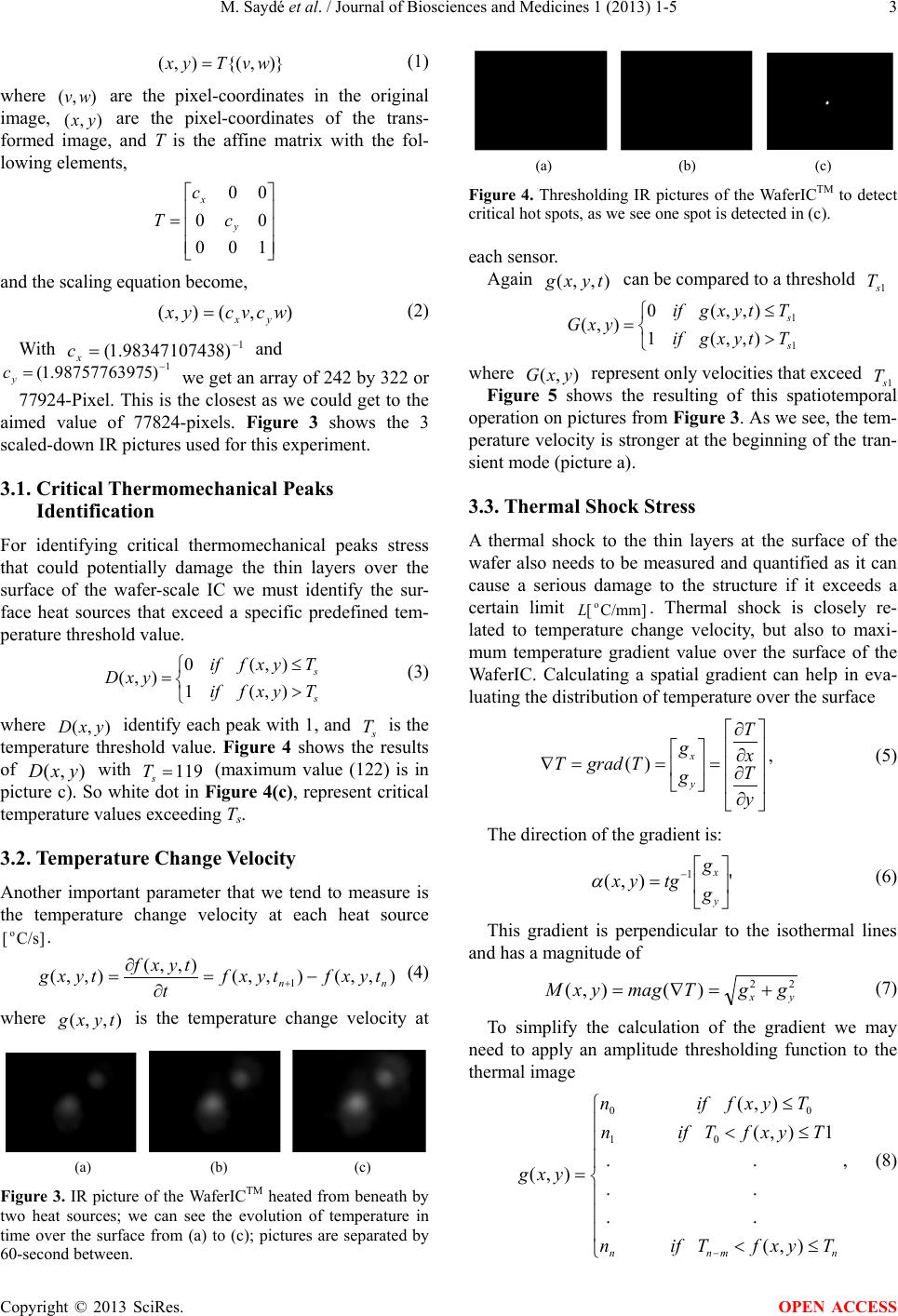 M. Saydé et al. / Journal of Biosciences and Medicines 1 (2013) 1-5 Copyright © 2013 SciRes. OPEN ACCESS 3 )},{(),( wvTyx = (1) where ),( wv are the pixel-coordinates in the original image, ),( yx are the pixel-coordinates of the trans- formed image, and T is the affine matrix with the fol- lowing elements, = 100 00 00 y x c c T and the scaling equation become, ),(),( wcvcyx yx = (2) With 1 )89834710743.1( − = x c and 1 )59875776397.1( − = y c we get an array of 242 by 322 or 77924-Pixel. This is the closest as we could get to the aimed value of 77824-pixels. Figure 3 shows the 3 scaled-down IR pic tures used for this ex pe riment . 3.1. Critical Thermomechanical Peaks Identification For identifying critical thermomechanical peaks stress that could potentially damage the thin layers over the surface of the wafer-scale IC we must identify the sur- face heat sources that exceed a specific predefined tem- perature threshol d va lue. > ≤ = s s Tyxfif Tyxfif yxD ),(1 ),(0 ),( (3) where ),( yxD identify each peak with 1, and s T is the temperature threshold value. Figure 4 shows the results of ),( yxD with 119= s T (maximum value (122) is in picture c). So white dot in Figure 4(c), represent critical temperature values exceeding Ts. 3.2. Temperature Change Velo city Another important parameter that we tend to measure is the temperature change velocity at each heat source o [ C/s] . ),,(),,( ),,( ),,( 1nn tyxftyxf t tyxf tyxg −= ∂ ∂ = + (4) where ),,( tyxg is the temperature change velocity at (a) (b) (c) Figure 3. IR picture of the WaferICTM heated from beneath by two heat sources; we can see the evolution of temperature in time over the surface from (a) to (c); pictures are separated by 60-second between. (a) (b) (c) Figure 4. Thresholding IR pictures of the WaferICTM to detect critical hot spots, as we see one spot is detected in (c). each sensor. Again ),,( tyxg can be compared to a threshold 1s T > ≤ = 1 1 ),,(1 ),,(0 ),( s s Ttyxgif Ttyxgif yxG where ),( yxG represent only velocities that exceed 1s T Figure 5 shows the resulting of this spatiotemporal operation on pictures from Figure 3. As we see, the tem- perature velocity is stronger at the beginning of the tran- sient mode (picture a). 3.3. Thermal Shock Stress A thermal shock to the thin layers at the surface of the wafer also needs to be measured and quantified as it can cause a serious damage to the structure if it exceeds a certain limit o [ C/mm]L . Thermal shock is closely re- lated to temperature change velocity, but also to maxi- mum temperature gradient value over the surface of the WaferIC. Calculating a spatial gradient can help in eva- luating the distribution of t emper ature over the surface ∂ ∂ ∂ ∂ = ==∇ y T x T g g TgradT y x )( , (5) The direction of the gradient is: '),( 1 = − y x g g tgyx α (6) This gradient is perpendicular to the isothermal lines and has a magnitude of 22 )(),( yx ggTmagyxM+=∇= (7 ) To simplify the calculation of the gradient we may need to apply an amplitude thresholding function to the thermal image nmnn TyxfTif TyxfTif Tyxfif n n n yxg ≤< ≤< ≤ = − ),( . . . 1),( ),( . . . ),( 0 0 1 0 , (8) 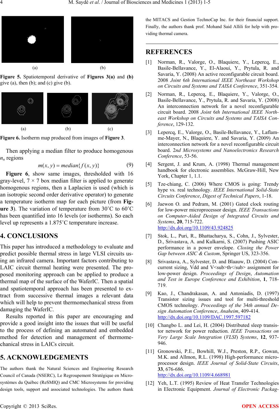 M. Saydé et al. / Journal of Biosciences and Medicines 1 (2013) 1-5 Copyright © 2013 SciRes. OPEN ACCESS 4 (a) (b) Figure 5. Spatiotemporal derivative of Figure s 3(a) and (b) give (a), then (b); and (c) give (b). (a) (b) (c) Figure 6. Isotherm map produced from images of Figure 3. Then applying a median filter to produce homogenous nn regions )},({),( yxfmedianyxm = (9) Figure 6, show same images, thresholded with 16 gray-level, 7 × 7 bo x median filter is applied to generate homogenous regions, then a Laplacien is used (which is an isotropic second order derivative operator) to generate a temperature isotherm map for each picture (from Fig- ure 3). The variation of temperature from 30˚C to 60˚C has been quantified into 16 levels (or isotherms). So each level up represents a 1.875˚C temperature increase. 4. CONCLUSIONS This paper has introduced a methodology to evaluate and predict possible thermal stress in large VLSI circuits us- ing an infrared camera. Important factors contributing to LAIC circuit thermal heating were presented. The pro- posed monitoring approach can be applied to produce a thermal map of the surface of the WaferIC. Then a spatial and spatiotemporal approach has been presented to ex- tract from successive thermal images a relevant data which will help to prevent thermomechanical stress from damagi ng the WaferIC . Results reported in this paper are encouraging and provide a good insight into the issues that will be useful to the process of defining an automated and embedded method for detection and management of thermome- chanical stress in LAICs circuit. 5. ACKNOWL EDG EMENTS The authors thank the Natural Sciences and Engineering Research Council of Canad a (NSERC), Le Regroupement Stratégiq ue en Micro- systèmes du Québec (ReSMIQ) and CMC Microsystems for prov iding design tools, support and associated technologies. The authors thank the MITACS and Gestion TechnoCap Inc. for their financial support. Finally, the authors thank prof. Mohand Said Allili for help with pro- viding thermal camera. REFERENCES [1] Norman, R., Valorge, O., Blaquiere, Y., Lepercq, E., Basile-Bellavance, Y., El-Alaoui, Y., Prytula, R. and Savaria, Y. (2008) An active reconfigurable circuit board. 2008 Joint 6th International IEEE Northeast Workshop on Circuits and Systems and TAISA Conference, 351-354. [2] Norman, R., Lepercq, E., Blaquiere, Y., Valorge, O., Basile-Bellavance, Y., Prytula, R. and Savaria, Y. (2008) An interconnection network for a novel reconfigurable circuit board. 2008 Joint 6th International IEEE North- east Workshop on Circuits and Systems and TAISA Con- ference, 129-132. [3] Lepercq, E., Valorge, O., Basile-Bellavance, Y., Laflam- me-Mayer, N., Blaquiere, Y. and Savaria, Y. (2009) An interconnection network for a novel reconfigurable circuit board. 2nd Microsystems and Nanoelectronics Research Conference, 53-56. [4] Sergent, J. and Krum, A. (1998) Thermal management handbook for electronic assemblies. McGraw-Hill, New York, Chapter 1, 1.1. [5] Tze-chiang, C. (2006) Where CMOS is going: Trendy hype vs. real technology. IEEE International Solid-State Circuits Conference, Digest of Technical Papers, 1-18. [6] Jaewon O. and Pedram, M. (2001) Gated clock routing for low-power microprocessor design. IEEE Transactions on Computer-Aided Design of Integrated Circuits and Systems, 20, 715-722. http://dx.doi.org/10.1109/43.924825 [7] Stok, L., Puri, R., Bhattacharya, S., Cohn, J., Sylvester, D., Srivastava, A. and Kulkarni, S. (2007) Pushing ASIC performance in a power envelope. Closing the Power Gap between ASIC & Custom, Springer US, 323-356. [8] Srivastava, A., Sylvester, D. and Blaauw, D. (2004) Con- current sizing, Vdd and V<sub>th</sub> assignment for low-power design. Proceedings of Desi gn, Automation and Test in Europe Conference and Exhibition, 1, 718- 719. [9] Kao, J., Chandrakasan, A. and Antoniadis, D. (1997) Transistor sizing issues and tool for multi-threshold CMOS technology. Proceedings of the 34th annual De- sign Automation Conference, Anaheim, 409-414. http://dx.doi.org/10.1109/DAC.1997.597182 [10] Changbo L. and Lei, H. (2004) Distributed sleep transis- tor network for power reduction. IEEE Transactions on Very Large Scale Integration (VLSI) Systems, 12, 937- 946. [11] Gronowski, P. E., Bowhill, W.J., Preston, R.P., Gowan, M.K. and Allmon, R.L. (1998) High-performance micro- processor design. IEEE Journal of Solid-State Circuits, 33, 676-686. http://dx.doi.org/10.1109/4.668981 [12] Yeh, L.T. (1995) Review of Heat Transfer Technologies in Electronic Equipment. Journal of Electronic Packag-  M. Saydé et al. / Journal of Biosciences and Medicines 1 (2013) 1-5 Copyright © 2013 SciRes. OPEN ACCESS 5 ing, 117, 333-339. http://dx.doi.org/10.1115/1.2792113 [13] Sayde, M., Berriah, O., Lakhssassi , A., Bougataya, M., Kengne, E. and Talbi, L. (2001) Silicon-die thermal mo- nitoring using embedded sensor cells unit. 2011 IEEE 9th International on New Circuits and Systems Conference (NEWCAS), 153-156. [14] Rafael P.H.D., Gonzalez C. and Woods, R.E. (2008) Digital image processing. 3rd Edition, Prentice Hall. |