

Paper Menu >>
Journal Menu >>
 Communications and Network, 2013, 5, 140-143 http://dx.doi.org/10.4236/cn.2013.53B2027 Published Online September 2013 (http://www.scirp.org/journal/cn) Three-Points Modulator Based on DPLL for Wideband Polar Modulation Julien Kieffer1, Sébastien Rieubon1, Marc Houdebine2, Sébastien Dedieu2, Emil Novakov3 1ST-Ericsson, Grenoble, France 2STMicroelectronics, Crolles, France 3IMEP-LAHC, University of Grenoble-Alpes, Grenoble, France Email: [email protected] Received May, 2013 ABSTRACT We present a nonlinear event-driven model of a Digital PLL used in the context of a polar modulation. This modeling has shown that the estimation method of the TDC gain has a big impact on the EVM for wideband modulation and a solution has been proposed which consists to add the modulation on the gain after calibration of the gain offset. This transforms the classical two-points modulator into a three-points modulator. This implementation has been validated for WCDMA standard. Keywords: DPLL; Polar Modulation; WCDMA; TDC 1. Introduction The number of wireless standards has expanded during the last decade, allowing the use of new applications such as internet for mobile or video calls for example. These new functions are very demanding in terms of de- bit rate. New communications standards have been de- veloped to follow this evolution such as WCDMA and LTE for mobile phone. Their requirements in terms of noises, spurious, consumption, etc. are more and more stringent and their bandwidths more and more wider. In this context, the polar transmitter as shown in Figure 1 seems to be an attractive architecture to reach these tough specifications. The typical IQ signal, produced by the modulator, is converted by a Coordinate Rotation Digital Computer (CORDIC) into a polar signal. Lots of studies of the am- plitude modulation by the Power Amplifier (PA) can be found in the literature[1,2], but the phase modulation by the PLL, which could be either analog or digital, seems to be less studied, especially for wideband modulations. This will be the core of this work. In order to study the phase path, the modeling of the PLL has to be even more and more accurate. Many fre- ency-domain models have been developed in the past years from the classic Laplace model which can be used to study transfer functions and PLL noises to more com- plex sampled models [3-5] which are now very useful for the study of polar modulation. The model of Digital PLL proposed in this paper allows even more precision in the modeling of the different blocks of the PLL by including noises and nonlinearities and still allows fast simulation because it is event driven. As already said, the main application for which our model has been developed is to observe the impact of a modulation passing directly through the PLL in the case of a polar modulation. e-point modulator can be used for narrowband modu- lations, where the bandwidth is lower than the PLL cut-off frequency. The modulation is transmitted by add- ing the modulation data to the PLL frequency command word. Meanwhile, modulation bandwidth can be slightly enlarged by using a pre-distortion filter which compen- sates the PLL low path filtering [8]. However, PLL fil- tering and pre-distortion transfer function fitting mis- matches limit the modulation bandwidth extension. Sev- eral methods for reducing the modulation bandwidth have also been proposed. Figure 1. Polar transmitter. C opyright © 2013 SciRes. CN 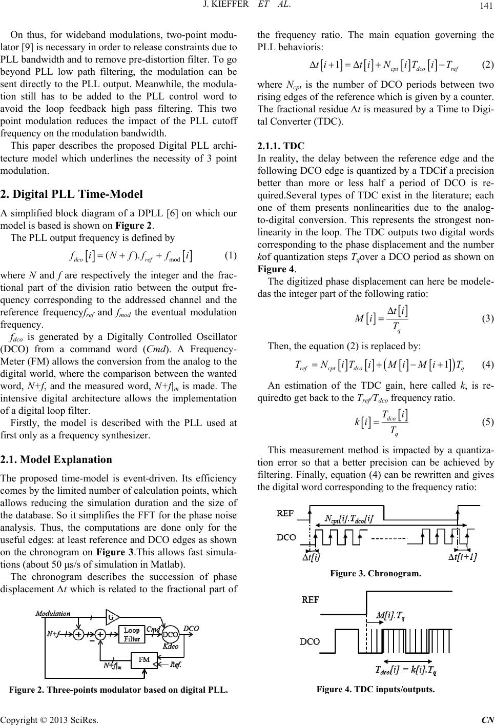 J. KIEFFER ET AL. 141 On thus, for wideband modulations, two-point modu- lator [9] is necessary in order to release constraints due to PLL bandwidth and to remove pre-distortion filter. To go beyond PLL low path filtering, the modulation can be sent directly to the PLL output. Meanwhile, the modula- tion still has to be added to the PLL control word to avoid the loop feedback high pass filtering. This two point modulation reduces the impact of the PLL cutoff frequency on the modulation bandwidth. This paper describes the proposed Digital PLL archi- tecture model which underlines the necessity of 3 point modulation. 2. Digital PLL Time-Model A simplified block diagram of a DPLL [6] on which our model is based is shown on Figure 2. The PLL output frequency is defined by mod (). dco ref f iNff fi (1) where N and f are respectively the integer and the frac- tional part of the division ratio between the output fre- quency corresponding to the addressed channel and the reference frequencyfref and fmod the eventual modulation frequency. fdco is generated by a Digitally Controlled Oscillator (DCO) from a command word (Cmd). A Frequency- Meter (FM) allows the conversion from the analog to the digital world, where the comparison between the wanted word, N+f, and the measured word, N+f|m is made. The intensive digital architecture allows the implementation of a digital loop filter. Firstly, the model is described with the PLL used at first only as a frequency synthesizer. 2.1. Model Explanation The proposed time-model is event-driven. Its efficiency comes by the limited number of calculation points, which allows reducing the simulation duration and the size of the database. So it simplifies the FFT for the phase noise analysis. Thus, the computations are done only for the useful edges: at least reference and DCO edges as shown on the chronogram on Figure 3.This allows fast simula- tions (about 50 μs/s of simulation in Matlab). The chronogram describes the succession of phase displacement ∆t which is related to the fractional part of Figure 2. Three-points modulator based on digital PLL. the frequency ratio. The main equation governing the PLL behavioris: 1cpt dcoref titiNiTiT (2) where Ncpt is the number of DCO periods between two rising edges of the reference which is given by a counter. The fractional residue ∆t is measured by a Time to Digi- tal Converter (TDC). 2.1.1. TDC In reality, the delay between the reference edge and the following DCO edge is quantized by a TDCif a precision better than more or less half a period of DCO is re- quired.Several types of TDC exist in the literature; each one of them presents nonlinearities due to the analog- to-digital conversion. This represents the strongest non- linearity in the loop. The TDC outputs two digital words corresponding to the phase displacement and the number kof quantization steps Tqover a DCO period as shown on Figure 4. The digitized phase displacement can here be modele- das the integer part of the following ratio: q ti Mi T (3) Then, the equation (2) is replaced by: 1 refcpt dcoq TNiTiMiMiT (4) An estimation of the TDC gain, here called k, is re- quiredto get back to the Tref/Tdco frequency ratio. dco q Ti ki T (5) This measurement method is impacted by a quantiza- tion error so that a better precision can be achieved by filtering. Finally, equation (4) can be rewritten and gives the digital word corresponding to the frequency ratio: Figure 3. Chronogram. Figure 4. TDC inputs/output s. Copyright © 2013 SciRes. CN 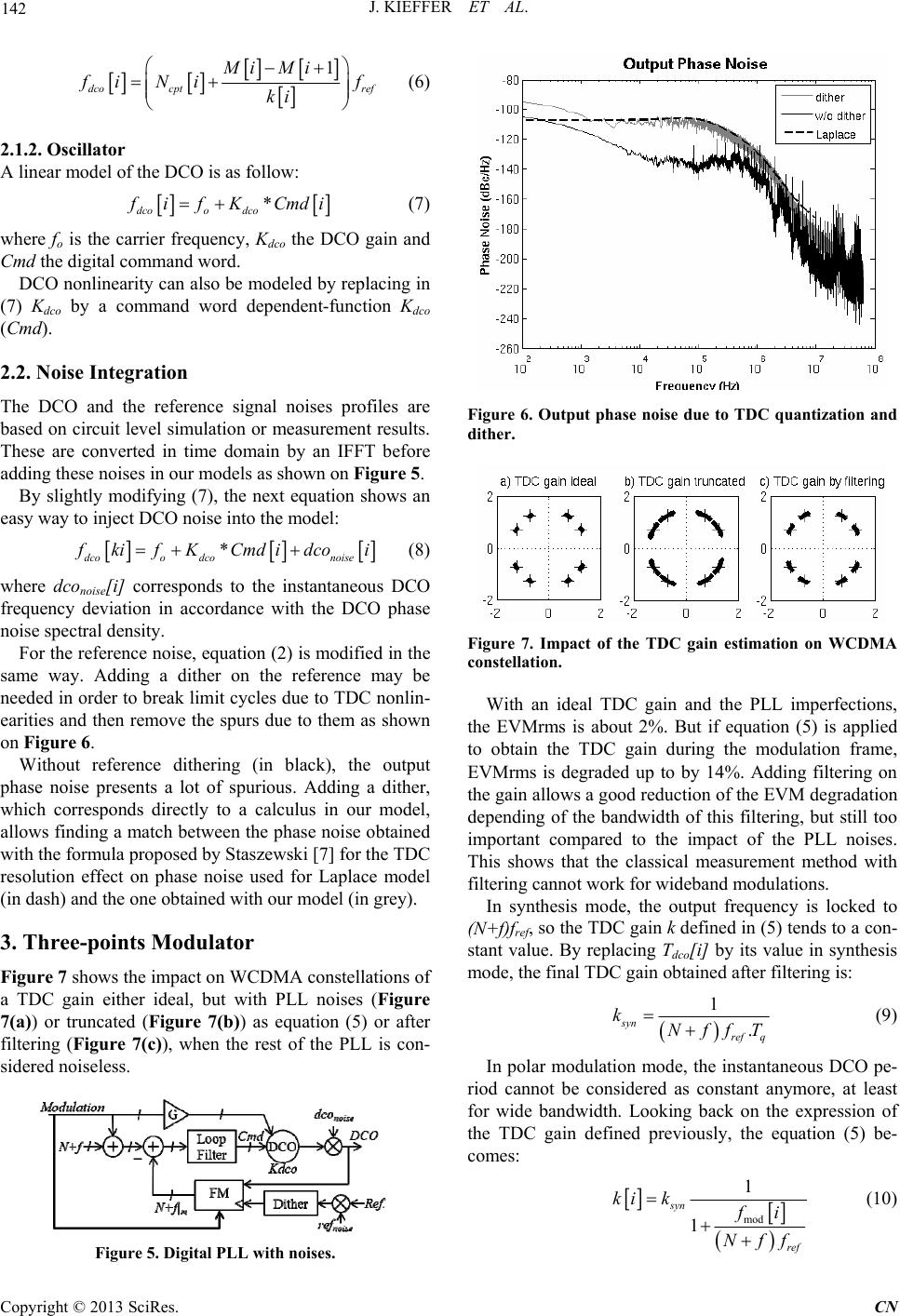 J. KIEFFER ET AL. 142 1 dco cptref Mi Mi f iNi f ki (6) 2.1.2. Oscillator A linear model of the DCO is as follow: * dcoo dco f ifK Cmdi (7) where fo is the carrier frequency, Kdco the DCO gain and Cmd the digital command word. DCO nonlinearity can also be modeled by replacing in (7) Kdco by a command word dependent-function Kdco (Cmd). 2.2. Noise Integration The DCO and the reference signal noises profiles are based on circuit level simulation or measurement results. These are converted in time domain by an IFFT before adding these noises in our models as shown on Figure 5. By slightly modifying (7), the next equation shows an easy way to inject DCO noise into the model: * dcoo dconoise f kifKCmd idcoi (8) where dconoise[i] corresponds to the instantaneous DCO frequency deviation in accordance with the DCO phase noise spectral density. For the reference noise, equation (2) is modified in the same way. Adding a dither on the reference may be needed in order to break limit cycles due to TDC nonlin- earities and then remove the spurs due to them as shown on Figure 6. Without reference dithering (in black), the output phase noise presents a lot of spurious. Adding a dither, which corresponds directly to a calculus in our model, allows finding a match between the phase noise obtained with the formula proposed by Staszewski [7] for the TDC resolution effect on phase noise used for Laplace model (in dash) and the one obtained with our model (in grey). 3. Three-points Modulator Figure 7 shows the impact on WCDMA constellations of a TDC gain either ideal, but with PLL noises (Figure 7(a)) or truncated (Figure 7(b)) as equation (5) or after filtering (Figure 7(c)), when the rest of the PLL is con- sidered noiseless. Figure 5. Digital P LL with noises . Figure 6. Output phase noise due to TDC quantization and dither. Figure 7. Impact of the TDC gain estimation on WCDMA constellation. With an ideal TDC gain and the PLL imperfections, the EVMrms is about 2%. But if equation (5) is applied to obtain the TDC gain during the modulation frame, EVMrms is degraded up to by 14%. Adding filtering on the gain allows a good reduction of the EVM degradation depending of the bandwidth of this filtering, but still too important compared to the impact of the PLL noises. This shows that the classical measurement method with filtering cannot work for wideband modulations. In synthesis mode, the output frequency is locked to (N+f)fref, so the TDC gain k defined in (5) tends to a con- stant value. By replacing Tdco[i] by its value in synthesis mode, the final TDC gain obtained after filtering is: 1 . syn ref q kNffT (9) In polar modulation mode, the instantaneous DCO pe- riod cannot be considered as constant anymore, at least for wide bandwidth. Looking back on the expression of the TDC gain defined previously, the equation (5) be- comes: mod 1 1 syn ref ki k f i Nff (10) Copyright © 2013 SciRes. CN 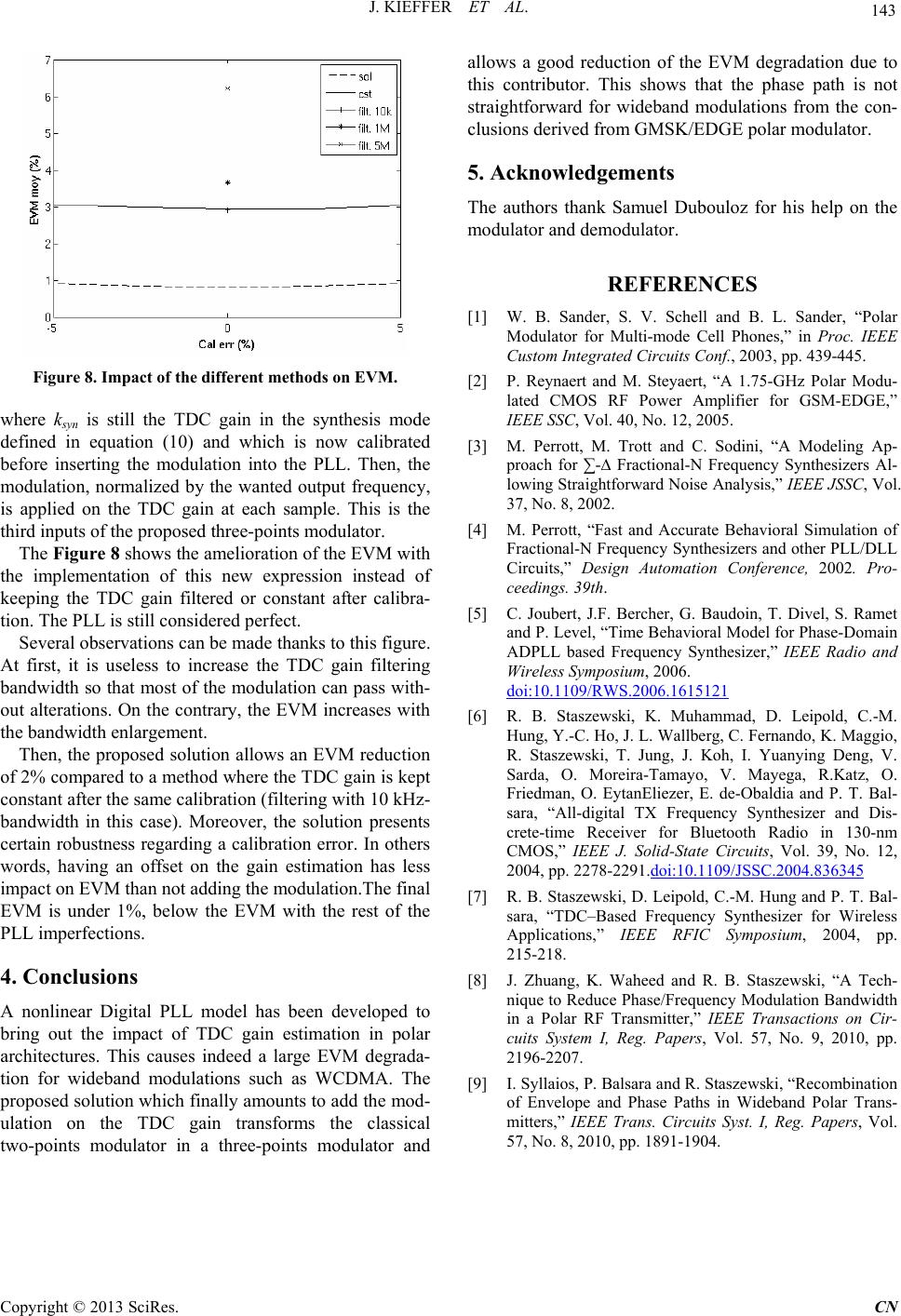 J. KIEFFER ET AL. Copyright © 2013 SciRes. CN 143 Figure 8. Impact of the different methods on EVM. where ksyn is still the TDC gain in the synthesis mode defined in equation (10) and which is now calibrated before inserting the modulation into the PLL. Then, the modulation, normalized by the wanted output frequency, is applied on the TDC gain at each sample. This is the third inputs of the proposed three-points modulator. The Figure 8 shows the amelioration of the EVM with the implementation of this new expression instead of keeping the TDC gain filtered or constant after calibra- tion. The PLL is still considered perfect. Several observations can be made thanks to this figure. At first, it is useless to increase the TDC gain filtering bandwidth so that most of the modulation can pass with- out alterations. On the contrary, the EVM increases with the bandwidth enlargement. Then, the proposed solution allows an EVM reduction of 2% compared to a method where the TDC gain is kept constant after the same calibration (filtering with 10 kHz- bandwidth in this case). Moreover, the solution presents certain robustness regarding a calibration error. In others words, having an offset on the gain estimation has less impact on EVM than not adding the modulation.The final EVM is under 1%, below the EVM with the rest of the PLL imperfections. 4. Conclusions A nonlinear Digital PLL model has been developed to bring out the impact of TDC gain estimation in polar architectures. This causes indeed a large EVM degrada- tion for wideband modulations such as WCDMA. The proposed solution which finally amounts to add the mod- ulation on the TDC gain transforms the classical two-points modulator in a three-points modulator and allows a good reduction of the EVM degradation due to this contributor. This shows that the phase path is not straightforward for wideband modulations from the con- clusions derived from GMSK/EDGE polar modulator. 5. Acknowledgements The authors thank Samuel Dubouloz for his help on the modulator and demodulator. REFERENCES [1] W. B. Sander, S. V. Schell and B. L. Sander, “Polar Modulator for Multi-mode Cell Phones,” in Proc. IEEE Custom Integrated Circuits Conf., 2003, pp. 439-445. [2] P. Reynaert and M. Steyaert, “A 1.75-GHz Polar Modu- lated CMOS RF Power Amplifier for GSM-EDGE,” IEEE SSC, Vol. 40, No. 12, 2005. [3] M. Perrott, M. Trott and C. Sodini, “A Modeling Ap- proach for ∑-∆ Fractional-N Frequency Synthesizers Al- lowing Straightforward Noise Analysis,” IEEE JSSC, Vol. 37, No. 8, 2002. [4] M. Perrott, “Fast and Accurate Behavioral Simulation of Fractional-N Frequency Synthesizers and other PLL/DLL Circuits,” Design Automation Conference, 2002. Pro- ceedings. 39th. [5] C. Joubert, J.F. Bercher, G. Baudoin, T. Divel, S. Ramet and P. Level, “Time Behavioral Model for Phase-Domain ADPLL based Frequency Synthesizer,” IEEE Radio and Wireless Symposium, 2006. doi:10.1109/RWS.2006.1615121 [6] R. B. Staszewski, K. Muhammad, D. Leipold, C.-M. Hung, Y.-C. Ho, J. L. Wallberg, C. Fernando, K. Maggio, R. Staszewski, T. Jung, J. Koh, I. Yuanying Deng, V. Sarda, O. Moreira-Tamayo, V. Mayega, R.Katz, O. Friedman, O. EytanEliezer, E. de-Obaldia and P. T. Bal- sara, “All-digital TX Frequency Synthesizer and Dis- crete-time Receiver for Bluetooth Radio in 130-nm CMOS,” IEEE J. Solid-State Circuits, Vol. 39, No. 12, 2004, pp. 2278-2291.doi:10.1109/JSSC.2004.836345 [7] R. B. Staszewski, D. Leipold, C.-M. Hung and P. T. Bal- sara, “TDC–Based Frequency Synthesizer for Wireless Applications,” IEEE RFIC Symposium, 2004, pp. 215-218. [8] J. Zhuang, K. Waheed and R. B. Staszewski, “A Tech- nique to Reduce Phase/Frequency Modulation Bandwidth in a Polar RF Transmitter,” IEEE Transactions on Cir- cuits System I, Reg. Papers, Vol. 57, No. 9, 2010, pp. 2196-2207. [9] I. Syllaios, P. Balsara and R. Staszewski, “Recombination of Envelope and Phase Paths in Wideband Polar Trans- mitters,” IEEE Trans. Circuits Syst. I, Reg. Papers, Vol. 57, No. 8, 2010, pp. 1891-1904. |