

Paper Menu >>
Journal Menu >>
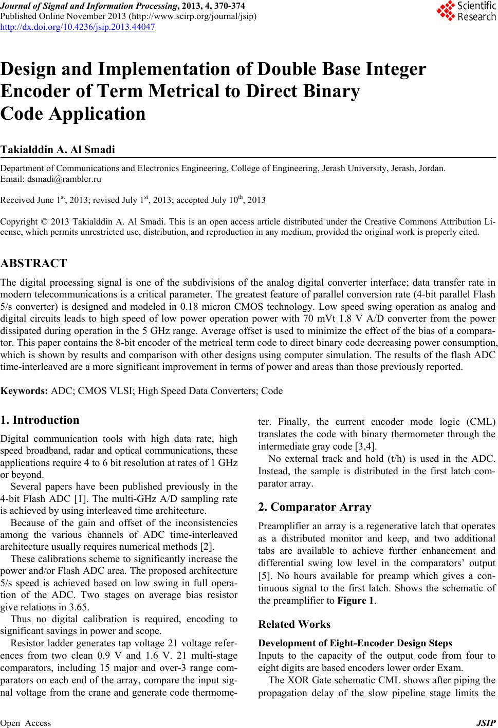 Journal of Signal and Information Processing, 2013, 4, 370-374 Published Online November 2013 (http://www.scirp.org/journal/jsip) http://dx.doi.org/10.4236/jsip.2013.44047 Open Access JSIP Design and Implementation of Double Base Integer Encoder of Term Metrical to Direct Binary Code Application Takialddin A. Al Smadi Department of Communications and Electronics Engineering, College of Engineering, Jerash University, Jerash, Jordan. Email: [email protected] Received June 1st, 2013; revised July 1st, 2013; accepted July 10th, 2013 Copyright © 2013 Takialddin A. Al Smadi. This is an open access article distributed under the Creative Commons Attribution Li- cense, which permits unrestricted use, distribution, and reproduction in any medium, provided the original work is properly cited. ABSTRACT The digital processing signal is one of the subdivisions of the analog digital converter interface; data transfer rate in modern telecommunications is a critical parameter. The greatest feature of parallel conversion rate (4-bit parallel Flash 5/s converter) is designed and modeled in 0.18 micron CMOS technology. Low speed swing operation as analog and digital circuits leads to high speed of low power operation power with 70 mVt 1.8 V A/D converter from the power dissipated during operation in the 5 GHz range. Average offset is used to minimize the effect of the bias of a compara- tor. This paper contains the 8-bit encoder of the metrical term code to direct binary code decreasing power consumption, which is shown by results and comparison with other designs using computer simulation. The results of the flash ADC time-interleaved are a more significant improvement in terms of power and areas than those previously reported. Keywords: ADC; CMOS VLSI; High Speed Data Converters; Code 1. Introduction Digital communication tools with high data rate, high speed broadband, radar and optical communications, these applications require 4 to 6 bit resolution at rates of 1 GHz or beyond. Several papers have been published previously in the 4-bit Flash ADC [1]. The multi-GHz A/D sampling rate is achieved by using interleaved time architecture. Because of the gain and offset of the inconsistencies among the various channels of ADC time-interleaved architecture usually requires numerical methods [2]. These calibrations scheme to significantly increase the power and/or Flash ADC area. The proposed architecture 5/s speed is achieved based on low swing in full opera- tion of the ADC. Two stages on average bias resistor give relations in 3.65. Thus no digital calibration is required, encoding to significant savings in power and scope. Resistor ladder generates tap voltage 21 voltage refer- ences from two clean 0.9 V and 1.6 V. 21 multi-stage comparators, including 15 major and over-3 range com- parators on each end of the array, compare the input sig- nal voltage from the crane and generate code thermome- ter. Finally, the current encoder mode logic (CML) translates the code with binary thermometer through the intermediate gray code [3,4]. No external track and hold (t/h) is used in the ADC. Instead, the sample is distributed in the first latch com- parator array. 2. Comparator Array Preamplifier an array is a regenerative latch that operates as a distributed monitor and keep, and two additional tabs are available to achieve further enhancement and differential swing low level in the comparators’ output [5]. No hours available for preamp which gives a con- tinuous signal to the first latch. Shows the schematic of the preamplifier to Figure 1. Related Works Development of Eight-Encoder Design Steps Inputs to the capacity of the output code from four to eight digits are based encoders lower order Exam. The XOR Gate schematic CML shows after piping the propagation delay of the slow pipeline stage limits the  Design and Implementation of Double Base Integer Encoder of Term Metrical to Direct Binary Code Application 371 operating frequency. So to implement an efficient sche- me of piping, it is desirable to have some delays at all stages [6]. Diagram of the encoder is shown in Figure 2 and de- veloped in accordance with prudent use of a minimum number of components, which reduces the space occu- pied by the on-chip. MOSFETs-substrate transistors with n-channel T1, T4 and T5 are connected to the negative rail power supply Vss, and the substrate p-MOSFETs with channel T2, T3 and T6 to the positive rail Vdd [7]. Encoder (Figure 2) consists of two CMOS—keys on the basis of transistors T1, T2 and T5, T6, which are con- trolled by the voltage at the input X1; Y0 determines the MSB output binary code. Input X1 comes from the output of the comparator switching threshold which corresponds to the middle of the two-digit range input ADC. Keys at the same switching voltage X0 and X2 from the outputs of the other two comparators to generate low-order output Y1 binary ADC. Based on the proposed scheme can be implemented three-bit encoder, where a block with two- digit designation DEC encoder according Proceeding si- milarly, we obtain a four-digit encoder circuit based on the three-digit encoder [8]. This requires the use of two- input multiplexers labeled MUX, Figure 3 shows its’ scheme. Substrate MOSFET with n-channel T2, T4, T5, T6, T8 and T10 are connected to the negative rail power supply Vss, and the substrate MOSFETs p-channel T1, T3, T7 and T9—to the positive rail Vdd. The multiplexer is a signal at the address input A. When the signal at input A, equal logical unit, the output signal from the input D1, and when the signal A, equal to a logical zero, with input D2. Inverters based on transistors T7 - T10 are the buffer elements. Thus, increasing the bit similar to Figure 3. Modeling was conducted with (tt, ss, ff, snfp, fnsp) for three values of temperatures −40˚C and 27˚C, 85˚C. The Figure 1. Schematic of the preamplifier. results are presented in Table 1. 3. Material and Methods Simulation Results Power characteristics of the encoder performed using MOSFETs Cadence Virtuoso based on 180 nm CMOS technology from UMC to 1.8 V single supply [9]. Delay time-shift eight-evaluated by the response of the encoder output LSB Y8 direct binary code when the input code in the thermometric all 255 bits of logic zero to logic one on the front, and vice versa trailing edge, due to the encoder circuit solution. According to the presented in the previ- ous section schemes, the most time-delay switch will have LSB output direct binary code. Clock frequency. Winning on the power consumption of circuit solutions presented encoder compared to known analogs [8-10] can evaluate on the basis of the simulation results. It is necessary to implement the conversion of power con- sumption being compared encoder (Pref) the equivalent Encoder, executed in the same way, 8-bit word length, manufactured in 180 nm CMOS technology and has a clock speed of 1 GHz. In this case, the supply current from the translation were held constant. Then the change in power consumption can be estimated: at another bit by the coefficient [9]. eqref bit Equivalent, and compares the encoder respectively, when changing technology—a factor NN e c E E. eq —voltage encoder, made in 180 nm CMOS tech- nology E 1. 8 В eq E, —encoder supply voltage ref E being compared; when the clock—e c F F , & eq ref F F—clock frequency equivalent to the developed and the compared encoders respectively. Then the equivalent power con- sumption is defined as 2. eq ref NN eq eq eqref ref ref EF Fp EF Table 2 under the conditions of winning based on es- timates of power consumption circuitry solutions devel- oped encoder compared to known analogs is table. The minimal gain in power consumption is obtained for eight-ADC encoder from Gain in power consumption is obtained for eight-ADC encoder from [10] 0.438 1.811.3 T 0.439 0.7 2 eq dev P P Pt—average power consumption of the developed en- coder. The maximum gain in power consumption is ob- tained for the encoder [11] on the basis of multiplexers. 0.254 145.3 T 0.449 0.1 eq dev P P Open Access JSIP  Design and Implementation of Double Base Integer Encoder of Term Metrical to Direct Binary Code Application Open Access JSIP 372 Figure 2. Implementation of encoder with four stage pipeline and only one type of gate. Figure 3. Eight-bit encoder.  Design and Implementation of Double Base Integer Encoder of Term Metrical to Direct Binary Code Application 373 Table 1. Consumption of the encoder. Terms T ˚C Time-delay switch Duration of the recessionFront time Power consumption −40 584 24 43 430 27 640 29 50 442 tt 85 689 32 55 461 −40 881 31 59 411 27 957 38 70 429 ss 85 1020 44 78 446 −40 431 19 33 446 27 475 23 39 460 ff 85 513 26 43 485 −40 666 24 44 469 27 726 29 51 483 snfp 85 778 34 56 504 −40 434 24 45 408 27 588 28 52 425 Snsp 85 634 23 58 443 Mean value 674 29 52 449 The maximum value 1020 44 78 504 Table 2. Decreased power c onsumption. Encoder CMOS Power consumption. (t) Full Adders 24.7 Memory Elements 41.6 Multiplexers 45.2 Logic Elements 0.18 1.4 4. Conclusion The paper proposed a circuit solution to thermometric encoder code in straight binary code. Eight-circuit simu- lation performed in CAD Cadence Virtuoso for 180 nm CMOS technology with a unipolar voltage 1.8 V. Maxi- mumly delayed time-shift is about 1 ns, which allows the use of the scheme in the processing of signals with a fre- quency of 1 GHz along with existing analogues. Average power consumption does not exceed 500 mW. All else being equal to a gain on the power consumption in com- parison, the known digital calibration can be added to implement ultra-high-speed time-interleaved ADCs to 40 times. The reduction in the number of comparators ar- chitecture makes it useful in portable ECG systems which operate at low voltage and low frequency range. REFERENCES [1] R. Yousry, E. Hegazi and H. F. Ragai, “A Third-Order 9-Bit 10-MHz CMOS Modulator with One Active Stage,” IEEE Transactions on Circuits and Systems I: Regular Papers, Vol. 55, No. 9, 2008, pp. 2469-2482. [2] C. Sandner, M. Clara, A. Santner, T. Hartig and F. Kuttner, “A 6-Bit 1.2-GS/s Low-Power Flash-ADC in 0.13 μm Di- gital CMOS,” IEEE Journal of Solid-State Circuits, Vol. 40, No. 7, 2005, pp. 1499-1505. [3] P. Nuzzo, P. Van Der Plas, G. De Bernardinis, R. Van Der Perre, L. Gyselinckx and B. Terreni, “A 10.6Mw/ 0.8Pj Power-Scalable 1Gs/S 4B Adc in 0.18/Spl Mu/M Cmos with 5.8Ghz Erbw,” The 43rd ACM/IEEE of the Design Automation Conference, San Francisco, 2006, pp. 873-878. [4] K. Uyttenhove and M. S. J. Steyaert, “A 1.8-V 6-Bit 1.3-Ghz Flash Adc in 0.25-ΜM Cmos,” IEEE Journal of Solid-State Circuits, Vol. 38, No. 7, 2003. [5] M. F. Chang, “Semiconductor Technology Considera- tions in High Speed Data Conversion,” IEEE of Com- pound Semiconductor Integ rated Circuit Symposium, 2004, pp. 31-34. [6] G. L. Madhumati, K. Ramakoteswara Rao and M. Mad- havilatha, “Comparison of 5-Bit Thermometer-to-Binary Decoders in 1.8 V, 0.18 μm CMOS Technology for Flash ADCs,” 2009 International Conference on Signal Proc- essing Systems, Singapore, 15-17 May 2009, pp. 516-520. [7] S. Sheikhaei, S. Mirabbasi and A. Ivanov, “An Encoder for a 5 GS/s 4-Bit Flash ADC in 0.18 μm CMOS,” Cana- dian Conference of the Electrical and Computer Engi- neering, May 2005, pp. 698-701. [8] T. A. Al Smadi, “Computer Application Using Low Cost Open Access JSIP  Design and Implementation of Double Base Integer Encoder of Term Metrical to Direct Binary Code Application 374 Smart Sensor,” International Journal of Computer Aided Engineering and Technology, Vol. 4, No. 6, 2012, pp. 567-579. http://dx.doi.org/10.1504/IJCAET.2012.049572 [9] Y. Lavania, G. T. Varghese and K. K. Mahapatra, “An Ultra Low Power Encoder for 5 Bit Flash ADC,” Interna- tional Conference on Emerging Trends in VLSI, Embed- ded System, Nano Electronics and Telecommunication System (ICEVENT), 2013, pp. 1-5. [10] M. S. Nguyen and J. Kim, “Design and Implementation of Double Base Integer Encoder in the Flash ADC,” The 6th International Conference on Electrical Engineering, Pattaya, 6-9 May 2009, pp. 496-499. [11] K. Uyttenhove and M. Steyaert, “Speed-Power-Accuracy Tradeoff in High-Speed CMOS ADCs,” IEEE Transac- tions on Circuits and Systems II: Analog and Digital Sig- nal Processing, Vol. 49, No. 4, pp. 280-287. http://dx.doi.org/10.1109/TCSII.2002.801191 Open Access JSIP |