

Paper Menu >>
Journal Menu >>
 Journal of Analytical Sciences, Methods and Instrumentation, 2013, 3, 152-157 http://dx.doi.org/10.4236/jasmi.2013.33018 Published Online September 2013 (http://www.scirp.org/journal/jasmi) The Basis for Design and Manufacture of a DSP-Based Coincidence Spectrometer Nguyen Xuan Hai1*, Pham Ngoc Tuan1, Nguyen Nhi Dien1, Dang Lanh1, Tuong Thi Thu Huong1, Pham Dinh Khang2 1Nuclear Research Institute, Dalat, Vietnam; 2Nuclear Training Center, Hanoi, Vietnam. Email: *[email protected] Received July 1st, 2013; revised August 8th, 2013; accepted August 17th, 2013 Copyright © 2013 Nguyen Xuan Hai et al. This is an open access article distributed under the Creative Commons Attribution Li- cense, which permits unrestricted use, distribution, and reproduction in any medium, provided the original work is properly cited. ABSTRACT The coincidence technique and the coincidence spectroscopy have been developed and applied for over 40 years. Most of popular coincidence measurement systems were based on analog electronics techniques such as time to amplitude conversion (TAC) or logic selecting coincidence unit. The above-mentioned systems are relatively cumbersome and complicated to use. With the strong growth of digital electronics techniques and computational science, the coincidence measurement systems will be constructed simpler but more efficient with the sake of application. This article presents the design principle and signal processing of a simple two-channel coincidence system by a technique of digital signal processing (DSP) using Field Programmable Gate Arrays (FPGA) devices at Nuclear Research Institute (NRI), Dalat. Keywords: Coincidence Spectrometer; Digital Signal Processing; FPGA 1. Introduction The background reduction measurement systems with active methods are based on coincidence or anti-coinci- dence techniques. They are mainly built from proper functional electronics modules in NIM or CAMAC stan- dards [1,2]. They allow us to identify coincidence or anti- coincidence events via main electronics blocks called coincidence unit or time to amplitude converter. Nor- mally, basic configuration of a coincidence measurement system will, at least, consist of two channels, and the selection of coincidence event pairs depends on the de- fining moment of the pulses appearing at “Timing” out- put of the pre-amplifier. Obvious drawback of this sys- tem is cumbersome in size, adjusting operation and syn- chronizing signals among electronics stages. The growth of computer engineering and programma- ble devices that are capable of operating at high frequen- cies has allowed us to design a new spectrometry genera- tion. The spectrometry generation is compact on size, simple in terms of connectivity and using [2-4]. At Nuclear Research Institute (NRI), Dalat, a number of researches and construction of Compton suppression as well as event-event coincidence systems were perfor- med in 1990s. The results of these studies were reported in [5]. In the recent period at NRI, further studies on the coincidence spectrometer were presented in several pub- lications [6-8]. Overall, although there have been sig- nificant improvements on acquiring as well as processing data, this system is still based on the traditional way in obtaining signals under the operation of a coincidence unit or TAC. With the research results gathered during the installation, investigation and exploitation of an “event-event” coincidence spectrometer on digital signal processing (DSP) at NRI, we have now proposed a new approach for a design of the DSP-based multi-application coincidence technique through Field Programmable Gate Arrays (FPGA) devices. The basis for the design of this spectrometer will be presented within the framework of this article. 2. The Basis and Method for the Design 2.1. Design of Multi-Channel Analyzer The block diagram of MCA is presented in Figure 1. The functions of the diagram can be summarized as follows: The pre-filter works as high-pass filter giving an out- put signal with a constant shaping time. In addition, the pre-filter has amplification function to generate the ap- propriate signals for ADC conversion. The pre-filter’ output signals are sent to flash ADC for *Corresponding author. Copyright © 2013 SciRes. JASMI 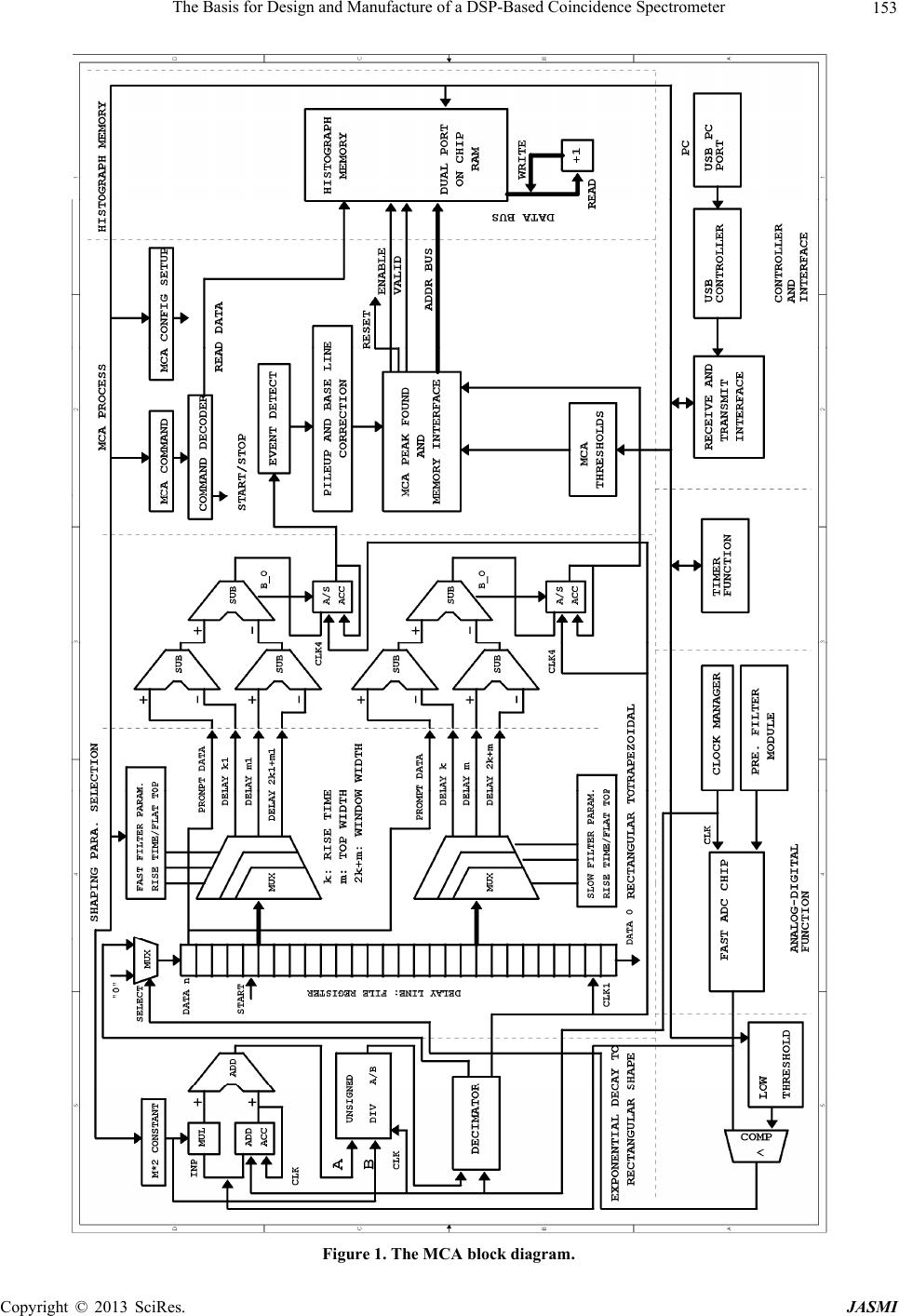 The Basis for Design and Manufacture of a DSP-Based Coincidence Spectrometer 153 Figure 1. The MCA block diagram. Copyright © 2013 SciRes. JASMI  The Basis for Design and Manufacture of a DSP-Based Coincidence Spectrometer 154 sampling. The ADC’ output signals are digital copies of input’ analog signals. The transfering “Exponential Decay to Rectangular Shape” circuit converts exponential decay to rectangular pulse, and its function is the opposite of high pass de- convoler (HPD). The transfering “Rectangular Shape to Trapezoidal Shape” circuit converts shape of rectangular to trapezoidal pulse, and its function is the low pass filter (LPF). The circuits of pulse pile-up rejection, base line restoration and built-in configuration are also designed in the main board. The pulse pile-up rejection circuit detects the pile-up pulses in duration from rise time to half of the flat width, in slow channel. In case of non-overlapped pulse is de- tected in monitoring duration, the right pulse will be analysis. A dual port memory is integrated in FPGA de- vice for buffering data. The preset time is set by user with capacity up to 4.2 × 10⁹ seconds. The interface cir- cuit is integrated in the main board and connected to PC through a USB-RS232 bridge. 2.2. Design of the “Event-Event” Coincidence Spectrometer The block diagram of the “event-event” coincidence spectrometer is presented in Figure 2. According to the block diagram, the coincidence spectrometer consists of three parts; they are two DSP-based multi-channel ana- lyzers and one channel of timing discriminators. Two MCA channels are used for getting the energy spectrum from the two detectors. Timing discrimination circuits are used for the time interval measurement. The pre-filter, Fast ADC and DSP MCA are the components of the en- ergy analysis channel. The FAST COMPARATOR, TIME COUNTER, TIME COMPARATOR and COIN- CIDENT CONTROLLER are the components of the coincidence channel. Except for the PRE-FILTER, FAST ADC and DDR2 MEMORY, almost other components are designed and integrated into one FPGA device which is named XC6SLX16. Figure 2. The block diagram of the “event-event” coinci- dence spectrometer. The external DDR2 MEMORY is used to save the measured results. The interface circuit is integrated on the main board and connected to PC through USB-RS232 bridge. Principal Operation Two MCAs receive pulses from the preamplifier’s en- ergy outputs, the pulses’ amplitudes are analyzed (by DSP techniques); simultaneously, the preamplifier’s output pulses are connected to fast comparator circuits. The output signals of these comparator circuits are used to start/stop a time counter. The used clock frequency is 400 MHz (2.5 ns period). The contents of the counter (time interval between two events) are compared with values of preset time interval; if the measured time is in the selected range, the amplitudes of pair of events will be recorded. Three values E1, E2 and T will be stored into memory; in which E1 and E2 are energy values of pair of coincidence gamma rays, and T is time interval. The measured results are read by data acquisition pro- gram and saved to file on the hard disk. 3. Fabricating 3.1. Hardware The entire design is programmed and configured in the FPGA chip XC6LX16-CS324. The used main board is SP601 kit supplied by Xilinx as Figure 3. 3.2. Data Acquisition Program The data acquisition program for energy and timing spectra was written under LabWIEW 8.5. The functions of program are as follows: + Connecting peripheral devices to PC and interfacing to PC through USB port. + Control of data acquisition for multi-MCA mode: start/stop data acquisition, preset measurement time, data saving… + Control of data acquisition for “event-event” coin- cidence mode: start/stop data acquisition, preset meas- urement time, data saving… + The base data analysis: display spectra, counts per channel, energy calibration, zoom in and zoom out spec- tra. 3.3. The Main Features of Spectroscopy 1) The multi-channel analysis: - Input: accept the preamplifier’s output pulses from semiconductor detector, the amplitude from tens to 500 mV; - Resolution: 8192 channels; - Capacity of counts/channel: 232 − 1; - Preset time capacity: 232 − 1 seconds with 1 second Copyright © 2013 SciRes. JASMI  The Basis for Design and Manufacture of a DSP-Based Coincidence Spectrometer 155 Figure 3. The main board. step; - The integral nonlinearity: <±0.05%; - Shaping time: 0.4; 0.8; 1.6; 3.2; 6.4; 12.6; 25.2 μs; - Coarse gain: 1, 2, 5 and 10; - Fine gain: 0.75 ÷ 1.25, step 0.01; - Displaying and rejecting the pile-up pulses, baseline correction and dead time correction. 2) Event-event coincidence: - Preset coincidence time window: 5 ÷ 10,000 ns, res- olution step 5 ns; - Mode: coincidence, PHA; - Memory capacity: 16 M events. 3) Power supply: +12 V/800 mA, −12 V/50 mA, +6 V/300 mA, −6 V/100 mA. 4) Dimensions: width NIM 2M. 4. Testing and Results The experiment configuration is showed in Figure 4. The disk-shaped 60Co source with activity of 24 kBq was placed between the two detectors (GMX35). The dis- tance from source to the detectors’ surfaces was 4 cm. In front of each detector, a sheet of lead 2 mm in thickness Figure 4. Experiment configuration. was placed to reduce the effect of back scattering from the detectors to each other. Data were collected during 2 h. The interfacing pro- gram was set up in event-event coincidence mode. The data files were saved to hard disk automatically in all 4096 coincidence events. The Figures 5-7 are energy spectra of each channel, summation spectra and timing spectra respectively. Figure 6 shows the 60Co summation spectra, with only one peak and Compton scattering background. The coin- cident spectrum (Figure 5) of each channel contains two Copyright © 2013 SciRes. JASMI 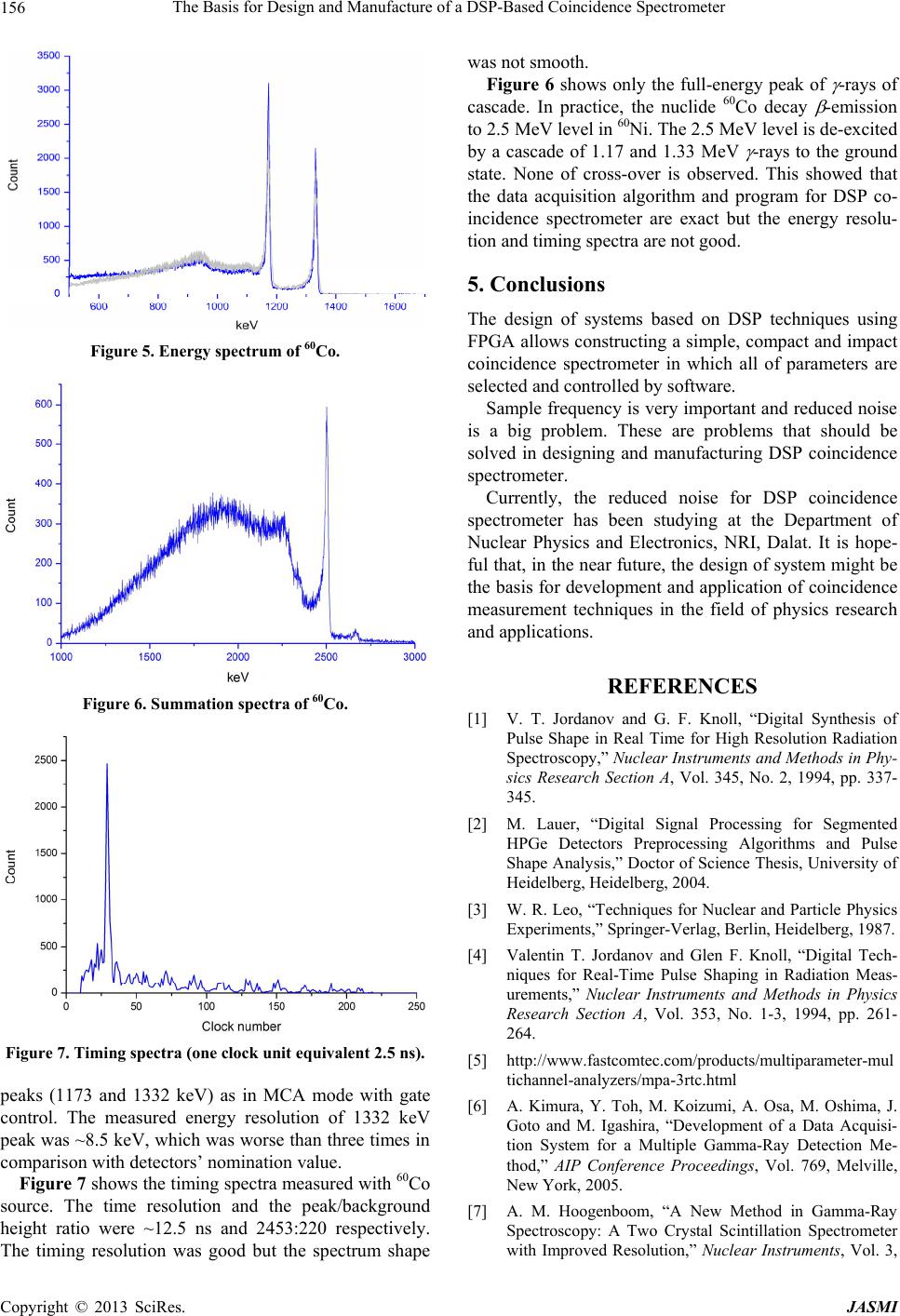 The Basis for Design and Manufacture of a DSP-Based Coincidence Spectrometer 156 Figure 5. Energy spectrum of 60Co. Figure 6. Summation spectra of 60Co. Figure 7. Timing spectra (one clock unit equivalent 2.5 ns). peaks (1173 and 1332 keV) as in MCA mode with gate control. The measured energy resolution of 1332 keV peak was ~8.5 keV, which was worse than three times in comparison with detectors’ nomination value. Figure 7 shows the timing spectra measured with 60Co source. The time resolution and the peak/background height ratio were ~12.5 ns and 2453:220 respectively. The timing resolution was good but the spectrum shape was not smooth. Figure 6 shows only the full-energy peak of -rays of cascade. In practice, the nuclide 60Co decay -emission to 2.5 MeV level in 60Ni. The 2.5 MeV level is de-excited by a cascade of 1.17 and 1.33 MeV -rays to the ground state. None of cross-over is observed. This showed that the data acquisition algorithm and program for DSP co- incidence spectrometer are exact but the energy resolu- tion and timing spectra are not good. 5. Conclusions The design of systems based on DSP techniques using FPGA allows constructing a simple, compact and impact coincidence spectrometer in which all of parameters are selected and controlled by software. Sample frequency is very important and reduced noise is a big problem. These are problems that should be solved in designing and manufacturing DSP coincidence spectrometer. Currently, the reduced noise for DSP coincidence spectrometer has been studying at the Department of Nuclear Physics and Electronics, NRI, Dalat. It is hope- ful that, in the near future, the design of system might be the basis for development and application of coincidence measurement techniques in the field of physics research and applications. REFERENCES [1] V. T. Jordanov and G. F. Knoll, “Digital Synthesis of Pulse Shape in Real Time for High Resolution Radiation Spectroscopy,” Nucle ar Instruments and Methods in Phy- sics Research Section A, Vol. 345, No. 2, 1994, pp. 337- 345. [2] M. Lauer, “Digital Signal Processing for Segmented HPGe Detectors Preprocessing Algorithms and Pulse Shape Analysis,” Doctor of Science Thesis, University of Heidelberg, Heidelberg, 2004. [3] W. R. Leo, “Techniques for Nuclear and Particle Physics Experiments,” Springer-Verlag, Berlin, Heidelberg, 1987. [4] Valentin T. Jordanov and Glen F. Knoll, “Digital Tech- niques for Real-Time Pulse Shaping in Radiation Meas- urements,” Nuclear Instruments and Methods in Physics Research Section A, Vol. 353, No. 1-3, 1994, pp. 261- 264. [5] http://www.fastcomtec.com/products/multiparameter-mul tichannel-analyzers/mpa-3rtc.html [6] A. Kimura, Y. Toh, M. Koizumi, A. Osa, M. Oshima, J. Goto and M. Igashira, “Development of a Data Acquisi- tion System for a Multiple Gamma-Ray Detection Me- thod,” AIP Conference Proceedings, Vol. 769, Melville, New York, 2005. [7] A. M. Hoogenboom, “A New Method in Gamma-Ray Spectroscopy: A Two Crystal Scintillation Spectrometer with Improved Resolution,” Nuclear Instruments, Vol. 3, Copyright © 2013 SciRes. JASMI  The Basis for Design and Manufacture of a DSP-Based Coincidence Spectrometer Copyright © 2013 SciRes. JASMI 157 No. 2, 1958, pp. 57-68. doi:10.1016/0369-643X(58)90092-6 [8] A. Pullia, “Quasi-Optimum Gamma and X-Ray Spectros- copy Based on Real-Time Digital Techniques,” Nuclear Instruments and Methods in Physics Research A, Vol. 439, No. 2-3, 2000, pp. 378-384. doi:10.1016/S0168-9002(99)00897-9 |