

Paper Menu >>
Journal Menu >>
 Circuits and Systems, 2013, 4, 387-392 http://dx.doi.org/10.4236/cs.2013.45051 Published Online September 2013 (http://www.scirp.org/journal/cs) Practical and User-Friendly Circuits and System Design for Signals’ Sensing and Generation Ching-Hwa Ho1*, Ji-Hsien Ho2 1Graduate Institute of Applied Science and Technology, National Taiwan University of Science and Technology, Taipei, Taiwan 2Media and Visual Communication, Department of Industrial Design, Chang Gung University, Tao-Yaun, Taiwan Email: *[email protected] Received July 6, 2013; revised August 6, 2013; accepted August 13, 2013 Copyright © 2013 Ching-Hwa Ho, Ji-Hsien Ho. This is an open access article distributed under the Creative Commons Attribution License, which permits unrestricted use, distribution, and reproduction in any medium, provided the original work is properly cited. ABSTRACT Design and implementation of a personal computer (PC) based measurement circuits & system that containing signals’ sensing and generation are demonstrated in this study. The instrument can be easily operated via a user-friendly inter- face consisted of some functional keys displayed on the PC screen. Compact design of the hardware for the two units (signals’ sensing and generation) is made in a plug-in style of PC input/output (I/O) card so that no extra space for the instrument is needed. Design concepts for the hardware and software of the instrument are described. Functional per- formances of the setup of signals’ sensing and generation are tested. The results show user-friendly function and well- behaved performance for the package design. Keywords: A/D Conversion; D/A Conversion; Data Acquisition; I/O Interface Cards; Auto-Testing Equipment 1. Introduction The apparatuses of signals’ sensing (SS) and generation (SG) are important equipments for testing analog and digital signals in laboratory. The electrical engineers usually need a good sensing and monitor tool to analyze electrical signals they want to measure. A practical sens- ing and monitor tool must support many useful functions such as data storage, computer linking, numeric analysis, and curve printing to meet different demands by users. To match the fundamental requirements, a SS device must be computerized because numeric data processing and data storage are the essential functions for users. Furthermore, the experimentalists in laboratory usually require a proper SG device to generate some specific functional signals for testing. A practical SG device should generate not only the basic functions of sine, tri- angle, and square waves but also the signal with a user- defined waveform. To generate user-defined waveforms, a fully computerized SG is necessary to be developed. From the experimentalists’ point of view, a fully compu- terized auto-testing-equipment (ATE) that combining both SS and SG apparatuses should be essential in ful- filling their experimental testing tasks. A personal computer (PC) based ATE is now a very convenient instrumentation system. The PC-based SS device had ever been utilized for studying nonvolatile memories [1], for simulating virtual spectrum analyzer, imitating digital image processor [2,3], and checking the function of high-frequency power electronics [4]. The functions of PC-controlled SG can be a waveform gen- erator [1], a programmable constant current source to generate electroluminescences from optoelectronic de- vices [5], and for generation of timing clocks to drive linear charge-coupled-device (CCD) arrays [5,6]. Al- though the individual SS or SG device had ever been found, a systematic study on overall understanding of the actual design and implementation of electronic hardware and software of a PC auxiliary ATE would be valuable to be announced herein. In this paper, practical design and implementation of a real ATE measurement package are demonstrated (i.e. system diagram as shown in Figure 1). The instrument is easily operated via some user-friendly functional keys displayed on the PC screen. The hardware for the SS and SG is fabricated in a plug-in style of PC I/O card so that no extra instrumentation space is needed. The sampling frequency of the SS card can be programmably setting by user. The maximum sampling rate is up to 19 MHz. The *Corresponding author. C opyright © 2013 SciRes. CS 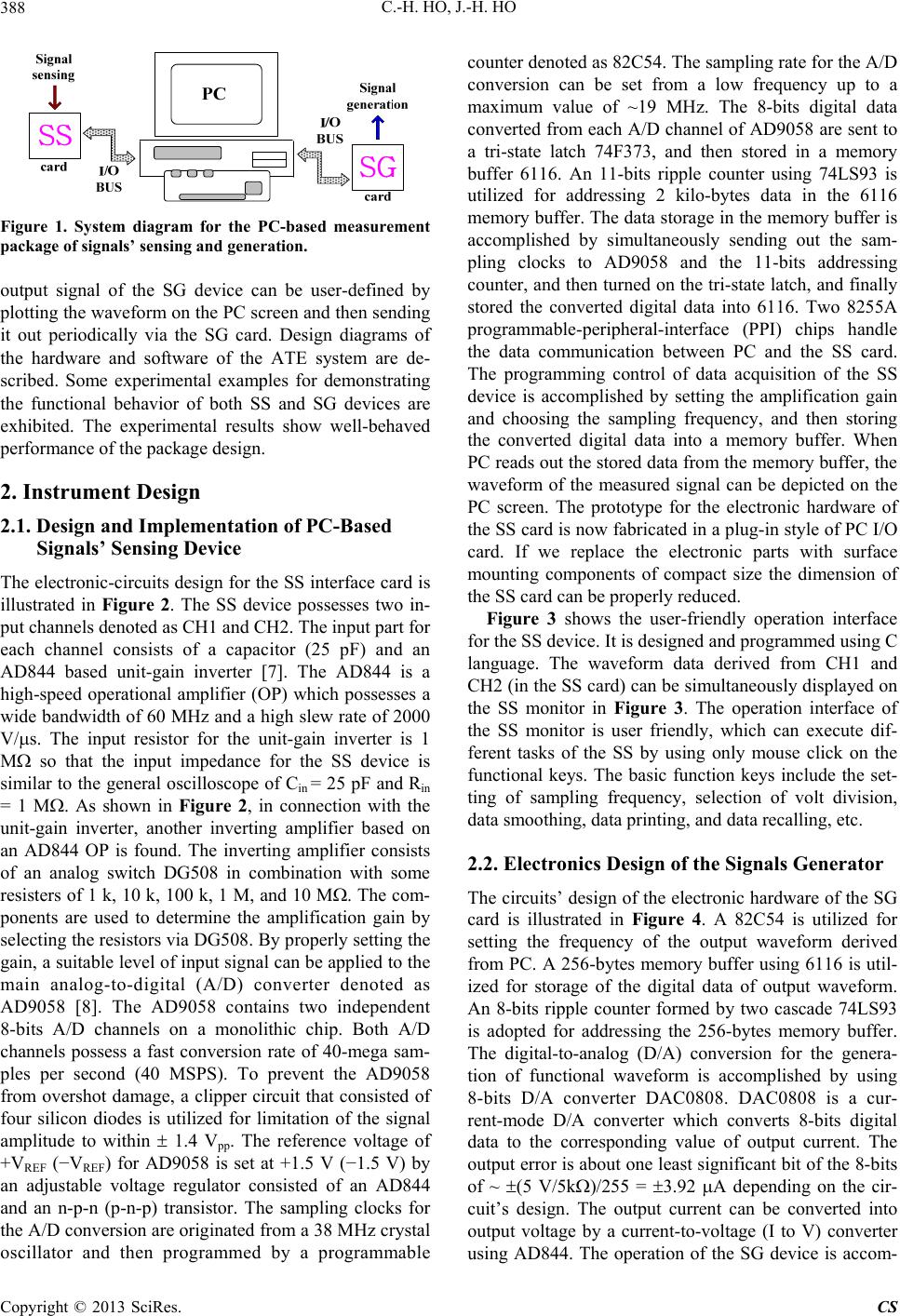 C.-H. HO, J.-H. HO 388 Figure 1. System diagram for the PC-based measurement package of signals’ sensing and generation. output signal of the SG device can be user-defined by plotting the waveform on the PC screen and then sending it out periodically via the SG card. Design diagrams of the hardware and software of the ATE system are de- scribed. Some experimental examples for demonstrating the functional behavior of both SS and SG devices are exhibited. The experimental results show well-behaved performance of the package design. 2. Instrument Design 2.1. Design and Implementation of PC-Based Signals’ Sensing Device The electronic-circuits design for the SS interface card is illustrated in Figure 2. The SS device possesses two in- put channels denoted as CH1 and CH2. The input part for each channel consists of a capacitor (25 pF) and an AD844 based unit-gain inverter [7]. The AD844 is a high-speed operational amplifier (OP) which possesses a wide bandwidth of 60 MHz and a high slew rate of 2000 V/s. The input resistor for the unit-gain inverter is 1 M so that the input impedance for the SS device is similar to the general oscilloscope of Cin = 25 pF and Rin = 1 M. As shown in Figure 2, in connection with the unit-gain inverter, another inverting amplifier based on an AD844 OP is found. The inverting amplifier consists of an analog switch DG508 in combination with some resisters of 1 k, 10 k, 100 k, 1 M, and 10 M. The com- ponents are used to determine the amplification gain by selecting the resistors via DG508. By properly setting the gain, a suitable level of input signal can be applied to the main analog-to-digital (A/D) converter denoted as AD9058 [8]. The AD9058 contains two independent 8-bits A/D channels on a monolithic chip. Both A/D channels possess a fast conversion rate of 40-mega sam- ples per second (40 MSPS). To prevent the AD9058 from overshot damage, a clipper circuit that consisted of four silicon diodes is utilized for limitation of the signal amplitude to within 1.4 Vpp. The reference voltage of +VREF (−VREF) for AD9058 is set at +1.5 V (−1.5 V) by an adjustable voltage regulator consisted of an AD844 and an n-p-n (p-n-p) transistor. The sampling clocks for the A/D conversion are originated from a 38 MHz crystal oscillator and then programmed by a programmable counter denoted as 82C54. The sampling rate for the A/D conversion can be set from a low frequency up to a maximum value of ~19 MHz. The 8-bits digital data converted from each A/D channel of AD9058 are sent to a tri-state latch 74F373, and then stored in a memory buffer 6116. An 11-bits ripple counter using 74LS93 is utilized for addressing 2 kilo-bytes data in the 6116 memory buffer. The data storage in the memory buffer is accomplished by simultaneously sending out the sam- pling clocks to AD9058 and the 11-bits addressing counter, and then turned on the tri-state latch, and finally stored the converted digital data into 6116. Two 8255A programmable-peripheral-interface (PPI) chips handle the data communication between PC and the SS card. The programming control of data acquisition of the SS device is accomplished by setting the amplification gain and choosing the sampling frequency, and then storing the converted digital data into a memory buffer. When PC reads out the stored data from the memory buffer, the waveform of the measured signal can be depicted on the PC screen. The prototype for the electronic hardware of the SS card is now fabricated in a plug-in style of PC I/O card. If we replace the electronic parts with surface mounting components of compact size the dimension of the SS card can be properly reduced. Figure 3 shows the user-friendly operation interface for the SS device. It is designed and programmed using C language. The waveform data derived from CH1 and CH2 (in the SS card) can be simultaneously displayed on the SS monitor in Figure 3. The operation interface of the SS monitor is user friendly, which can execute dif- ferent tasks of the SS by using only mouse click on the functional keys. The basic function keys include the set- ting of sampling frequency, selection of volt division, data smoothing, data printing, and data recalling, etc. 2.2. Electronics Design of the Signals Generator The circuits’ design of the electronic hardware of the SG card is illustrated in Figure 4. A 82C54 is utilized for setting the frequency of the output waveform derived from PC. A 256-bytes memory buffer using 6116 is util- ized for storage of the digital data of output waveform. An 8-bits ripple counter formed by two cascade 74LS93 is adopted for addressing the 256-bytes memory buffer. The digital-to-analog (D/A) conversion for the genera- tion of functional waveform is accomplished by using 8-bits D/A converter DAC0808. DAC0808 is a cur- rent-mode D/A converter which converts 8-bits digital data to the corresponding value of output current. The output error is about one least significant bit of the 8-bits of ~ (5 V/5k)/255 = 3.92 A depending on the cir- cuit’s design. The output current can be converted into output voltage by a current-to-voltage (I to V) converter using AD844. The operation of the SG device is accom- Copyright © 2013 SciRes. CS 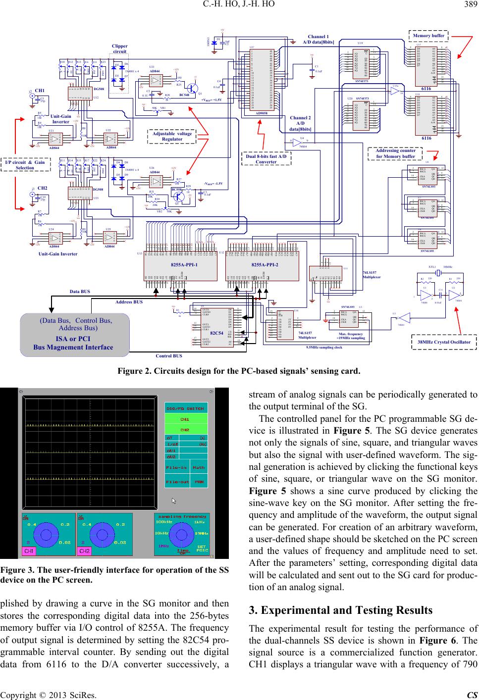 C.-H. HO, J.-H. HO Copyright © 2013 SciRes. CS 389 R0(1) 2 R0(2) 3 CKA 14 QA 12 CKB 1 QB 9 QC 8 QD 11 U5 D0 8 OUT0 10 D1 7 GATE0 11 D2 6 CLK0 9 D3 5 D4 4 D5 3 D6 2 OUT1 13 D7 1 GATE1 14 CLK1 15 CS 21 RD 22 WR 23 OUT2 17 A0 19 GATE2 16 A1 20 CLK2 18 U9 82C54 G 15 A/B 1 1A 2 1B 31Y 4 2A 5 2B 6 2Y 7 3A 11 3B 10 3Y 9 4A 14 4B 13 4Y 12 U10 G 15 A/ B 1 1A 2 1B 3 1Y 4 2A 5 2B 6 2Y 7 3A 11 3B 10 3Y 9 4A 14 4B 13 4Y 12 U11 R3 1k 34 33 32 31 30 29 28 27 4 3 2 1 40 39 38 37 18 19 20 21 22 23 24 25 14 15 16 17 13 12 11 10 5 36 9 8 35 6 8255A-PPI-2 D0 34 D1 33 D2 32 D3 31 D4 30 D5 29 D6 28 D7 27 PA0 4PA1 3PA2 2PA3 1PA4 40 PA5 39 PA6 38 PA7 37 PB0 18 PB1 19 PB2 20 PB3 21 PB4 22 PB5 23 PB6 24 PB7 25 PC0 14 PC1 15 PC2 16 PC3 17 PC4 13 PC5 12 PC6 11 PC7 10 RD 5 WR 36 A0 9 A1 8 RESET 35 CS 6 U13 8255A-PPI-1 R0(1) 2 R0(2) 3 CKA 14 QA 12 CKB 1 QB 9 QC 8 QD 11 U6 R0(1) 2 R0(2) 3 CKA 14 QA 12 CKB 1 QB 9 QC 8 QD 11 U7 R0(1) 2 R0(2) 3 CKA 14 QA 12 CKB 1 QB 9 QC 8 QD 11 U8 SN74LS93 A0 8 A1 7 A2 6 A3 5 A4 4 A5 3 A6 2 A7 1 A8 23 A9 22 A10 19 18 20 21 D0 9 D1 10 D2 11 D3 13 D4 14 D5 15 D6 16 D7 17 U17 A0 8 A1 7 A2 6 A3 5 A4 4 A5 3 A6 2 A7 1 A8 23 A9 22 A10 19 E18 G20 W21 D0 9 D1 10 D2 11 D3 13 D4 14 D5 15 D6 16 D7 17 U18 6116 U15a OC 1 C11 1D 3 1Q 2 2D 4 2Q 5 3D 7 3Q 6 4D 8 4Q 9 5D 13 5Q 12 6D 14 6Q 15 7D 17 7Q 16 8D 18 8Q 19 U19 SN74F373 OC 1 C11 1D 3 1Q 2 2D 4 2Q 5 3D 7 3Q 6 4D 8 4Q 9 5D 13 5Q 12 6D 14 6Q 15 7D 17 7Q 16 8D 18 8Q 19 U20 SN74F373 C1 0.1uF vcc 5pF C2 D1 1N4001 -5V C5 25p U21 AD844 R4 1M R5 1M +12V R8 10K DG508 U12 R10 1 K R12 10 K R13 10 K R16 100 K R18 1M R23 10M U22 AD844 vcc U23 AD844 vcc R25 150 R28 10 Q1 BC548 +12V VR150K +5 D2 D3 Q2 BC558 vcc 32 33 34 35 36 37 38 39 40 41 42 43 44 45 46 47 481 2 3 4 5 6 7 8 9 10 11 12 13 14 15 16 17 18 19 20 21 22 23 24 25 26 27 28 29 30 31 U27 AD9058 -12V -12V +12V C2 0.1U C10 25p U24 AD844 R6 1M R7 1M +12V R9 10K 12 34 56 78 910 1112 1314 1516 DG508 U23 R11 1 K R14 10 K R15 10 K R17 100 K R22 1M R24 10M 1 2 3 4 5 6 7 8 U25 AD844 vcc U26 AD844 +12V R30 20K R31 20K vcc VR2 50K -12V D4 D5 -12V -12V +12V C3 0.1uF R27 150 -5V R29 10 C4 0.1uF -12V vcc D6 1N4001 x 4 D7 D8 1N4001 x 4 D9 89 U4 74S04 10 11 a0 a1 a2 a3 a4 a5 a6 a7 a8 a9 a10 a0 a1 a2 a3 a4 a5 a6 a7 a8 a9 a0 a1 a2 a3 a4 a5 a6 a7 a8 a9 a10 c0 c1 c2 c3 c4 c5 c6 c7 D0 D1 D2 D3 D4 D5 D6 D7 j2 CH1 j3 CH2 r3 r2 r1 s1 s2 s3 s1 s2 s3 r1 r2 r3 (Data Bus,Control Bus, Address Bus) ISA or PCI Bus Magnement Interface PA0 PA1 PA2 PA3 PA4 PA5 PA6 PA7 PB0 PB1 PB2 PB3 PB4 PB5 PB6 PB7 PC0 PC1 PC2 PC3 PC4 PC5 PC6 PC7 U12 D0 D1 D2 D3 D4 D5 D6 D7 RD WR A0 A1 RESET CS 6116 Data BUS Control BUS Address BUS 12 34 56 78 12 34 56 78 12 34 56 78 12 34 56 78 12 34 56 78 12 34 56 78 910 1112 1314 1516 Channel 2 A/D data[8bits] Channel 1 A/D data[8bits] SN74LS93 SN74LS93 SN74LS93 74LS157 E G W Max. frequency =19MHz sampling 9.5MHz sampling clock Multiplexer Addressing counter for Memory buffer Memory buffer Dual 8-bits fast A/D Converter Adjustable voltage Regulator I/P circuit & Gain Selection +VREF= +1.5V 74LS157 Multiplexer Unit-Gain Inverter Unit-Gain Inverter a10 Clipper circuit -VREF= -1.5V XTL1 38MHz U2 74S04 U1 74S04 R1 220 R2 220 U3 74S04 4 8 3 12 9 C11 0.01uF 38MHz Crystal Oscillator Figure 2. Circuits design for the PC-based signals’ sensing card. Figure 3. The user-friendly interface for operation of the SS device on the PC screen. plished by drawing a curve in the SG monitor and then stores the corresponding digital data into the 256-bytes memory buffer via I/O control of 8255A. The frequency of output signal is determined by setting the 82C54 pro- grammable interval counter. By sending out the digital data from 6116 to the D/A converter successively, a stream of analog signals can be periodically generated to the output terminal of the SG. The controlled panel for the PC programmable SG de- vice is illustrated in Figure 5. The SG device generates not only the signals of sine, square, and triangular waves but also the signal with user-defined waveform. The sig- nal generation is achieved by clicking the functional keys of sine, square, or triangular wave on the SG monitor. Figure 5 shows a sine curve produced by clicking the sine-wave key on the SG monitor. After setting the fre- quency and amplitude of the waveform, the output signal can be generated. For creation of an arbitrary waveform, a user-defined shape should be sketched on the PC screen and the values of frequency and amplitude need to set. After the parameters’ setting, corresponding digital data will be calculated and sent out to the SG card for produc- tion of an analog signal. 3. Experimental and Testing Results The experimental result for testing the performance of the dual-channels SS device is shown in Figure 6. The signal source is a commercialized function generator. CH1 displays a triangular wave with a frequency of 790  C.-H. HO, J.-H. HO 390 Vcc 13 Iout 4 msbA1 5 Vrf(-) 15 A2 6 A3 7 Vrf(+) 14 A4 8 A5 9 A6 10 COMP 16 A7 11 lsbA8 12 Vee 3 U9 DAC0808 D0 34 D1 33 D2 32 D3 31 D4 30 D5 29 D6 28 D7 27 PA0 4 PA1 3 PA2 2 PA3 1 PA4 40 PA5 39 PA6 38 PA7 37 PB0 18 PB1 19 PB2 20 PB3 21 PB4 22 PB5 23 PB6 24 PB7 25 PC014 PC115 PC216 PC317 PC413 PC512 PC611 PC710 RD 5 WR 36 A0 9 A1 8 RESET 35 CS 6 U1 8255A-PPI D0 8OUT0 10 D1 7GATE0 11 D2 6CLK0 9 D3 5 D4 4 D5 3 D6 2OUT1 13 D7 1GATE114 CLK1 15 CS 21 RD 22 WR 23 OUT2 17 A0 19 GATE216 A1 20 CLK2 18 U2 82C54 Q0 12 Q1 9Q2 8Q3 11 MR1 2 MR2 3 CLK0 14 CLK1 1 U6 74LS93 Q0 12 Q1 9Q2 8Q3 11 MR1 2 MR2 3 CLK0 14 CLK1 1 U7 74LS93 A0 2 A1 3 A2 4 A3 5 A4 6 A5 7 A6 8 A7 9 B0 18 B1 17 B2 16 B3 15 B4 14 B5 13 B6 12 B7 11 E 19 DIR 1 U8 74LS245 1A 2 1B 31Y 4 2A 5 2B 62Y 7 3A 11 3B 10 3Y 9 4A 14 4B 13 4Y 12 A/B 1 G 15 U4 74LS157 D0 3Q0 2 D1 4Q1 5 D2 7Q2 6 D3 8Q3 9 D4 13 Q4 12 D5 14 Q5 15 D6 17 Q6 16 D7 18 Q7 19 OE 1 LE 11 U3 74LS373 A0 8 A1 7 A2 6 A3 5 A4 4 A5 3 A6 2 A7 1 A8 23 A9 22 A10 19 E 18 G 20 W 21 D0 9 D1 10 D2 11 D3 13 D4 14 D5 15 D6 16 D7 17 U5 SRAM 6116 3 2 6 1 5 74 U10 AD844 3 2 6 1 5 74 U11 AD844 (Data Bus,Control Bus, Address Bus) PCI Bus Magnement Interface R1 1.3k R2 1k R3 10k R55k R4 2.5k C1 30pF -12 +5 +5 Counter CLEAR R6 1k +5 CLK -12 -12 +12 +12 OUT Data BUS Control BUS Address BUS D/A & I to V Converter 256 Byte Data Buffer Figure 4. Circuits design for the electronic hardware of the signal generator. Figure 5. The user-friendly PC interface for the operation of SG on the PC screen. Hz and amplitude of 1.8 Vpp. The values of frequency and amplitude are determined from the horizontal and vertical scales of the SS monitor. The sampling fre- quency for the data acquisition is 100 kHz. The voltage scale is 0.4 V. The observed dc offset for the triangular wave is zero. CH2 shows a square wave with frequency of 2.1 kHz and amplitude of 3 Vpp. The period (T = 0.00048 sec.) and frequency (1/T = 2.1 e + 03 Hz) of Figure 6. Experimental results of the programmable SS device. The signal sources are deduced from a 790-Hz tri- angular wave of 1.8 Vpp and a 2.1-kHz square wave of 3 Vpp. the square wave is determined by setting a time window using two moveable straight lines displayed on the SS screen. Sampling frequencies of 1 k, 10 k, 100 k, and 1 MHz can be chosen from the SS monitor. The maximum sampling rate can be set up to 19 MHz. Figure 7 shows a square wave measured by the maximum sampling fre- quency of 19 MHz. The amplitude is 5 Vpp, duty cycle is Copyright © 2013 SciRes. CS 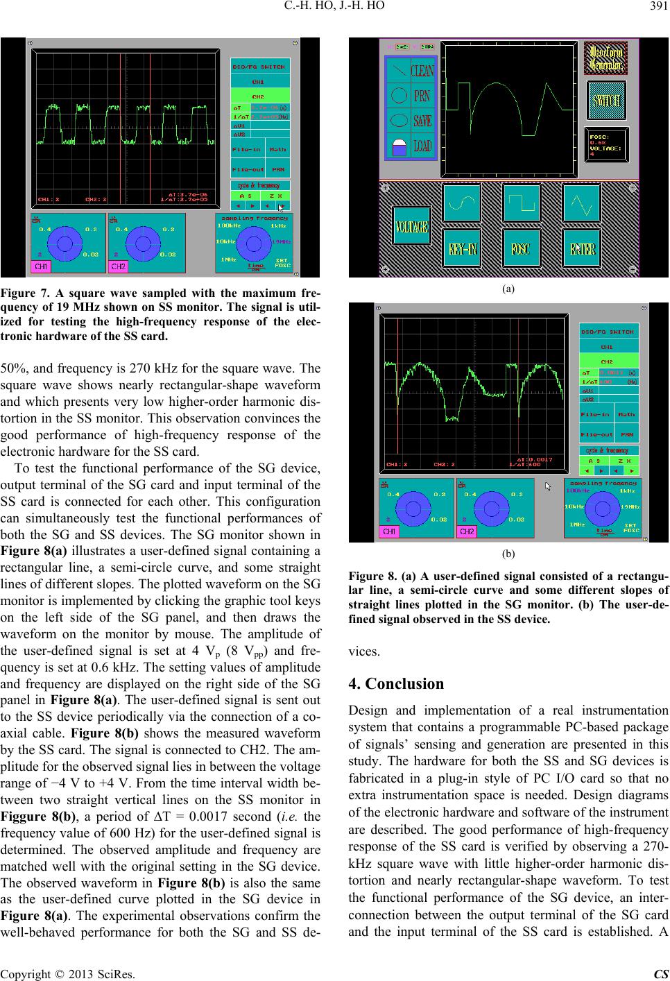 C.-H. HO, J.-H. HO 391 Figure 7. A square wave sampled with the maximum fre- quency of 19 MHz shown on SS monitor. The signal is util- ized for testing the high-frequency response of the elec- tronic hardware of the SS card. 50%, and frequency is 270 kHz for the square wave. The square wave shows nearly rectangular-shape waveform and which presents very low higher-order harmonic dis- tortion in the SS monitor. This observation convinces the good performance of high-frequency response of the electronic hardware for the SS card. To test the functional performance of the SG device, output terminal of the SG card and input terminal of the SS card is connected for each other. This configuration can simultaneously test the functional performances of both the SG and SS devices. The SG monitor shown in Figure 8(a) illustrates a user-defined signal containing a rectangular line, a semi-circle curve, and some straight lines of different slopes. The plotted waveform on the SG monitor is implemented by clicking the graphic tool keys on the left side of the SG panel, and then draws the waveform on the monitor by mouse. The amplitude of the user-defined signal is set at 4 Vp (8 Vpp) and fre- quency is set at 0.6 kHz. The setting values of amplitude and frequency are displayed on the right side of the SG panel in Figure 8(a). The user-defined signal is sent out to the SS device periodically via the connection of a co- axial cable. Figure 8(b) shows the measured waveform by the SS card. The signal is connected to CH2. The am- plitude for the observed signal lies in between the voltage range of −4 V to +4 V. From the time interval width be- tween two straight vertical lines on the SS monitor in Figgure 8(b), a period of T = 0.0017 second (i.e. the frequency value of 600 Hz) for the user-defined signal is determined. The observed amplitude and frequency are matched well with the original setting in the SG device. The observed waveform in Figure 8(b) is also the same as the user-defined curve plotted in the SG device in Figure 8(a). The experimental observations confirm the well-behaved performance for both the SG and SS de- (a) (b) Figure 8. (a) A user-defined signal consisted of a rectangu- lar line, a semi-circle curve and some different slopes of straight lines plotted in the SG monitor. (b) The user-de- fined signal observed in the SS device. vices. 4. Conclusion Design and implementation of a real instrumentation system that contains a programmable PC-based package of signals’ sensing and generation are presented in this study. The hardware for both the SS and SG devices is fabricated in a plug-in style of PC I/O card so that no extra instrumentation space is needed. Design diagrams of the electronic hardware and software of the instrument are described. The good performance of high-frequency response of the SS card is verified by observing a 270- kHz square wave with little higher-order harmonic dis- tortion and nearly rectangular-shape waveform. To test the functional performance of the SG device, an inter- connection between the output terminal of the SG card and the input terminal of the SS card is established. A Copyright © 2013 SciRes. CS 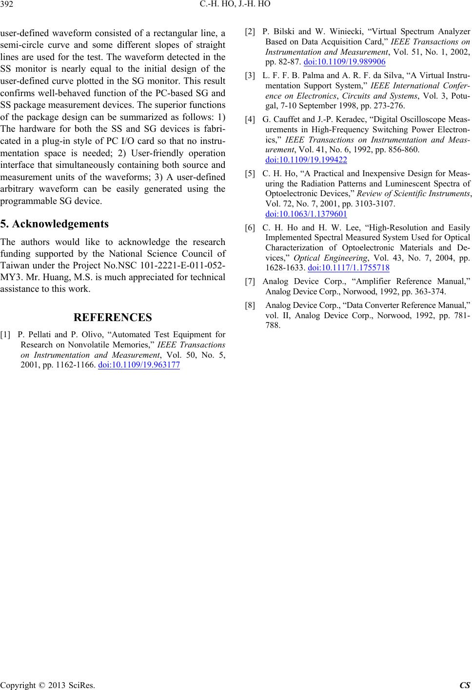 C.-H. HO, J.-H. HO Copyright © 2013 SciRes. CS 392 user-defined waveform consisted of a rectangular line, a semi-circle curve and some different slopes of straight lines are used for the test. The waveform detected in the SS monitor is nearly equal to the initial design of the user-defined curve plotted in the SG monitor. This result confirms well-behaved function of the PC-based SG and SS package measurement devices. The superior functions of the package design can be summarized as follows: 1) The hardware for both the SS and SG devices is fabri- cated in a plug-in style of PC I/O card so that no instru- mentation space is needed; 2) User-friendly operation interface that simultaneously containing both source and measurement units of the waveforms; 3) A user-defined arbitrary waveform can be easily generated using the programmable SG device. 5. Acknowledgements The authors would like to acknowledge the research funding supported by the National Science Council of Taiwan under the Project No.NSC 101-2221-E-011-052- MY3. Mr. Huang, M.S. is much appreciated for technical assistance to this work. REFERENCES [1] P. Pellati and P. Olivo, “Automated Test Equipment for Research on Nonvolatile Memories,” IEEE Transactions on Instrumentation and Measurement, Vol. 50, No. 5, 2001, pp. 1162-1166. doi:10.1109/19.963177 [2] P. Bilski and W. Winiecki, “Virtual Spectrum Analyzer Based on Data Acquisition Card,” IEEE Transactions on Instrumentation and Measurement, Vol. 51, No. 1, 2002, pp. 82-87. doi:10.1109/19.989906 [3] L. F. F. B. Palma and A. R. F. da Silva, “A Virtual Instru- mentation Support System,” IEEE International Confer- ence on Electronics, Circuits and Systems, Vol. 3, Potu- gal, 7-10 September 1998, pp. 273-276. [4] G. Cauffet and J.-P. Keradec, “Digital Oscilloscope Meas- urements in High-Frequency Switching Power Electron- ics,” IEEE Transactions on Instrumentation and Meas- urement, Vol. 41, No. 6, 1992, pp. 856-860. doi:10.1109/19.199422 [5] C. H. Ho, “A Practical and Inexpensive Design for Meas- uring the Radiation Patterns and Luminescent Spectra of Optoelectronic Devices,” Review of Scientific Instruments, Vol. 72, No. 7, 2001, pp. 3103-3107. doi:10.1063/1.1379601 [6] C. H. Ho and H. W. Lee, “High-Resolution and Easily Implemented Spectral Measured System Used for Optical Characterization of Optoelectronic Materials and De- vices,” Optical Engineering, Vol. 43, No. 7, 2004, pp. 1628-1633. doi:10.1117/1.1755718 [7] Analog Device Corp., “Amplifier Reference Manual,” Analog Device Corp., Norwood, 1992, pp. 363-374. [8] Analog Device Corp., “Data Converter Reference Manual,” vol. II, Analog Device Corp., Norwood, 1992, pp. 781- 788. |