

Paper Menu >>
Journal Menu >>
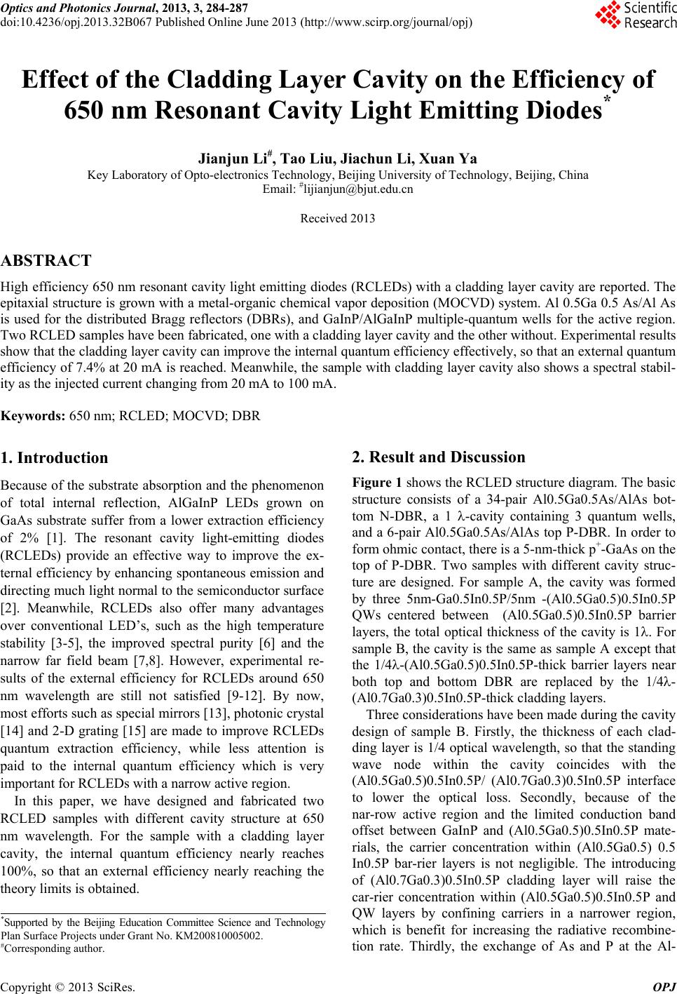 Optics and Photonics Journal, 2013, 3, 284-287 doi:10.4236/opj.2013.32B067 Published Online June 2013 (http://www.scirp.org/journal/opj) Effect of the Cladding Layer Cavity on the Efficiency of 650 nm Resonant Cavity Light Emitting Diodes* Jianjun Li#, Tao Liu, Jiachun Li, Xuan Ya Key Laboratory of Opto-electronics Technology, Beijing University of Technology, Beijing, China Email: #[email protected] Received 2013 ABSTRACT High efficiency 650 nm resonant cavity light emitting diodes (RCLEDs) with a cladding layer cavity are reported. The epitaxial structure is grown with a metal-organic chemical vapor deposition (MOCVD) system. Al 0.5Ga 0.5 As/Al As is used for the distributed Bragg reflectors (DBRs), and GaInP/AlGaInP multiple-quantum wells for the active region. Two RCLED samples have been fabricated, one with a cladding layer cavity and the other without. Experimental results show that the cladding layer cavity can improve the internal quantum efficiency effectively, so that an external quantum efficiency of 7.4% at 20 mA is reached. Meanwhile, the sample with cladding layer cavity also shows a spectral stabil- ity as the injected current changing from 20 mA to 100 mA. Keywords: 650 nm; RCLED; MOCVD; DBR 1. Introduction Because of the substrate absorption and the phenomenon of total internal reflection, AlGaInP LEDs grown on GaAs substrate suffer from a lower extraction efficiency of 2% [1]. The resonant cavity light-emitting diodes (RCLEDs) provide an effective way to improve the ex- ternal efficiency by enhancing spontaneous emission and directing much light normal to the semiconductor surface [2]. Meanwhile, RCLEDs also offer many advantages over conventional LED’s, such as the high temperature stability [3-5], the improved spectral purity [6] and the narrow far field beam [7,8]. However, experimental re- sults of the external efficiency for RCLEDs around 650 nm wavelength are still not satisfied [9-12]. By now, most efforts such as special mirrors [13], photonic crystal [14] and 2-D grating [15] are made to improve RCLEDs quantum extraction efficiency, while less attention is paid to the internal quantum efficiency which is very important for RCLEDs with a narrow active region. In this paper, we have designed and fabricated two RCLED samples with different cavity structure at 650 nm wavelength. For the sample with a cladding layer cavity, the internal quantum efficiency nearly reaches 100%, so that an external efficiency nearly reaching the theory limits is obtained. 2. Result and Discussion Figure 1 shows the RCLED structure diagram. The basic structure consists of a 34-pair Al0.5Ga0.5As/AlAs bot- tom N-DBR, a 1 -cavity containing 3 quantum wells, and a 6-pair Al0.5Ga0.5As/AlAs top P-DBR. In order to form ohmic contact, there is a 5-nm-thick p+-GaAs on the top of P-DBR. Two samples with different cavity struc- ture are designed. For sample A, the cavity was formed by three 5nm-Ga0.5In0.5P/5nm -(Al0.5Ga0.5)0.5In0.5P QWs centered between (Al0.5Ga0.5)0.5In0.5P barrier layers, the total optical thickness of the cavity is 1. For sample B, the cavity is the same as sample A except that the 1/4-(Al0.5Ga0.5)0.5In0.5P-thick barrier layers near both top and bottom DBR are replaced by the 1/4- (Al0.7Ga0.3)0.5In0.5P-thick cladding layers. Three considerations have been made during the cavity design of sample B. Firstly, the thickness of each clad- ding layer is 1/4 optical wavelength, so that the standing wave node within the cavity coincides with the (Al0.5Ga0.5)0.5In0.5P/ (Al0.7Ga0.3)0.5In0.5P interface to lower the optical loss. Secondly, because of the nar-row active region and the limited conduction band offset between GaInP and (Al0.5Ga0.5)0.5In0.5P mate- rials, the carrier concentration within (Al0.5Ga0.5) 0.5 In0.5P bar-rier layers is not negligible. The introducing of (Al0.7Ga0.3)0.5In0.5P cladding layer will raise the car-rier concentration within (Al0.5Ga0.5)0.5In0.5P and QW layers by confining carriers in a narrower region, which is benefit for increasing the radiative recombine- tion rate. Thirdly, the exchange of As and P at the Al- *Supported by the Beijing Education Committee Science and Technolog y Plan Surface Projects under Grant No. KM200810005002. #Corresponding author. Copyright © 2013 SciRes. OPJ 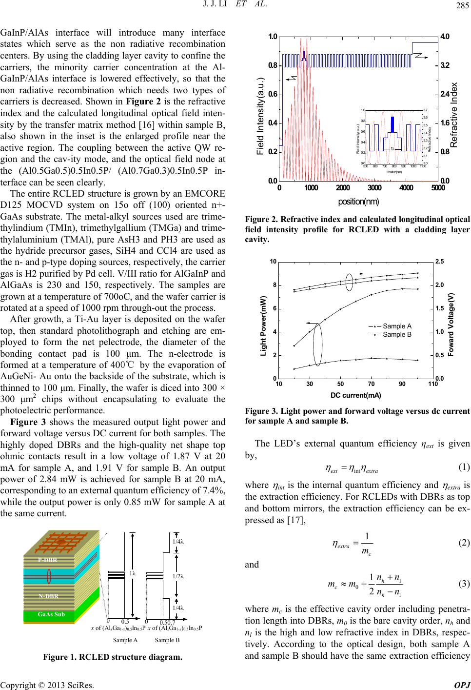 J. J. LI ET AL. 285 GaInP/AlAs interface will introduce many interface states which serve as the non radiative recombination centers. By using the cladding layer cavity to confine the carriers, the minority carrier concentration at the Al- GaInP/AlAs interface is lowered effectively, so that the non radiative recombination which needs two types of carriers is decreased. Shown in Figure 2 is the refractive index and the calculated longitudinal optical field inten- sity by the transfer matrix method [16] within sample B, also shown in the inset is the enlarged profile near the active region. The coupling between the active QW re- gion and the cav-ity mode, and the optical field node at the (Al0.5Ga0.5)0.5In0.5P/ (Al0.7Ga0.3)0.5In0.5P in- terface can be seen clearly. The entire RCLED structure is grown by an EMCORE D125 MOCVD system on 15o off (100) oriented n+- GaAs substrate. The metal-alkyl sources used are trime- thylindium (TMIn), trimethylgallium (TMGa) and trime- thylaluminium (TMAl), pure AsH3 and PH3 are used as the hydride precursor gases, SiH4 and CCl4 are used as the n- and p-type doping sources, respectively, the carrier gas is H2 purified by Pd cell. V/III ratio for AlGaInP and AlGaAs is 230 and 150, respectively. The samples are grown at a temperature of 700oC, and the wafer carrier is rotated at a speed of 1000 rpm through-out the process. After growth, a Ti-Au layer is deposited on the wafer top, then standard photolithograph and etching are em- ployed to form the net pelectrode, the diameter of the bonding contact pad is 100 μm. The n-electrode is formed at a temperature of 400℃ by the evaporation of AuGeNi- Au onto the backside of the substrate, which is thinned to 100 μm. Finally, the wafer is diced into 300 × 300 μm2 chips without encapsulating to evaluate the photoelectric performance. Figure 3 shows the measured output light power and forward voltage versus DC current for both samples. The highly doped DBRs and the high-quality net shape top ohmic contacts result in a low voltage of 1.87 V at 20 mA for sample A, and 1.91 V for sample B. An output power of 2.84 mW is achieved for sample B at 20 mA, corresponding to an external quantum efficiency of 7.4%, while the output power is only 0.85 mW for sample A at the same current. x of (Al x Ga 1-x ) 0.5 In 0.5 P 0 0.5 1 Sample A 0 0.5 0.7 1/4 1/4 1/2 Sample B x of (Al x Ga 1-x ) 0.5 In 0.5 P GaAs Sub N-DBR P-DBR Figure 1. RCLED structure diagram. 01000 2000 3000 4000 5000 0.0 0.8 1.6 2.4 3.2 4.0 0.0 0.2 0.4 0.6 0.8 1.0 500 600 700 800 90010001100 0. 0 0. 2 0. 4 0. 6 0. 8 1. 0 3.0 3.1 3.2 3.3 3.4 3.5 3.6 3.7 Refractive Index position(nm) Field Intensity(a.u.) Posi t i on( nm) Field Intensity(a.u.) Refractive Index 1 Figure 2. Refractive index and calculated longitudi nal optical field intensity profile for RCLED with a cladding layer cavity. 10 30 50 70 90110 0.0 0.5 1.0 1.5 2.0 2.5 0 2 4 6 8 10 Foward Voltage(V) Sample A Sample B DC current(mA) Light Power(mW) Figure 3. Light power and forward voltage versus dc current for sample A and sample B. The LED’s external quantum efficiency ηext is given by, int ext extra (1) where int is the internal quantum efficiency and extra is the extraction efficiency. For RCLEDs with DBRs as top and bottom mirrors, the extraction efficiency can be ex- pressed as [17], 1 extra c m (2) and 1 0 1 1 2 h c h nn mm nn (3) where mc is the effective cavity order including penetra- tion length into DBRs, m0 is the bare cavity order, nh and nl is the high and low refractive index in DBRs, respec- tively. According to the optical design, both sample A and sample B should have the same extraction efficiency Copyright © 2013 SciRes. OPJ 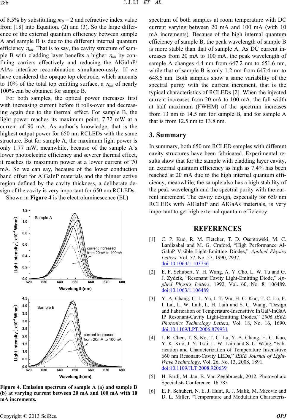 J. J. LI ET AL. 286 of 8.5% by substituting m0 = 2 and refractive index value from [18] into Equation. (2) and (3). So the large differ- ence of the external quantum efficiency between sample A and sample B is due to the different internal quantum efficiency int. That is to say, the cavity structure of sam- ple B with cladding layer benefits a higher int by con- fining carriers effectively and reducing the AlGaInP/ AlAs interface recombination simultaneo-ussly. If we have considered the opaque top electrode, which amounts to 10% of the total top emitting surface, a int of nearly 100% can be obtained for sample B. For both samples, the optical power increases first with increasing current before it rolls-over and decreas- ing again due to the thermal effect. For sample B, the light power reaches its maximum point, 7.72 mW at a current of 90 mA. As author’s knowledge, that is the highest output power for 650 nm RCLEDs with the same structure. But for sample A, the maximum light power is only 1.77 mW, meanwhile, because of the sample A’s lower photoelectric efficiency and severer thermal effect, it reaches its maximum power at a lower current of 70 mA. So we can say, because of the lower conduction band offset for AlGaInP materials and the thinner active region defined by the cavity thickness, a deliberate de- sign of the cavity is very important for 650 nm RCLEDs. Shown in Figure 4 is the electroluminescence (EL) 620 630 640650 660 670 680 0.0 0.2 0.4 0.6 0.8 1.0 1.2 Sample A Light Intensity( x10-4 W/nm) Wavelength(nm) current increased from 20mA to 100mA 620 630 640 650 660 670 680 0.0 0.5 1.0 1.5 2.0 2.5 3.0 3.5 4.0 4.5 Light Intensity( x10-4 W/nm) Wavelength(nm) Sample B current increased from 20mA to 100mA Figure 4. Emission spectrum of sample A (a) and sample B (b) at varying current between 20 mA and 100 mA with 10 mA increments. spectrum of both samples at room temperature with DC current varying between 20 mA and 100 mA (with 10 mA increments). Because of the high internal quantum efficiency of sample B, the peak wavelength of sample B is more stable than that of sample A. As DC current in- creases from 20 mA to 100 mA, the peak wavelength of sample A changes 4.4 nm from 647.2 nm to 651.6 nm, while that of sample B is only 1.2 nm from 647.4 nm to 648.6 nm. Both samples show a same variability of the spectral purity with the current increment, that is the typical characteristics of RCLEDs [2]. When the injected current increases from 20 mA to 100 mA, the full width at half maximum (FWHM) of the spectrum increases from 13 nm to 14.5 nm for sample B, and for sample A that is from 12.5 nm to 13.8 nm. 3. Summary In summary, both 650 nm RCLED samples with different cavity structures have been fabricated. Experimental re- sults show that for the sample with cladding layer cavity, an external quantum efficiency as high as 7.4% has been reached at 20 mA due to the high internal quantum effi- ciency, meanwhile, the sample also has a high stability of the peak wavelength and the spectral purity with the cur- rent increment. The cavity design, especially for 650 nm RCLEDs with AlGaInP and AlGaAs materials, is very important to get high external quantum efficiency. REFERENCES [1] C. P. Kuo, R. M. Fletcher, T. D. Osentowski, M. C. Lardizabal and M. G. Craford, “High Performance Al- GalnP Visible Light-Emitting Diodes,” Applied Physics Letters. Vol. 57, No. 27, 1990, 2937. doi:10.1063/1.103736 [2] E. F. Schubert, Y. H. Wang, A. Y. Cho, L. W. Tu and G. J. Zydzik, “Resonant Cavity Light-Emitting Diode,” Ap- plied Physics Letters, 1992, Vol. 60, No. 8, 106489. doi:10.1063/1.106489 [3] Y. A. Chang, C. L. Yu, I. T. Wu, H. C. Kuo, T. C. Lu, F. I. Lai, L. W. Laih, L. H. Laih and S. C. Wang, “Design and Fabrication of Temperature-Insensitive InGaP-InGaA IP Resonant-Cavity Light-Emitting Diodes,” 2006 IEEE Photonics Technology Letters, Vol. 18, No. 16, 1690. doi:10.1109/LPT.2006.879931 [4] J. R. Chen, T. S. Ko, T. C. Lu, Y. A. Chang, H. C. Kuo, Y. K. Kuo, J. Y. Tsai, L. W. Laih and S. C. Wang, “Fab- rication and Characterization of Temperature Insensitive 660 nm Resonant-Cavity LEDs,” IEEE Journal of Light- Wave Technology, Vol. 26, No. 13, 2008, 1891. doi:10.1109/JLT.2008.920639 [5] H. Fardi, M. Jan, B. Van Zeghbroeck, 2012, Photovoltaic Specialists Conference. 16 785 [6] E. F. Schubert, N. E. J. Hunt, R. J. Malik, M. Micovic and D. L. Miller, “Temperature and Modulation Characteris- Copyright © 2013 SciRes. OPJ 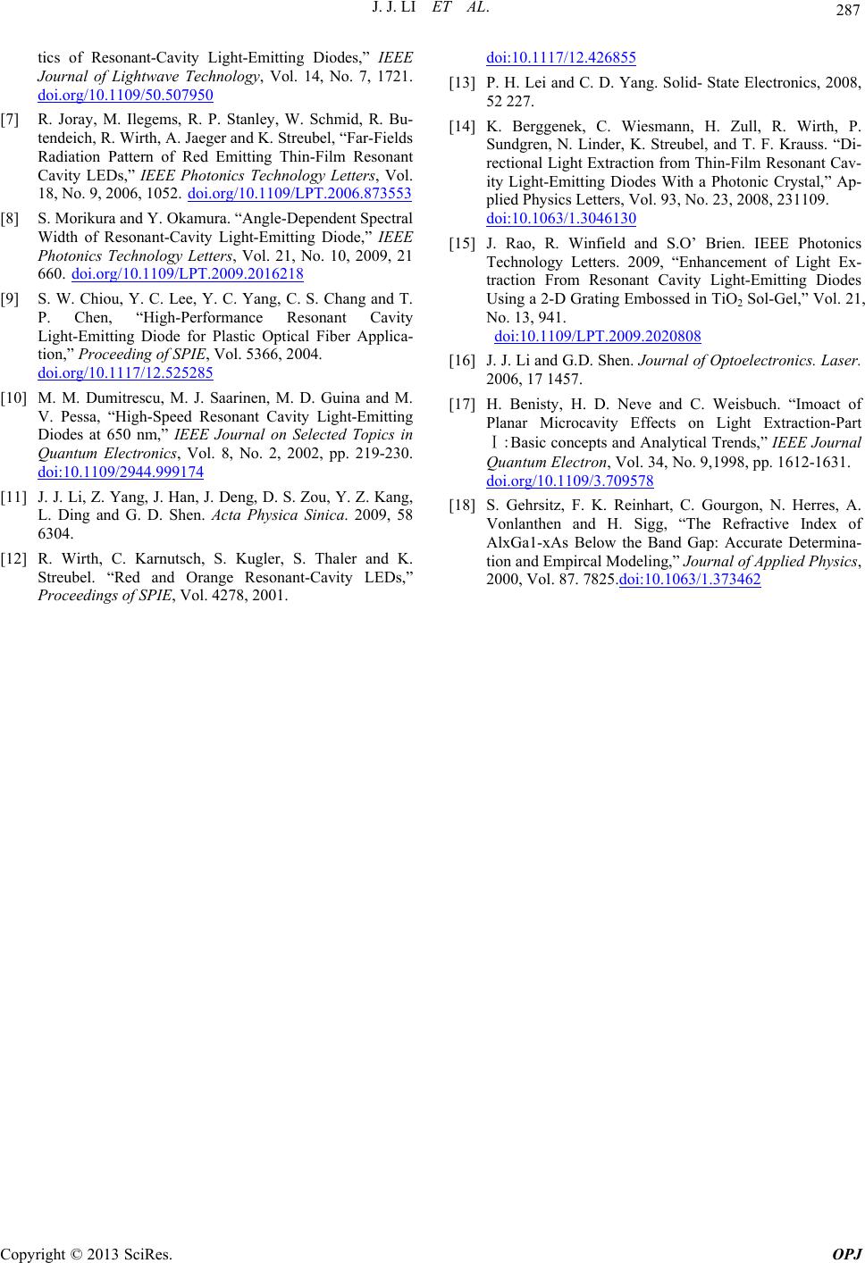 J. J. LI ET AL. Copyright © 2013 SciRes. OPJ 287 tics of Resonant-Cavity Light-Emitting Diodes,” IEEE Journal of Lightwave Technology, Vol. 14, No. 7, 1721. doi.org/10.1109/50.507950 [7] R. Joray, M. Ilegems, R. P. Stanley, W. Schmid, R. Bu- tendeich, R. Wirth, A. Jaeger and K. Streubel, “Far-Fields Radiation Pattern of Red Emitting Thin-Film Resonant Cavity LEDs,” IEEE Photonics Technology Letters, Vol. 18, No. 9, 2006, 1052. doi.org/10.1109/LPT.2006.873553 [8] S. Morikura and Y. Okamura. “Angle-Dependent Spectral Width of Resonant-Cavity Light-Emitting Diode,” IEEE Photonics Technology Letters, Vol. 21, No. 10, 2009, 21 660. doi.org/10.1109/LPT.2009.2016218 [9] S. W. Chiou, Y. C. Lee, Y. C. Yang, C. S. Chang and T. P. Chen, “High-Performance Resonant Cavity Light-Emitting Diode for Plastic Optical Fiber Applica- tion,” Proceeding of SPIE, Vol. 5366, 2004. doi.org/10.1117/12.525285 [10] M. M. Dumitrescu, M. J. Saarinen, M. D. Guina and M. V. Pessa, “High-Speed Resonant Cavity Light-Emitting Diodes at 650 nm,” IEEE Journal on Selected Topics in Quantum Electronics, Vol. 8, No. 2, 2002, pp. 219-230. doi:10.1109/2944.999174 [11] J. J. Li, Z. Yang, J. Han, J. Deng, D. S. Zou, Y. Z. Kang, L. Ding and G. D. Shen. Acta Physica Sinica. 2009, 58 6304. [12] R. Wirth, C. Karnutsch, S. Kugler, S. Thaler and K. Streubel. “Red and Orange Resonant-Cavity LEDs,” Proceedings of SPIE, Vol. 4278, 2001. doi:10.1117/12.426855 [13] P. H. Lei and C. D. Yang. Solid- State Electronics, 2008, 52 227. [14] K. Berggenek, C. Wiesmann, H. Zull, R. Wirth, P. Sundgren, N. Linder, K. Streubel, and T. F. Krauss. “Di- rectional Light Extraction from Thin-Film Resonant Cav- ity Light-Emitting Diodes With a Photonic Crystal,” Ap- plied Physics Letters, Vol. 93, No. 23, 2008, 231109. doi:10.1063/1.3046130 [15] J. Rao, R. Winfield and S.O’ Brien. IEEE Photonics Technology Letters. 2009, “Enhancement of Light Ex- traction From Resonant Cavity Light-Emitting Diodes Using a 2-D Grating Embossed in TiO2 Sol-Gel,” Vol. 21, No. 13, 941. doi:10.1109/LPT.2009.2020808 [16] J. J. Li and G.D. Shen. Journal of Optoelectronics. Laser. 2006, 17 1457. [17] H. Benisty, H. D. Neve and C. Weisbuch. “Imoact of Planar Microcavity Effects on Light Extraction-Part Ⅰ:Basic concepts and Analytical Trends,” IEEE Journal Quantum Electron, Vol. 34, No. 9,1998, pp. 1612-1631. doi.org/10.1109/3.709578 [18] S. Gehrsitz, F. K. Reinhart, C. Gourgon, N. Herres, A. Vonlanthen and H. Sigg, “The Refractive Index of AlxGa1-xAs Below the Band Gap: Accurate Determina- tion and Empircal Modeling,” Journal of Applied Physics, 2000, Vol. 87. 7825.doi:10.1063/1.373462 |