

Paper Menu >>
Journal Menu >>
 Optics and Photonics Journal, 2013, 3, 227-231 doi:10.4236/opj.2013.32B053 Published Online June 2013 (http://www.scirp.org/journal/opj) Maskless Microscopic Lithography through Shaping Ultraviolet Laser with Digital Micro-mirror Device Xiang-Yu Ding1, Yu-Xuan Ren2,3, Rong-De Lu1 1Department of Physics, University of Science and Technology of China, Hefei, China 2Institute of Biochemistry and Cell Biology, Shanghai Institutes for Biological Sciences, CAS, Shanghai, China 3National Center for Protein Sciences (Shanghai), Shanghai Institutes for Biological Sciences, CAS, Shanghai, China Email: [email protected], [email protected] Received 2013 ABSTRACT Laser shaping was introduced to maskless projection soft lithography by using digital micro-mirror device (DMD). The predesigned intensity pattern was imprinted onto the DMD and the input laser beam with a Gaussian or quasi-Gaussian distribution will carry the pattern on DMD to etch the resin. It provides a method of precise control of laser beam shapes and photon-induced curing behavior of resin. This technology provides an accurate micro-fabrication of micro- structures used for micro-systems. As a virtual mask generator and a binary-amplitude spatial light modulator, DMD is equivalent to the masks in the conventional exposure system. As the virtual masks and shaped laser beam can be achieved flexibly, it is a good method of precision soft lithography for 2D/3D microstructures. Keywords: Digital Micro-mirror Device (DMD); Laser Shaping; Maskless Projection; Soft Lithography 1. Introduction Micro-fabrication is essential to modern science and technology. As the most successful and main manufac- turing technology in micro-fabrication, lithography plays a great role since its invention in 1959 [1]. Although li- thography brings the rapid development of semiconduc- tor industry, there are rare applications in non-semicon- ductor areas, such as biology, chemistry, medicine, which require non-flat surfaces to fabricate on. Different from lithography, soft lithography is another micro-fabrication technology arose in 1990s [2], and it has wider applica- tions. It is a kind of micro-graphics replication technol- ogy. Just like a seal, it can copy micro-models to any surfaces without considering the flatness requirement. Physical masks and laser beam are two important ele- ments for both the conventional lithography and soft li- thography passing images to resin. Masks carry the images needed for carving. Laser beams transmit the images to resin. Although they work well together in the last dec- ades, physical masks require a long production cycle and can’ t be changed flexibly. Meanwhile the intensity of input laser beams used for resin exposure mainly has a Gaus- sian or quasi-Gaussian distribution which will causes the photon-induced curing behavior of resin with inverse Gaussian profile. In order to improve the performance, some new technology needed to be developed to over- come this obstacle. Digital micro-mirror device (DMD) is invented by Texas Instruments (TI)[3-5]. Since its introduction into market in 1996, it has become one of the most important devices in projection display field. DMD chips are adopted as the dynamic or virtual masks generator [6] with the help of aluminum micro-mirrors and it projects the vir- tual masks to resin or photo-resist. The lithography with DMD is maskless. Meanwhile, DMD can be treated as a kind of spatial light modulator in Digital Light Process- ing. It can be employed as a switch of light in a special direction and a laser shaper for laser beams. This paper introduces the laser shaping into maskless projection soft lithography by using DMD, error-diffu- sion algorithm and iterative refinement [7]. After laser shaping, the input laser beam with a Gaussian or quasi- Gaussian distribution will become a flat-top. By using the same method, many other laser intensity distributions can be achieved, such as tilted beam, dark hollow beam [8-10]. It provides a method of precise control of laser beam and photon-induced curing behavior of resin. Sec- tion 2 illustrates the experimental setup for soft lithogra- phy utilizing DMD. Section 3 introduces the experimen- tal process for resin coating and beam shaping. Section4 presents some of the preliminary experimental results and makes some discusses. 2. Experimental Setup The experimental setup is schematically shown in Figure 1. An LED (Thorlabs, LED365L2, F# 0.8, typical output Copyright © 2013 SciRes. OPJ  X. Y. DING ET AL. 228 power 360 mW) is employed as the laser source with dominant wavelength 365 nm. LED-illumination has the advantages of being low-cost, ease of use, and free of speckle-noise. The half divergence angle of the LED can be estimated from the F# to be 32°, therefore an anti- reflection coated aspheric condenser lens L1(ACL5040- A, Thorlabs) is introduced to collimate and expand the laser beam. The effective focal length of L1 is 40 mm and after expansion the diameter of the beam is approxi- mately 37 mm. The expanded beam illuminates the DMD with an incident angle of 24°. The DMD has a resolution of 1024 × 768 (Texas In- struments, width of mirror 13.68 μm). In order to control the DMD statuses, custom software written in Visual C++ 6.0 has been utilized to control the individual mi- cro-mirror. Lens L2 (f = 100 mm) collects the ultraviolet laser modulated by DMD and passes it through the pin- hole (tunable diameter) placed near the focus of Lens L2. The pinhole placed in here acts as a spatial filter for the purpose of enabling a good beam quality passing to the next section of the optical train. Lens L3 (f = 100 mm) and L4 (f = 100 mm) form a telescope system. The tele- scope relays the light field in the back focal plane (BFP) of lens L2 to the BFP of microscopic objective. The microscopic objective (LMU-10X-NUV, Thorlabs) utilized in our experimental setup is optimized for 325- 500 nm wavelength with a numerical aperture of 0.25. The magnification of the objective is 10X. The resin is placed on the focal plane of the microscopic objective. This plane is conjugated with the DMD surface. The etching optical path with DMD is employed as the pattern generator, and another counter propagating beam from a second LED with different wavelength is em- ployed to illuminate the sample stage and visualize the etched pattern. The wavelength of the second LED must have no influence on the resin in the irradiation process. A Dichroic mirror placed between Len L4 and the object- tive reflects the illumination light and a tube lens L5 im- ages the resin onto a USB CCD camera (DCU223M, 1024 × 768 pixels with pixel size of 4.65 × 4.65 μm2, Thorlabs Inc.,USA) which is also employed to capture the output profile of laser beam. The sample stage is a man- ual XY and Z-axis motorized translation stage (TSMW- XYZT-1, Zolix, China) that can be moved in 5 dimen- sions with minimum step of 100 μm and maximum angle of ±5o. Automated data collection, DMD patterns genera- tion, and motorized stage movement are implemented by custom software programmed in Visual C++ 6.0. 3. Experimental Procedure SU-8 (Microchem, 3050, negative photoresist) is chosen as the resin used in our experiment. High transmittance optical glass plates (50 × 60 mm) are employed as the sub-strate. Before resin preparation, it is necessary to clean the glass by acetone and methanol solution respec- tively. Wash the glass substrate with deionized water and dry the glass with nitrogen air. For safety, the whole process must be performed in the fume hood. The glass also needs to be heated on 200℃ through heating plate after cleaning to enhance the adhesion between the photoresist and the glass. As the substrate prepared already, it is time to handle the resin. The whole process of resin treatment includes resin coating, baking, exposure and development shown as in Figure 2. Firstly, the resin should be coated on the Figure 1. Experimental setup. The beam with dominate wavelength 365 nm is collimated and illuminated onto the DMD with incident angle of 24°. The predesigned pattern is loaded onto the DMD through a computer connected to the DMD electronic board. Lens L3 collects the imprinted la ser light and a consecuti ve pinhole enables the beam w ith a good quality through spatial filtering. A telescope formed by Lens L4 and L5 relay the BFP of L3 to BFP of the mi- croscopic objective. The glass slide with photosensitive re- sist if place onto a motorized translation stage. Custom software can be used to move the stage automatically through user- friendly software. A tube lens L5 images the chamber onto a CCD camera. Figure 2. (Color online) Resin preparation process. The whole preparation process of the resin is demonstrated on the left side. The picture on the right side shows typical experimental results or tools utilized in each step corresponding to the first column. The resin should be coated on the substrate by photoresist coating m achine with rotation speed of 2000 rpm for 30 s. The temperature and time recommended for resin baking is 65°for 6min and then 95°for 20 min. By utiliz- ing the shaped beam through DMD, the photo-resistive resin will be photo-cured. After development, the projected image will be imprinted on the resin. All the four processes should be performed in cleanroom without irradiance of UV light. Copyright © 2013 SciRes. OPJ 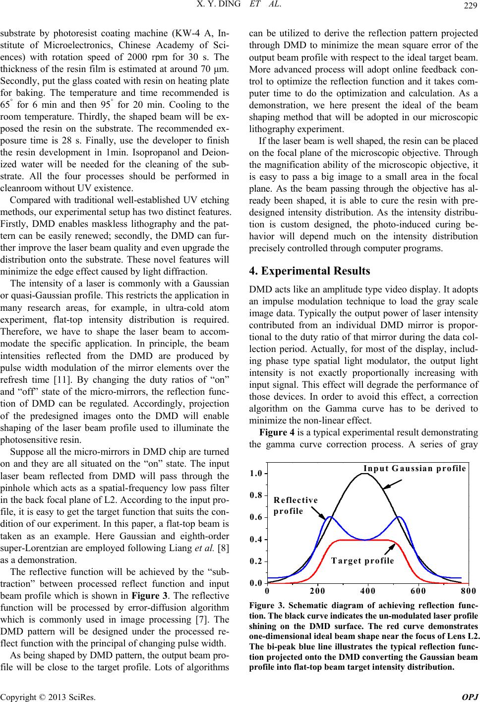 X. Y. DING ET AL. 229 substrate by photoresist coating machine (KW-4 A, In- stitute of Microelectronics, Chinese Academy of Sci- ences) with rotation speed of 2000 rpm for 30 s. The thickness of the resin film is estimated at around 70 μm. Secondly, put the glass coated with resin on heating plate for baking. The temperature and time recommended is 65° for 6 min and then 95° for 20 min. Cooling to the room temperature. Thirdly, the shaped beam will be ex- posed the resin on the substrate. The recommended ex- posure time is 28 s. Finally, use the developer to finish the resin development in 1min. Isopropanol and Deion- ized water will be needed for the cleaning of the sub- strate. All the four processes should be performed in cleanroom without UV existence. Compared with traditional well-established UV etching methods, our experimental setup has two distinct features. Firstly, DMD enables maskless lithography and the pat- tern can be easily renewed; secondly, the DMD can fur- ther improve the laser beam quality and even upgrade the distribution onto the substrate. These novel features will minimize the edge effect caused by light diffraction. The intensity of a laser is commonly with a Gaussian or quasi-Gaussian profile. This restricts the application in many research areas, for example, in ultra-cold atom experiment, flat-top intensity distribution is required. Therefore, we have to shape the laser beam to accom- modate the specific application. In principle, the beam intensities reflected from the DMD are produced by pulse width modulation of the mirror elements over the refresh time [11]. By changing the duty ratios of “on” and “off” state of the micro-mirrors, the reflection func- tion of DMD can be regulated. Accordingly, projection of the predesigned images onto the DMD will enable shaping of the laser beam profile used to illuminate the photosensitive resin. Suppose all the micro-mirrors in DMD chip are turned on and they are all situated on the “on” state. The input laser beam reflected from DMD will pass through the pinhole which acts as a spatial-frequency low pass filter in the back focal plane of L2. According to the input pro- file, it is easy to get the target function that suits the con- dition of our experiment. In this paper, a flat-top beam is taken as an example. Here Gaussian and eighth-order super-Lorentzian are employed following Liang et al. [8] as a demonstration. The reflective function will be achieved by the “sub- traction” between processed reflect function and input beam profile which is shown in Figure 3. The reflective function will be processed by error-diffusion algorithm which is commonly used in image processing [7]. The DMD pattern will be designed under the processed re- flect function with the principal of changing pulse width. As being shaped by DMD pattern, the output beam pro- file will be close to the target profile. Lots of algorithms can be utilized to derive the reflection pattern projected through DMD to minimize the mean square error of the output beam profile with respect to the ideal target beam. More advanced process will adopt online feedback con- trol to optimize the reflection function and it takes com- puter time to do the optimization and calculation. As a demonstration, we here present the ideal of the beam shaping method that will be adopted in our microscopic lithography experiment. If the laser beam is well shaped, the resin can be placed on the focal plane of the microscopic objective. Through the magnification ability of the microscopic objective, it is easy to pass a big image to a small area in the focal plane. As the beam passing through the objective has al- ready been shaped, it is able to cure the resin with pre- designed intensity distribution. As the intensity distribu- tion is custom designed, the photo-induced curing be- havior will depend much on the intensity distribution precisely controlled through computer programs. 4. Experimental Results DMD acts like an amplitude type video display. It adopts an impulse modulation technique to load the gray scale image data. Typically the output power of laser intensity contributed from an individual DMD mirror is propor- tional to the duty ratio of that mirror during the data col- lection period. Actually, for most of the display, includ- ing phase type spatial light modulator, the output light intensity is not exactly proportionally increasing with input signal. This effect will degrade the performance of those devices. In order to avoid this effect, a correction algorithm on the Gamma curve has to be derived to minimize the non-linear effect. Figure 4 is a typical experimental result demonstrating the gamma curve correction process. A series of gray 0 2 00 4 00 600 800 0.0 0.2 0.4 0.6 0.8 1.0 Inp u t G au ssian pr ofile Reflective p rofile T arget p rofile Figure 3. Schematic diagram of achieving reflection func- tion. The black curve indicates th e un-modulated laser profile shining on the DMD surface. The red curve demonstrates one-dimensional i deal beam shape near the focus of Lens L2. The bi-peak blue line illustrates the typical reflection func- tion projected onto the DMD converting the Gaussian beam profile into flat-top beam target intensit y di stribution. Copyright © 2013 SciRes. OPJ 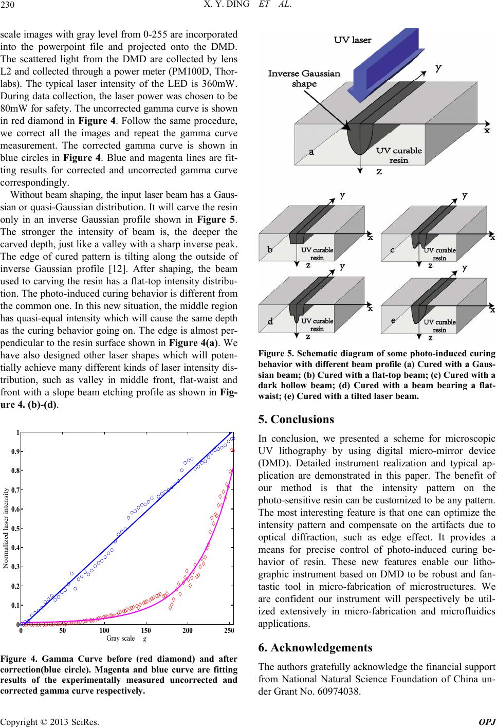 X. Y. DING ET AL. 230 scale images with gray level from 0-255 are incorporated into the powerpoint file and projected onto the DMD. The scattered light from the DMD are collected by lens L2 and collected through a power meter (PM100D, Thor- labs). The typical laser intensity of the LED is 360mW. During data collection, the laser power was chosen to be 80mW for safety. The uncorrected gamma curve is shown in red diamond in Figure 4. Follow the same procedure, we correct all the images and repeat the gamma curve measurement. The corrected gamma curve is shown in blue circles in Figure 4. Blue and magenta lines are fit- ting results for corrected and uncorrected gamma curve correspondingly. Without beam shaping, the input laser beam has a Gaus- sian or quasi-Gaussian distribution. It will carve the resin only in an inverse Gaussian profile shown in Figure 5. The stronger the intensity of beam is, the deeper the carved depth, just like a valley with a sharp inverse peak. The edge of cured pattern is tilting along the outside of inverse Gaussian profile [12]. After shaping, the beam used to carving the resin has a flat-top intensity distribu- tion. The photo-induced curing behavior is different from the common one. In this new situation, the middle region has quasi-equal intensity which will cause the same depth as the curing behavior going on. The edge is almost per- pendicular to the resin surface shown in Figure 4(a). We have also designed other laser shapes which will poten- tially achieve many different kinds of laser intensity dis- tribution, such as valley in middle front, flat-waist and front with a slope beam etching profile as shown in Fig- ure 4. (b)-(d). 050100 150 200 25 0 0 0.1 0.2 0.3 0.4 0.5 0.6 0.7 0.8 0.9 1 Gray scale g Normalized laser intensity Figure 4. Gamma Curve before (red diamond) and after correction(blue circle). Magenta and blue curve are fitting results of the experimentally measured uncorrected and corrected gamma curve respectively. Figure 5. Schemati c diagram of some photo-induced curing behavior with different beam profile (a) Cured with a Gaus- sian beam; (b) Cured with a flat-top beam; (c) Cured with a dark hollow beam; (d) Cured with a beam bearing a flat- waist; (e) Cured with a tilted laser beam. 5. Conclusions In conclusion, we presented a scheme for microscopic UV lithography by using digital micro-mirror device (DMD). Detailed instrument realization and typical ap- plication are demonstrated in this paper. The benefit of our method is that the intensity pattern on the photo-sensitive resin can be customized to be any pattern. The most interesting feature is that one can optimize the intensity pattern and compensate on the artifacts due to optical diffraction, such as edge effect. It provides a means for precise control of photo-induced curing be- havior of resin. These new features enable our litho- graphic instrument based on DMD to be robust and fan- tastic tool in micro-fabrication of microstructures. We are confident our instrument will perspectively be util- ized extensively in micro-fabrication and microfluidics applications. 6. Acknowledgements The authors gratefully acknowledge the financial support from National Natural Science Foundation of China un- der Grant No. 60974038. Copyright © 2013 SciRes. OPJ  X. Y. DING ET AL. Copyright © 2013 SciRes. OPJ 231 REFERENCES [1] Geppert, L., “Semiconductor Lithography for the Next Millennium,” IEEE Spectrum. Vol. 33, No. 4, 1996, p. 33-38. doi:10.1109/6.486632 [2] Y. Xia and G. M. Whitesides, “Soft Lithography,” Angewandte Chemie International Edition, Vol. 37, No. 5, 1998, pp. 550-575. doi:10.1002/(SICI)1521-3773(19980316)37:5<550::AID- ANIE550>3.0.CO;2-G [3] L. J. Hornbeck, “From Cathode Rays to Digital Micromirrors-A History of Electronic Projection Display Technology,” Texas Instruments Technical Journal, Vol. 15, No. 3,1998, pp. 7-46. [4] L. J. Hornbeck, “Current Status and Future Applications for DMD-Based Projection Displays,” Proceedings of the fifth International Display Workshop IDW '98, 1998, pp. 713-716. [5] P. F. Van Kessel,et al., “A MEMS-Based Projection Display,” Proceedings of the IEEE, 1998, Vol. 86, No.8, p. 1687-1704. doi:10.1109/5.704274 [6] A. Bertsch, J. Y. Jézéquel and J. C. André, “Study of the Spatial Resolution of A New 3D Microfabrication Process: The Microstereophotolithography Using A Dynamic Mask-Generator Technique,”Journal of Photochemistry and Photobiology A: Chemistry, 1997. Vol.107, No.1-3, pp. 275-281. doi:10.1016/S1010-6030(96)04585-6 [7] C. Dorrer and J. D. Zuegel, “Design and Analysis of Binary Beam Shapers Using Error Diffusion,”Journal of the Optical Society of America B-Optical Physics, Vol.24,No.6,2007,pp.1268-1275. doi:10.1364/JOSAB.24.001268 [8] J. Y. Liang, et al., “1.5% Root-Mean-Square Flat-Intensity Laser Beam Formed Using A Binary-Amplitude Spatial Light Modulator,”Applied Optics, Vol. 48, No.10, 2009, pp. 1955-1962. doi:10.1364/AO.48.001955 [9] J. Y. Liang, et al., “High-Precision Laser Beam Shaping Using A Binary-Amplitude Spatial Light Modulator,” Applied Optics, Vol.49,No.8, 2010, p. 1323-1330. doi:10.1364/AO.49.001323 [10] Y. X. Ren, et al., “Experimental Generation of Laguerre-Gaussian Beam Using Digital Micromirror Device,” Applied Optics, 2010, Vol. 49, No.10, pp. 1838-1844. doi:10.1364/AO.49.001838 [11] A. A. Adeyemi, N. Barakat and T.E. Darcie, “Applications of Digital Micro-Mirror Devices to Digital Optical Microscope Dynamic Range Enhancement,” Optics Express, Vol. 17, No.3, 2009, pp. 1831-1843. doi:10.1364/OE.17.001831 [12] C. Sun, et al., “Projection Micro-Stereolithography Using Digital Micro-Mirror Dynamic Mask,” Sensors and Actuators A: Physical, Vol. 121, No.1, 2005, pp. 113-120. doi:10.1016/j.sna.2004.12.011 [13] S. Zhao, H. Cong and T. Pan, “Direct Projection on Dry-Film Photoresist (DP2): Do-It-Yourself Three-Dimensional Polymer Microfluidics,” Lab on a Chip, Vol. 9, No. 8, 2009, pp. 1128-1132. doi:10.1039/b817925e [14] A. Waldbaur, et al., “Maskless Projection Lithography for the Fast and Flexible Generation of Grayscale Protein Patterns,” Small, Vol. 8, No.10, 2012,pp. 1570-1578. doi:10.1002/smll.201102163 |