

Paper Menu >>
Journal Menu >>
 Optics and Photonics Journal, 2013, 3, 209-211 doi:10.4236/opj.2013.32B049 Published Online June 2013 (http://www.scirp.org/journal/opj) Simulation and Design of a Low Crosstalk Hexagonal Photonic Crystal Crossover Waveguide Elnaz Pilehvar1, Hassan Kaatuzian1, Mohammad Danaie2 1Photonics Research Lab.(P.R.L.), Dept. of Electrical Engineering, Amirkabir University of Tech., Hafez Ave., Tehran, Iran 2Faculty of Elecrical Engineering, Semnan University, Semnan Email: [email protected] Received 2013 ABSTRACT In this paper, an optical waveguide junction is introduced to reduce crosstalk based on a hexagonal structure of photonic crystals for TE modes. The wavelength is 1330 nm which is an important wavelength for optical fiber data transmission. Simulation results show that the proposed design exhibits a reduction of -50 dB in crosstalk. It translates to a consider- able isolation improvement between two crossover waveguides. FDTD method is used to obtain the transmission coef- ficient. Keywords: Cross Talk; TE Mode; Waveguide; Hexagonal Photonic Crystal 1. Introduction Photonic crystals (PhC) are periodic optical structures that are designed to affect the light trajectory in dielectric or semiconductor waveguides[1].They have been devel- oped as building blocks for integrated photonic systems. In order to integrate multiple devices in a small region, it is necessary to have intersections of the waveguides which connect devices [2].The mentioned intersections should ideally have zero cross-talk. Photonic band gap (PBG) is essentially the gap be- tween the air-line and the dielectric-line in the dispersion relation of the PBG system [3]. In other word it is range of frequencies in which light is forbidden to propagate in crystal [4]. PhC behaves like a perfect mirror for light with frequency lying inside the band gap [5]. 2D-PhC’s, have two basic topologies. The first con- tains a dielectric substrate in which air holes are intro- duced periodically .The second one consists of dielectric rods embedded in air. Rod-type PhC has PBG for trans- verse magnetic (TM) modes and air-hole type has PBG for transverse electrical (TE) modes [6].Since the im- plementation of hole-type PhCs is easier, usually most structures realized in the literature have used it instead of the rod type alternative. A PhC waveguide can be constructed by removing one row of holes inside the otherwise perfect crystal [5]. For a two dimensional (2D) triangular lattice of air holes the hole radius of 0.45 a provides the largest band gap, al- though having a larger gap is a pre-requirement to achieving a wide-band single-mode waveguide but to avoid the structure becoming fragile, in most applications the radius of the most holes is not chosen larger than 0.3a [7]. In our design radii of some holes have been changed to achieve low crosstalk, high throughput for triangular lattice in TE mode in the important wavelength for opti- cal fiber data transmission that is 1.33 μ because of low dispersion [6].Various numerical methods can be used for analyzing PhC’s. Among this methods, finite-differ- ence time-domain (FDTD) is mostly used to obtain the throughput of the waveguide .It calculate the radiation field in open space by using appropriate boundry condi- tions [8].The numerical design of FDTD is described in section II. There is also a simulation and results section that explains the numerical simulation results. Finally we have a conclusion section. 2. Numerical Design The method we use to solve Maxwell’s equation in real space is called FDTD (Yee 1966). Figure 1 shows the Yee cell. It depicts the position of the electric and mag- netic field components [8]. Figure 1. Yee cell that shows the position of the electric and magnetic field components in 3D. Copyright © 2013 SciRes. OPJ 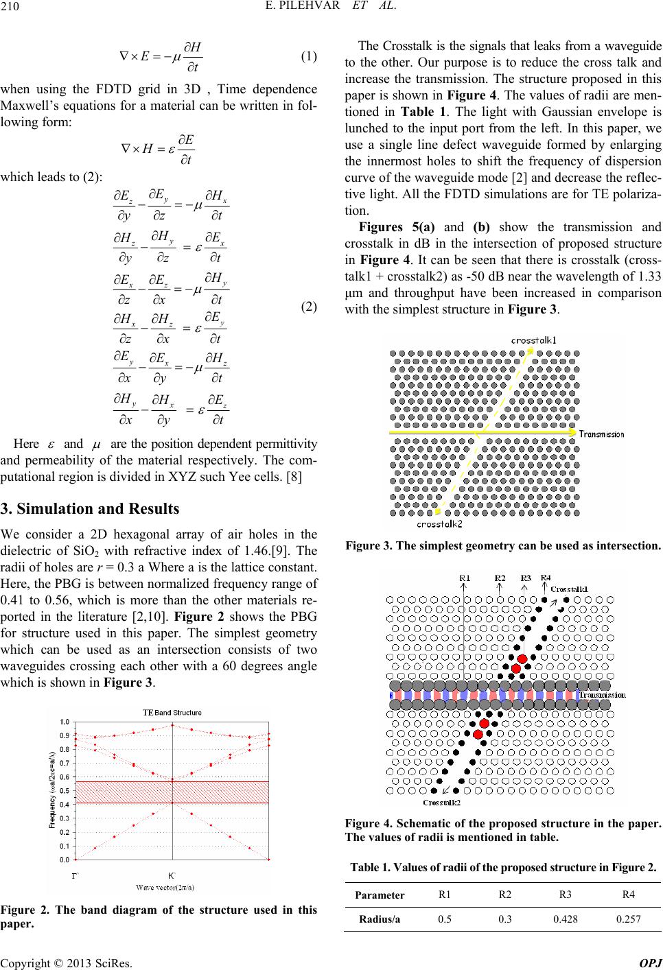 E. PILEHVAR ET AL. 210 H Et (1) when using the FDTD grid in 3D , Time dependence Maxwell’s equations for a material can be written in fol- lowing form: E Ht which leads to (2): y x z y x z y xz y xz yx z yx z E H E yz t HE H yz t H EE zx t E HH zx t EE H x yt HHE x yt (2) Here and are the position dependent permittivity and permeability of the material respectively. The com- putational region is divided in XYZ such Yee cells. [8] 3. Simulation and Results We consider a 2D hexagonal array of air holes in the dielectric of SiO2 with refractive index of 1.46.[9]. The radii of holes are r = 0.3 a Where a is the lattice constant. Here, the PBG is between normalized frequency range of 0.41 to 0.56, which is more than the other materials re- ported in the literature [2,10]. Figure 2 shows the PBG for structure used in this paper. The simplest geometry which can be used as an intersection consists of two waveguides crossing each other with a 60 degrees angle which is shown in Figure 3. Figure 2. The band diagram of the structure used in this paper. The Crosstalk is the signals that leaks from a waveguide to the other. Our purpose is to reduce the cross talk and increase the transmission. The structure proposed in this paper is shown in Figure 4. The values of radii are men- tioned in Table 1. The light with Gaussian envelope is lunched to the input port from the left. In this paper, we use a single line defect waveguide formed by enlarging the innermost holes to shift the frequency of dispersion curve of the waveguide mode [2] and decrease the reflec- tive light. All the FDTD simulations are for TE polariza- tion. Figures 5(a) and (b) show the transmission and crosstalk in dB in the intersection of proposed structure in Figure 4. It can be seen that there is crosstalk (cross- talk1 + crosstalk2) as -50 dB near the wavelength of 1.33 μm and throughput have been increased in comparison with the simplest structure in Figure 3. Figure 3. The simplest geometry can be used as intersection. Figure 4. Schematic of the proposed structure in the paper. The values of radii is mentioned in table. Table 1. Values of radii of the proposed stru cture in Figu re 2. Parameter R1 R2 R3 R4 Radius/a 0.5 0.3 0.428 0.257 Copyright © 2013 SciRes. OPJ 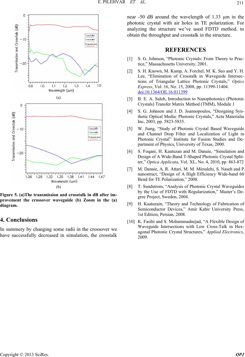 E. PILEHVAR ET AL. Copyright © 2013 SciRes. OPJ 211 (a) (b) Figure 5. (a)The transmission and crosstalk in dB after im- provement the crossover waveguide (b) Zoom in the (a) diagram. 4. Conclusions In summery by changing some radii in the crossover we have successfully decreased in simulation, the crosstalk near -50 dB around the wavelength of 1.33 μm in the photonic crystal with air holes in TE polarization. For analyzing the structure we’ve used FDTD method. to obtain the throughput and crosstalk in the structure. REFERENCES [1] S. G. Johnson, “Photonic Crystals: From Theory to Prac- tice,” Massachusetts University, 2001. [2] S. H. Known, M. Kamp, A. Forchel, M. K. Seo and Y. H. Lee, “Elimination of Crosstalk in Waveguide Intersec- tions of Triangular Lattice Photonic Crystals,” Optics Express, Vol. 16, No. 15, 2008, pp. 11399-11404. doi:10.1364/OE.16.011399 [3] B. E. A. Saleh, Introduction to Nanophotonics (Photonic Crystals) Transfer Matrix Method (TMM), Module 1 [4] S. G. Johnson and J. D. Joannopoulos, “Designing Syn- thetic Optical Media: Photonic Crystals,” Acta Materialia Inc, 2003, pp. 5823-5835. [5] W. Jiang, “Study of Photonic Crystal Based Waveguide and Channel Drop Filter and Localization of Light in Photonic Crystal” Institute for Fusion Studies and De- partment of Physics, University of Texas, 2000. [6] S. Foqani, H. Kaatuzan and M. Danaie, “Simulation and Design of A Wide-Band T-Shaped Photonic Crystal Split- ter,” Optica A pplicata, Vol. XL, No. 4, 2010, pp. 863-872 [7] M. Danaie, A. R. Attari, M. M. Mirsalehi, S. Naseh and P. nanostruct, “Design of A High Efficiency Wide-band 60 Bend for TE Polarization,” 2008. [8] T. Sundstrom, “Analysis of Photonic Crystal Waveguides by the Use of FDTD with Regularization,” Master’s De- gree Project, Sweden, 2004. [9] H. Kaatuzain, “Theory and Technology of Fabrication of Semiconductor Devices,” Amir Kabir University Press, 1st Edition, Persian, 2008. [10] K. Fasihi and S. Mohammadnejad, “A Flexible Design of Waveguide Intersections with Low Cross-Talk in Hex- agonal Photonic Crystal Structures,” Applied Electronics, 2009. |