

Paper Menu >>
Journal Menu >>
 Optics and Photonics Journal, 2013, 3, 158-161 doi:10.4236/opj.2013.32B038 Published Online June 2013 (http://www.scirp.org/journal/opj) Design of Thermo-Optic Variable Optical Attenu ator Based on Quartz Substrate Hongqing Dai1, Junming An1,2, Liangliang Wang1, Yue Wang1, Liyao Zhang1, Jiashun Zhang1,2, Hongjie Wang1,2, Pan Pan1, Xiaogu ang Z hang1, Ruidan Liu1, Jianguang Li1,2,Yuanda Wu1,2, Xiongwei Hu1 1Institute of Semiconductors, Chinese Academy of Sciences, Beijing, China 2Henan Shijia Photons Technology Co., Ltd, Hebi, China Email: [email protected] Received 2013 ABSTRACT In this paper, we designed a thermo-optic variable optical attenuator (VOA) based on quartz substrate, which consists of a Mach-Zehnder interferometer (MZI) and a thin film heater above the phase-modulation arm. The transmission proper- ties of the waveguide and attenuation characteristics of the device have been simulated by beam propagation method (BPM), and the simulated results illustrated that the designed VOA had good performance. Keywords: VOA; MZI; Thermo-optic; Quartz Substrate 1. Introduction Variable optical attenuator (VOA) is one of the most basic optical passive devices in modern optical network, with a wide range of applications in optical communica- tion and its main function is to control and attenuate op- tical signal power. With the application of dense wave- length division multiplexing (DWDM) system, to realiz- ing optical signal propagation in high speed correctly, we need to monitor and balance the multi-channel optical power, resulting in dynamic channel equalizer (DCE), variable optical attenuator integrated multiplexer/demul- tiplexer (VMUX), optical add-drop multiplexer and other optical devices. VOA is the core component of these devices and plays a very important role in the gain con- trol of linear-repeaters for wavelength division multi- plexed networks and channel power equalization in wavelength division multiplexing (WDM) cross-connect nodes. The study of PLC-VOA has just started in our country, but the demand for VOAs is larger and larger with the progress of optical communication. Only the new optical attenuators of low cost, easy integration, and good performance can meet the growing market demand [1,2]. SiO2 material has a lot of advantages compared with other materials that are used in the manufacture of optical waveguide devices from early times. The coupling loss of optical waveguide devices produced between SiO2 planar waveguide and single-mode fiber is quite low. The transmission loss of the optical signal in SiO2 material is only 0.2dB/km. The SiO2 material has certain thermo- optic coefficient and thus can be used for the modulation of refractive index. The devices based on SiO2 materials can be directly grown on Si or quartz substrate, which can be integrated with other Si based waveguide devices. The SiO2 material also has great environment stability. Internationally, most of the VOAs have been fabricated were based on the Si substrate and there was an under- cladding layer between the core and the substrate. In this paper, we designed a Mach-Zehnder interferometer (MZI) thermo-optic variable optical attenuator based on quartz substrate. It eliminated the step of the fabrication of the underclading layer, simplifying the manufacture process. The core and the substrate could match better because they were composed of the same material of SiO2. Re- sults of the simulation of the waveguide transmission properties and device attenuation properties illustrated that the designed VOA had good performance. 2. The Principles of VOAs The structure of the MZI thermo-optic VOA based on quartz substrate is shown in Figure 1. It consists of in- put/output waveguide, two Y-branches, two symmetrical phase-modulation arms, and a metal film heater above one of the arms. The input light signal is split to two identical light signals in the first Y-branch region. Then the two beams of light will pass through the two arms separately and interfere in the second Y-branch region. If the two arms are completely symmetrical, the output Copyright © 2013 SciRes. OPJ 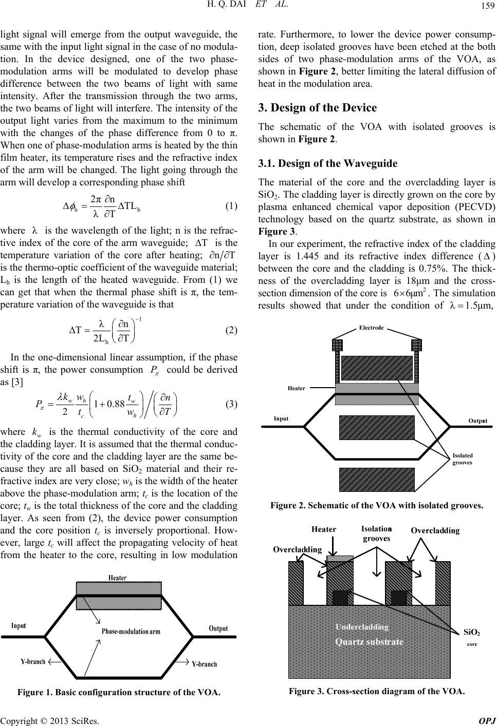 H. Q. DAI ET AL. 159 light signal will emerge from the output waveguide, the same with the input light signal in the case of no modula- tion. In the device designed, one of the two phase- modulation arms will be modulated to develop phase difference between the two beams of light with same intensity. After the transmission through the two arms, the two beams of light will interfere. The intensity of the output light varies from the maximum to the minimum with the changes of the phase difference from 0 to π. When one of phase-modulation arms is heated by the thin film heater, its temperature rises and the refractive index of the arm will be changed. The light going through the arm will develop a corresponding phase shift h 2πTL λT n h (1) where is the wavelength of the light; n is the refrac- tive index of the core of the arm waveguide; λ T is the temperature variation of the core after heating; nT is the thermo-optic coefficient of the waveguide material; Lh is the length of the heated waveguide. From (1) we can get that when the thermal phase shift is π, the tem- perature variation of the waveguide is that 1 h λn T2L T (2) In the one-dimensional linear assumption, if the phase shift is π, the power consumption P could be derived as [3] 10.88 2 wh w h c kw tn PwT t (3) where w is the thermal conductivity of the core and the cladding layer. It is assumed that the thermal conduc- tivity of the core and the cladding layer are the same be- cause they are all based on SiO2 material and their re- fractive index are very close; wh is the width of the heater above the phase-modulation arm; tc is the location of the core; tw is the total thickness of the core and the cladding layer. As seen from (2), the device power consumption and the core position tc is inversely proportional. How- ever, large tc will affect the propagating velocity of heat from the heater to the core, resulting in low modulation k Figure 1. Basic configuration structure of the VOA. rate. Furthermore, to lower the device power consump- tion, deep isolated grooves have been etched at the both sides of two phase-modulation arms of the VOA, as shown in Figure 2, better limiting the lateral diffusion of heat in the modulation area. 3. Design of the Device The schematic of the VOA with isolated grooves is shown in Figure 2. 3.1. Design of the Waveguide The material of the core and the overcladding layer is SiO2. The cladding layer is directly grown on the core by plasma enhanced chemical vapor deposition (PECVD) technology based on the quartz substrate, as shown in Figure 3. In our experiment, the refractive index of the cladding layer is 1.445 and its refractive index difference ( ) between the core and the cladding is 0.75%. The thick- ness of the overcladding layer is 18μm and the cross- section dimension of the core is . The simulation results showed that under the condition of 2 66μm λ1.5μm, Figure 2. Schematic of the VOA with isolated grooves. Figure 3. Cross-section diagram of the VOA. Copyright © 2013 SciRes. OPJ 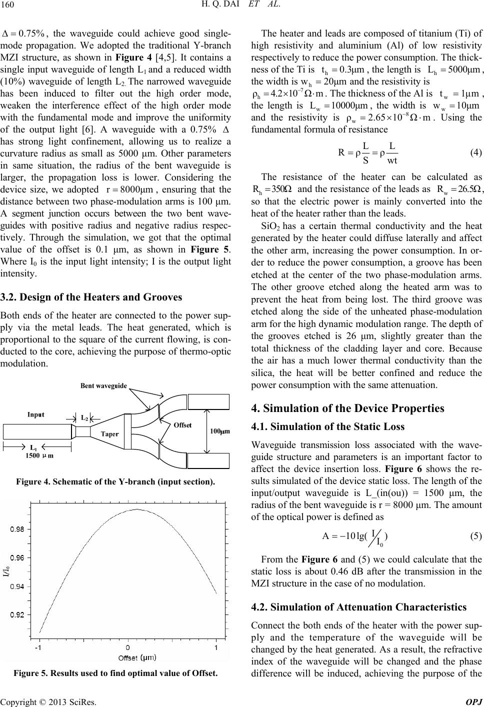 H. Q. DAI ET AL. 160 0.75% , the waveguide could achieve good single- mode propagation. We adopted the traditional Y-branch MZI structure, as shown in Figure 4 [4,5]. It contains a single input waveguide of length L1 and a reduced width (10%) waveguide of length L2. The narrowed waveguide has been induced to filter out the high order mode, weaken the interference effect of the high order mode with the fundamental mode and improve the uniformity of the output light [6]. A waveguide with a 0.75% has strong light confinement, allowing us to realize a curvature radius as small as 5000 μm. Other parameters in same situation, the radius of the bent waveguide is larger, the propagation loss is lower. Considering the device size, we adopted , ensuring that the distance between two phase-modulation arms is 100 μm. A segment junction occurs between the two bent wave- guides with positive radius and negative radius respec- tively. Through the simulation, we got that the optimal value of the offset is 0.1 μm, as shown in Figure 5. Where I0 is the input light intensity; I is the output light intensity. r80 m 00μ 3.2. Design of the Heaters and Grooves Both ends of the heater are connected to the power sup- ply via the metal leads. The heat generated, which is proportional to the square of the current flowing, is con- ducted to the core, achieving the purpose of thermo-optic modulation. Figure 4. Schematic of the Y-branc h (input section). Figure 5. Results used to find optimal value of Offset. The heater and leads are composed of titanium (Ti) of high resistivity and aluminium (Al) of low resistivity respectively to reduce the power consumption. The thick- ness of the Ti is h t0.3μm , the length is h L 5000μm , the width is h w20μm and the resistivity is 7Ω h ρ4.2 10m . The thickness of the Al is w t1μm , is w L10000μm the length , the width is w w10μm stivity is w ρ2.65 10 and the resi8Ω m fundamental formula of resistance . Using the LL Rρρ Sw t (4) The resistance of the heater can be calculated as h R350Ω and the resistance of the leads as w R26.5Ω , so that the electric power is mainly converted into the heat of the heater rather than the leads. SiO2 has a certain thermal conductivity and the heat generated by the heater could diffuse laterally and affect the other arm, increasing the power consumption. In or- der to reduce the power consumption, a groove has been etched at the center of the two phase-modulation arms. The other groove etched along the heated arm was to prevent the heat from being lost. The third groove was etched along the side of the unheated phase-modulation arm for the high dynamic modulation range. The depth of the grooves etched is 26 μm, slightly greater than the total thickness of the cladding layer and core. Because the air has a much lower thermal conductivity than the silica, the heat will be better confined and reduce the power consumption with the same attenuation. 4. Simulation of the Device Properties 4.1. Simulation of the Static Loss Waveguide transmission loss associated with the wave- guide structure and parameters is an important factor to affect the device insertion loss. Figure 6 shows the re- sults simulated of the device static loss. The length of the input/output waveguide is L_(in(ou)) = 1500 μm, the radius of the bent waveguide is r = 8000 μm. The amount of the optical power is defined as 0 I A10lg( I ) (5) From the Figure 6 and (5) we could calculate that the static loss is about 0.46 dB after the transmission in the MZI structure in the case of no modulation. 4.2. Simulation of Attenuation Characteristics Connect the both ends of the heater with the power sup- ply and the temperature of the waveguide will be changed by the heat generated. As a result, the refractive index of the waveguide will be changed and the phase difference will be induced, achieving the purpose of the Copyright © 2013 SciRes. OPJ 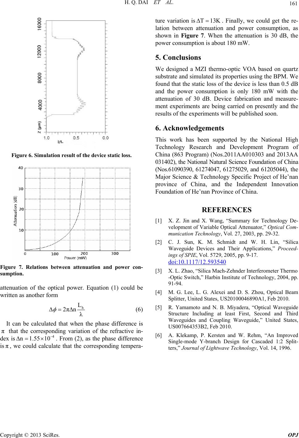 H. Q. DAI ET AL. Copyright © 2013 SciRes. OPJ 161 Figure 6. Simulation result of the device static loss. Figure 7. Relations between attenuation and power con- sumption. attenuation of the optical power. Equation (1) could be written as another form h L 2πnλ (6) It can be calculated that when the phase difference is that the corresponding variation of the refractive in- dex is. From (2), as the phase difference is , we could calculate that the corresponding tempera- ture variation is π π 4 n1.5510 T13K . Finally, we could get the re- lation between attenuation and power consumption, as shown in Figure 7. When the attenuation is 30 dB, the power consumption is about 180 mW. 5. Conclusions We designed a MZI thermo-optic VOA based on quartz substrate and simulated its properties using the BPM. We found that the static loss of the device is less than 0.5 dB and the power consumption is only 180 mW with the attenuation of 30 dB. Device fabrication and measure- ment experiments are being carried on presently and the results of the experiments will be published soon. 6. Acknowledgements This work has been supported by the National High Technology Research and Development Program of China (863 Program) (Nos.2011AA010303 and 2013AA 031402), the National Natural Science Foundation of China (Nos.61090390, 61274047, 61275029, and 61205044), the Major Science & Technology Specific Project of He’nan province of China, and the Independent Innovation Foundation of He’nan Province of China. REFERENCES [1] X. Z. Jin and X. Wang, “Summary for Technology De- velopment of Variable Optical Attenuator,” Optical Com- munication Technology, Vol. 27, 2003, pp. 29-32. [2] C. J. Sun, K. M. Schmidt and W. H. Lin, “Silica Waveguide Devices and Their Applications,” Proceed- ings of SPIE, Vol. 5729, 2005, pp. 9-17. doi:10.1117 /12.593540 [3] X. L. Zhao, “Silica Mach-Zehnder Interferometer Thermo -Optic Switch,” Harbin Institute of Technology, 2004, pp. 91-94. [4] M. G. Lee, L. G. Alexei and D. S. Zhou, Optical Beam Splitter, United States, US20100046890A1, Feb 2010. [5] R. Yamamoto and N. B. Miyadera, “Optical Waveguide Structure Including at least First, Second and Third Waveguides and Coupling Waveguide,” United States, US007664353B2, Feb 2010. [6] A. Klekamp, P. Kersten and W. Rehm, “An Improved Single-mode Y-branch Design for Cascaded 1:2 Split- ters,” Journal of Lightwave Technology, Vol. 14, 1996. |