

Paper Menu >>
Journal Menu >>
 Journal of Modern Physics, 2013, 4, 994-999 http://dx.doi.org/10.4236/jmp.2013.47134 Published Online July 2013 (http://www.scirp.org/journal/jmp) Superinjection from Oriented Carbyne as the Result of Landau Quantization in Giant Pseudo-Magnetic Field Yuri Prazdnikov Faculty of Physics, Moscow State University, Moscow, Russia Email: [email protected] Received April 25, 2013; revised May 26, 2013; accepted June 25, 2013 Copyright © 2013 Yuri Prazdnikov. This is an open access article distributed under the Creative Commons Attribution License, which permits unrestricted use, distribution, and reproduction in any medium, provided the original work is properly cited. ABSTRACT The qualitative explanation of the earlier published experimental data was obtained within new energetic model of ori- ented carbyne. The conductivity spectrum and the superinjection effect feature Landau quantization in a giant pseudo- magnetic field. The relativistic dispersion of carriers and non-dissipative character of their motion cause the effect of superinjection where carriers go upwards on an energetic ladder. Raman-spectra and other data point out to the fact that the plane of carriers’ motion is close to the carbyne-insulator interface. Quantum effects and on-surface conductivity allow considering oriented carbyne as an analogue of topological insulator. Keywords: Carbyne; Superinjection; Pseudo-Magnetic Field; Topological Insulator 1. Introduction The arguments in favor of idea that the carbon era only begins are given in [1]. Although sp1 carbon—carbyne was discovered by Russian chemist A. M. Sladkov al- ready more than half a century ago [2], it is still men- tioned as a perspective material by Russian scientists only. This characterizes well the majority of world scien- tists’ respect to carbyne in general and its oriented form in particular. Carbyne chains with the length of 44 atoms were synthesized recently by authors [3] and this realized as a small sensation. They see big future for carbyne’s application in the molecular electronics. At the same time, Russian publications about carbyne chains of hundreds atoms length still remain unnoted. These articles present experimental results that clearly favor the unique struc- ture and properties of oriented carbyne. The main effects are resistance quantization at room temperature [4] and abnormal injection/emission capability [5,6]. Ideal re- peatability of current-voltage characteristics (CVC), quantization at room temperature and integration possi- bility into the existing technology nowadays allow us to consider oriented carbyne as one of the most promising materials for nanoelectronics [7]. So what is the reason of such sustainable skepticism by world's scientists? One of the main reasons for skepticism is the lack of an accu- rate theoretical model. This is due to the complexity of modeling such nanosystems. The theory of topological insulator [8,9] and the pseudo quantum Hall Effect in two-dimensional systems have been developed not so far [10]. Another skeptic’s important argument is that insta- bility of pure carbon sp1 chains does not concern the ori- ented form of carbyne. Individual carbon sp1 chains are really not stable; they should be packed into the oriented quasicrystal to be able to exist as a chain of hundreds atoms. But even in this form carbyne can’t be obtained in a large size crystal. This fact still has no correct explana- tion and this is another skeptical argument. Has long been noticed the key role of the surface where oriented carbyne is growing up (at the thickness of more than 1 micron oriented carbyne turns into an amor- phous mixture of different phases of carbon). It has re- cently become clear that the stability can be related to presence of molecular hydrogen in interchain space [11]. The Author proposed new model of interchain dihydro- gen bonds based on data about mass-spectra of the laser ablation products. Electrical conductivity of oriented carbyne is anisot- ropic: chains are minimal quantum wires with ballistic electron transport regime in longitudinal direction. There- fore an electric field (unlike a magnetic one) inside car- byne is two-dimensional. Conductivity across chains has roughly an exponentially-stepped dependence on the thickness of a carbyne film [4]. The spectrum of “magic” thicknesses where the conductivity increases abruptly had been discovered by authors, but its origin was not clear. C opyright © 2013 SciRes. JMP 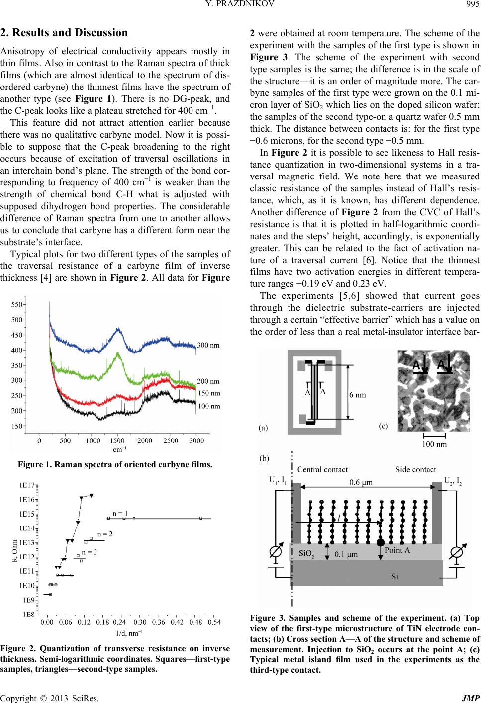 Y. PRAZDNIKOV 995 2. Results and Discussion Anisotropy of electrical conductivity appears mostly in thin films. Also in contrast to the Raman spectra of thick films (which are almost identical to the spectrum of dis- ordered carbyne) the thinnest films have the spectrum of another type (see Figure 1). There is no DG-peak, and the C-peak looks like a plateau stretched for 400 cm−1. This feature did not attract attention earlier because there was no qualitative carbyne model. Now it is possi- ble to suppose that the C-peak broadening to the right occurs because of excitation of traversal oscillations in an interchain bond’s plane. The strength of the bond cor- responding to frequency of 400 cm−1 is weaker than the strength of chemical bond С-Н what is adjusted with supposed dihydrogen bond properties. The considerable difference of Raman spectra from one to another allows us to conclude that carbyne has a different form near the substrate’s interface. Typical plots for two different types of the samples of the traversal resistance of a carbyne film of inverse thickness [4] are shown in Figure 2. All data for Figure Figure 1. Raman spectra of oriented carbyne films. Figure 2. Quantization of transverse resistance on inverse thickness. Semi-logarithmic coordinates. Squares—first-type samples, triangles—second-type samples. 2 were obtained at room temperature. The scheme of the experiment with the samples of the first type is shown in Figure 3. The scheme of the experiment with second type samples is the same; the difference is in the scale of the structure—it is an order of magnitude more. The car- byne samples of the first type were grown on the 0.1 mi- cron layer of SiO2 which lies on the doped silicon wafer; the samples of the second type-on a quartz wafer 0.5 mm thick. The distance between contacts is: for the first type −0.6 microns, for the second type −0.5 mm. In Figure 2 it is possible to see likeness to Hall resis- tance quantization in two-dimensional systems in a tra- versal magnetic field. We note here that we measured classic resistance of the samples instead of Hall’s resis- tance, which, as it is known, has different dependence. Another difference of Figure 2 from the CVC of Hall’s resistance is that it is plotted in half-logarithmic coordi- nates and the steps’ height, accordingly, is exponentially greater. This can be related to the fact of activation na- ture of a traversal current [6]. Notice that the thinnest films have two activation energies in different tempera- ture ranges −0.19 eV and 0.23 eV. The experiments [5,6] showed that current goes through the dielectric substrate-carriers are injected through a certain “effective barrier” which has a value on the order of less than a real metal-insulator interface bar- Figure 3. Samples and scheme of the experiment. (a) Top view of the first-type microstructure of TiN electrode con- tacts; (b) Cross section A—A of the structure and scheme of measurement. Injection to SiO2 occurs at the point A; (c) Typical metal island film used in the experiments as the third-type contact. Copyright © 2013 SciRes. JMP 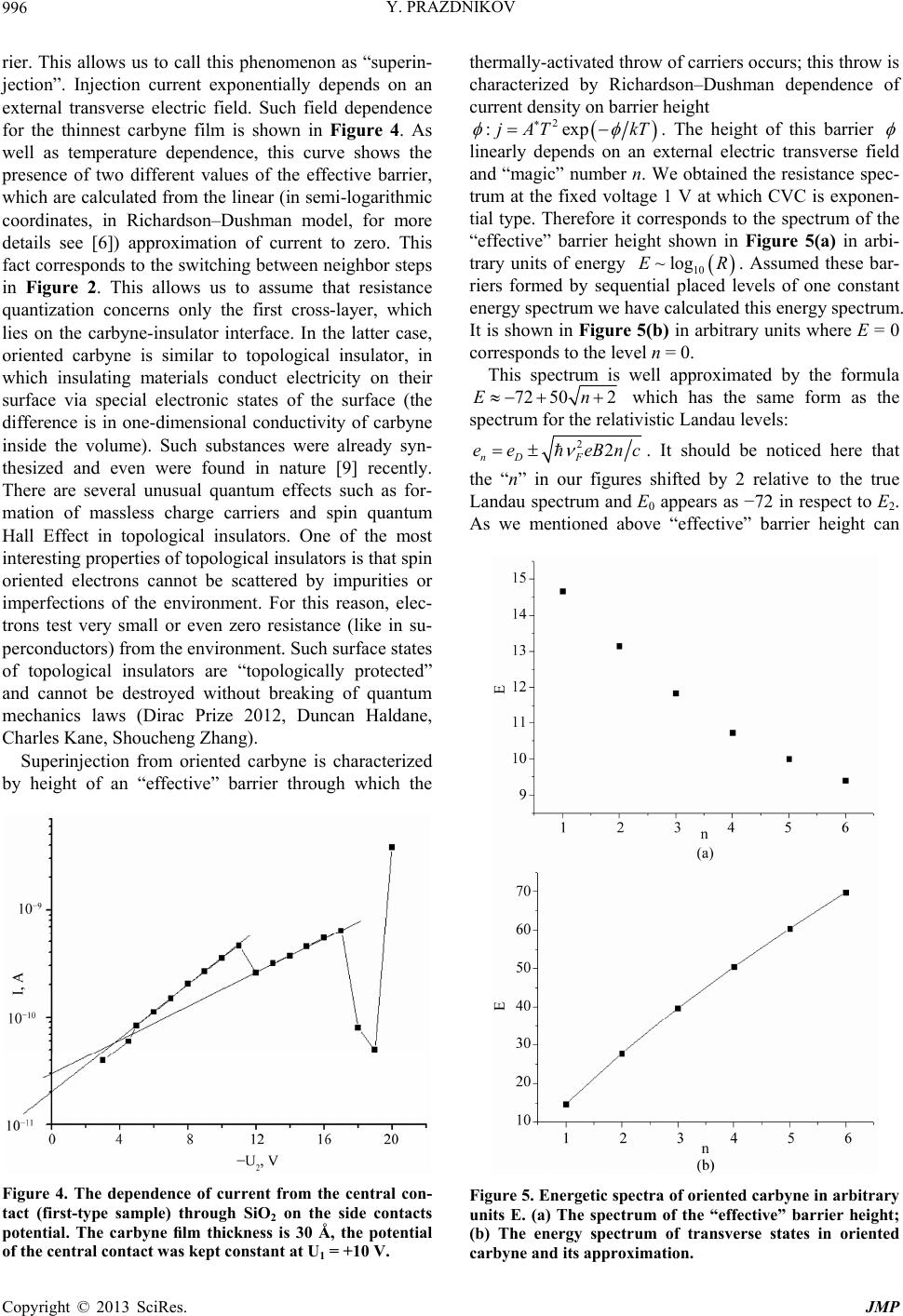 Y. PRAZDNIKOV 996 rier. This allows us to call this phenomenon as “superin- jection”. Injection current exponentially depends on an external transverse electric field. Such field dependence for the thinnest carbyne film is shown in Figure 4. As well as temperature dependence, this curve shows the presence of two different values of the effective barrier, which are calculated from the linear (in semi-logarithmic coordinates, in Richardson–Dushman model, for more details see [6]) approximation of current to zero. This fact corresponds to the switching between neighbor steps in Figure 2. This allows us to assume that resistance quantization concerns only the first cross-layer, which lies on the carbyne-insulator interface. In the latter case, oriented carbyne is similar to topological insulator, in which insulating materials conduct electricity on their surface via special electronic states of the surface (the difference is in one-dimensional conductivity of carbyne inside the volume). Such substances were already syn- thesized and even were found in nature [9] recently. There are several unusual quantum effects such as for- mation of massless charge carriers and spin quantum Hall Effect in topological insulators. One of the most interesting properties of topological insulators is that spin oriented electrons cannot be scattered by impurities or imperfections of the environment. For this reason, elec- trons test very small or even zero resistance (like in su- perconductors) from the environment. Such surface states of topological insulators are “topologically protected” and cannot be destroyed without breaking of quantum mechanics laws (Dirac Prize 2012, Duncan Haldane, Charles Kane, Shoucheng Zhang). Superinjection from oriented carbyne is characterized by height of an “effective” barrier through which the Figure 4. The dependence of current from the central con- tact (first-type sample) through SiO2 on the side contacts potential. The carbyne film thickness is 30 Å, the potential of the central contact was kept constant at U1 = +10 V. thermally-activated throw of carriers occurs; this throw is characterized by Richardson–Dushman dependence of current density on barrier height 2 :expjAT kT . The height of this barrier linearly depends on an external electric transverse field and “magic” number n. We obtained the resistance spec- trum at the fixed voltage 1 V at which CVC is exponen- tial type. Therefore it corresponds to the spectrum of the “effective” barrier height shown in Figure 5(a) in arbi- trary units of energy 10 . Assumed these bar- riers formed by sequential placed levels of one constant energy spectrum we have calculated this energy spectrum. It is shown in Figure 5(b) in arbitrary units where E = 0 corresponds to the level n = 0. ~logER This spectrum is well approximated by the formula 72 502En which has the same form as the spectrum for the relativistic Landau levels: 22 nD F ee eBnc . It should be noticed here that the “n” in our figures shifted by 2 relative to the true Landau spectrum and E0 appears as −72 in respect to E2. As we mentioned above “effective” barrier height can Figure 5. Energetic spectra of oriented carbyne in arbitrary units E. (a) The spectrum of the “effective” barrier height; (b) The energy spectrum of transverse states in oriented carbyne and its approximation. Copyright © 2013 SciRes. JMP  Y. PRAZDNIKOV 997 easily be switched by transversal electric field or tem- perature or film thickness. Thus we could not find an absolute value and used the relative “n”. Each level of the Landau spectrum corresponds to the cyclotron orbit of massless charge carriers—Dirac fermions. Theoreti- cally their presence is possible in 2D dihydrogen trans- verse chain layer. As we noted above, at least one such layer exists at the carbyne-insulator interface, and this can cause Dirac fermions appearance by analogy to to- pological insulators. The question about the origin of a quantizing magnetic field oriented along the chains arises. A possibility of formation so-called “pseudo-magnetic” field in graphene by its deformation is discussed in [10]. Its value is so large that it is able to cause Landau quantization at room temperature. In the article [12] experimental evidence of existence of such a field in graphene is obtained, and its value is estimated to be hundreds of Tesla, what allow authors to call it “giant pseudo-magnetic”. It is interest- ing to note that oriented carbyne on pictures taken by an atomic-force microscope has the unit cell a bit extended in a traversal plane; this strain can induce a pseudo- magnetic field. The presence of a magnetic field can explain the pre- viously noticed strong dependence of the injection/emis- sion current on the environment. First of all, it is the in- fluence of the substrate. In Figure 2 the difference in spectra for samples on a thin dielectric layer and the solid dielectric is visible. The quantization of the “magic” thicknesses on n and its approximation by a cubic parab- ola is presented in Figure 6 for two types of the samples. As it could be seen from the approximations, the magic thicknesses grow ≈40 times faster by n in the samples of the first type than in the second: 3 23 2.5n 3 .6 1.9n 73d for samples of the first type, and 59 0d for the second ones. Secondly, it is the influence of the interelectrode vac- uum space width on the current of emission of electrons into vacuum. This fact previously had no clear explana- tion [6]. It is difficult to explain such strong influence by a space charge field: the electron cloud density is con- centrated near emission center (i.e., near the carbyne surface). Figure 7 shows the set of CVC’s of current of electron emission into vacuum from the samples of the third type where oriented carbyne was grown on Cu is- land film (50 nm) laying on a dielectric layer. These samples have the same carbyne-in-wells type and are characterized by the same CVC’s of injection/emission current as the samples of the first two types, but the cur- rent area is greater. Let’s note here the independence of super—injection/emission on geometry and defects—an island metal film which is used as a well-type contact in the third type samples is characterized by the size and Figure 6. The spectra of “magic” thicknesses and their ap- proximations by cubic parabola. (a) First-type samples: d = 73 + 23 × (n − 2.5)3; (b) Second-type samples: d = 59 + 0.6 × (n + 1.9)3. Figure 7. Electron emission from third-type samples. The value of the interelectrode vacuum space is: (1) d = 0.4 mm; (2) d = 0.08 mm; (3) d = 0.04 mm. Copyright © 2013 SciRes. JMP 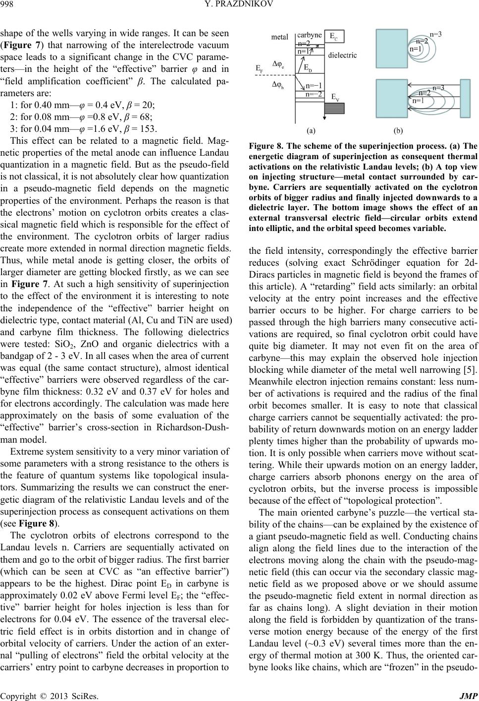 Y. PRAZDNIKOV 998 shape of the wells varying in wide ranges. It can be seen (Figure 7) that narrowing of the interelectrode vacuum space leads to a significant change in the CVC parame- ters—in the height of the “effective” barrier φ and in “field amplification coefficient” β. The calculated pa- rameters are: 1: for 0.40 mm—φ = 0.4 eV, β = 20; 2: for 0.08 mm—φ =0.8 eV, β = 68; 3: for 0.04 mm—φ =1.6 eV, β = 153. This effect can be related to a magnetic field. Mag- netic properties of the metal anode can influence Landau quantization in a magnetic field. But as the pseudo-field is not classical, it is not absolutely clear how quantization in a pseudo-magnetic field depends on the magnetic properties of the environment. Perhaps the reason is that the electrons’ motion on cyclotron orbits creates a clas- sical magnetic field which is responsible for the effect of the environment. The cyclotron orbits of larger radius create more extended in normal direction magnetic fields. Thus, while metal anode is getting closer, the orbits of larger diameter are getting blocked firstly, as we can see in Figure 7. At such a high sensitivity of superinjection to the effect of the environment it is interesting to note the independence of the “effective” barrier height on dielectric type, contact material (Al, Cu and TiN are used) and carbyne film thickness. The following dielectrics were tested: SiO2, ZnO and organic dielectrics with a bandgap of 2 - 3 eV. In all cases when the area of current was equal (the same contact structure), almost identical “effective” barriers were observed regardless of the car- byne film thickness: 0.32 eV and 0.37 eV for holes and for electrons accordingly. The calculation was made here approximately on the basis of some evaluation of the “effective” barrier’s cross-section in Richardson-Dush- man model. Extreme system sensitivity to a very minor variation of some parameters with a strong resistance to the others is the feature of quantum systems like topological insula- tors. Summarizing the results we can construct the ener- getic diagram of the relativistic Landau levels and of the superinjection process as consequent activations on them (see Figure 8). The cyclotron orbits of electrons correspond to the Landau levels n. Carriers are sequentially activated on them and go to the orbit of bigger radius. The first barrier (which can be seen at CVC as “an effective barrier”) appears to be the highest. Dirac point ED in carbyne is approximately 0.02 eV above Fermi level EF; the “effec- tive” barrier height for holes injection is less than for electrons for 0.04 eV. The essence of the traversal elec- tric field effect is in orbits distortion and in change of orbital velocity of carriers. Under the action of an exter- nal “pulling of electrons” field the orbital velocity at the carriers’ entry point to carbyne decreases in proportion to Figure 8. The scheme of the superinjection process. (a) The energetic diagram of superinjection as consequent thermal activations on the relativistic Landau levels; (b) A top view on injecting structure—metal contact surrounded by car- byne. Carriers are sequentially activated on the cyclotron orbits of bigger radius and finally injected downwards to a dielectric layer. The bottom image shows the effect of an external transversal electric field—circular orbits extend into elliptic, and the orbital speed becomes variable. the field intensity, correspondingly the effective barrier reduces (solving exact Schrödinger equation for 2d- Diracs particles in magnetic field is beyond the frames of this article). A “retarding” field acts similarly: an orbital velocity at the entry point increases and the effective barrier occurs to be higher. For charge carriers to be passed through the high barriers many consecutive acti- vations are required, so final cyclotron orbit could have quite big diameter. It may not even fit on the area of carbyne—this may explain the observed hole injection blocking while diameter of the metal well narrowing [5]. Meanwhile electron injection remains constant: less num- ber of activations is required and the radius of the final orbit becomes smaller. It is easy to note that classical charge carriers cannot be sequentially activated: the pro- bability of return downwards motion on an energy ladder plenty times higher than the probability of upwards mo- tion. It is only possible when carriers move without scat- tering. While their upwards motion on an energy ladder, charge carriers absorb phonons energy on the area of cyclotron orbits, but the inverse process is impossible because of the effect of “topological protection”. The main oriented carbyne’s puzzle—the vertical sta- bility of the chains—can be explained by the existence of a giant pseudo-magnetic field as well. Conducting chains align along the field lines due to the interaction of the electrons moving along the chain with the pseudo-mag- netic field (this can occur via the secondary classic mag- netic field as we proposed above or we should assume the pseudo-magnetic field extent in normal direction as far as chains long). A slight deviation in their motion along the field is forbidden by quantization of the trans- verse motion energy because of the energy of the first Landau level (~0.3 eV) several times more than the en- ergy of thermal motion at 300 K. Thus, the oriented car- byne looks like chains, which are “frozen” in the pseudo- Copyright © 2013 SciRes. JMP 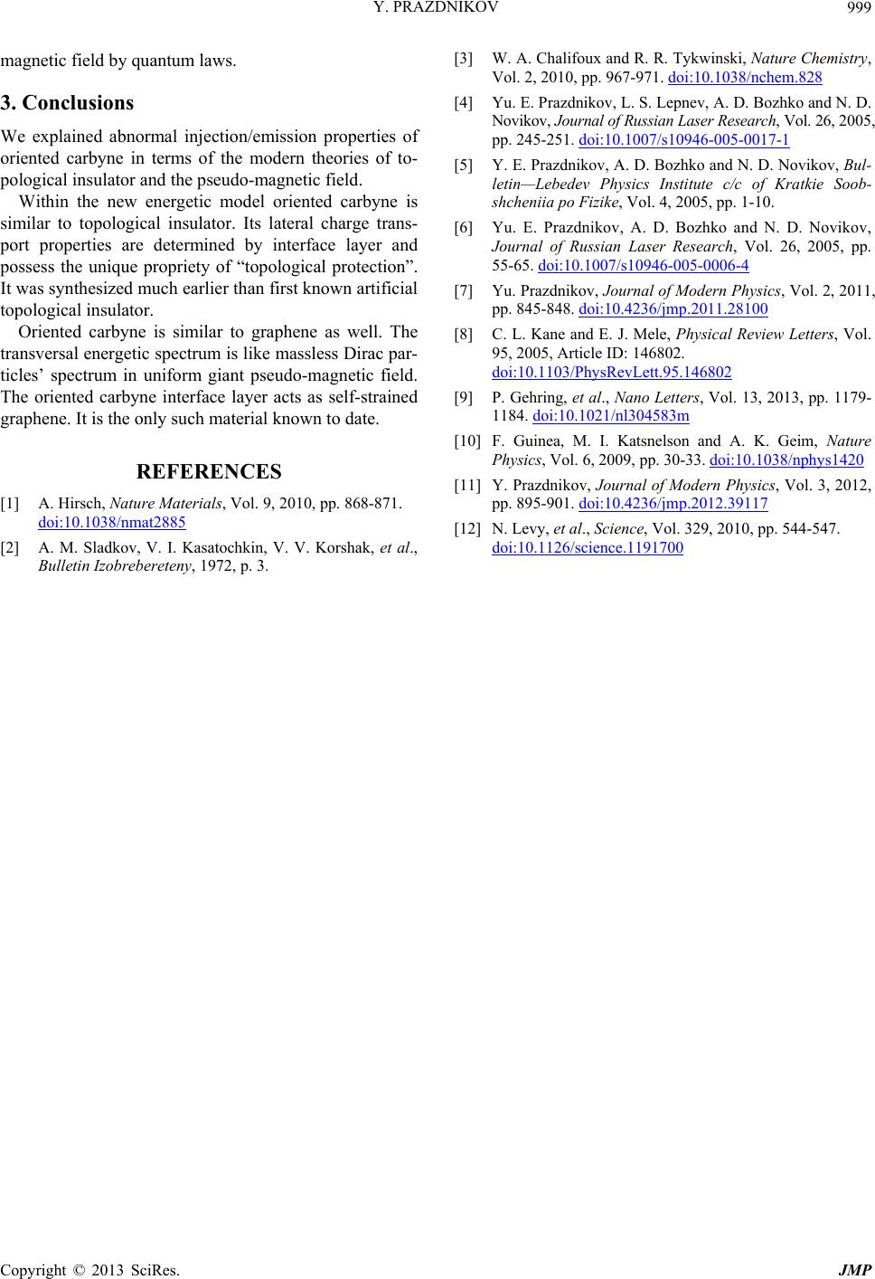 Y. PRAZDNIKOV Copyright © 2013 SciRes. JMP 999 magnetic field by quantum laws. 3. Conclusions We explained abnormal injection/emission properties of oriented carbyne in terms of the modern theories of to- pological insulator and the pseudo-magnetic field. Within the new energetic model oriented carbyne is similar to topological insulator. Its lateral charge trans- port properties are determined by interface layer and possess the unique propriety of “topological protection”. It was synthesized much earlier than first known artificial topological insulator. Oriented carbyne is similar to graphene as well. The transversal energetic spectrum is like massless Dirac par- ticles’ spectrum in uniform giant pseudo-magnetic field. The oriented carbyne interface layer acts as self-strained graphene. It is the only such material known to date. REFERENCES [1] A. Hirsch, Nature Materials, Vol. 9, 2010, pp. 868-871. doi:10.1038/nmat2885 [2] A. M. Sladkov, V. I. Kasatochkin, V. V. Korshak, et al., Bulletin Izobrebereteny, 1972, p. 3. [3] W. A. Chalifoux and R. R. Tykwinski, Nature Chemistry, Vol. 2, 2010, pp. 967-971. doi:10.1038/nchem.828 [4] Yu. E. Prazdnikov, L. S. Lepnev, A. D. Bozhko and N. D. Novikov, Journal of Russian Laser Research, Vol. 26, 2005, pp. 245-251. doi:10.1007/s10946-005-0017-1 [5] Y. E. Prazdnikov, A. D. Bozhko and N. D. Novikov, Bul- letin—Lebedev Physics Institute c/c of Kratkie Soob- shcheniia po Fizike, Vol. 4, 2005, pp. 1-10. [6] Yu. E. Prazdnikov, A. D. Bozhko and N. D. Novikov, Journal of Russian Laser Research, Vol. 26, 2005, pp. 55-65. doi:10.1007/s10946-005-0006-4 [7] Yu. Prazdnikov, Journal of Modern Physics, Vol. 2, 2011, pp. 845-848. doi:10.4236/jmp.2011.28100 [8] C. L. Kane and E. J. Mele, Physical Review Letters, Vol. 95, 2005, Article ID: 146802. doi:10.1103/PhysRevLett.95.146802 [9] P. Gehring, et al., Nano Letters, Vol. 13, 2013, pp. 1179- 1184. doi:10.1021/nl304583m [10] F. Guinea, M. I. Katsnelson and A. K. Geim, Nature Physics, Vol. 6, 2009, pp. 30-33. doi:10.1038/nphys1420 [11] Y. Prazdnikov, Journal of Modern Physics, Vol. 3, 2012, pp. 895-901. doi:10.4236/jmp.2012.39117 [12] N. Levy, et al., Science, Vol. 329, 2010, pp. 544-547. doi:10.1126/science.1191700 |