

Paper Menu >>
Journal Menu >>
 Circuits and Systems, 2013, 4, 323-327 http://dx.doi.org/10.4236/cs.2013.43044 Published Online July 2013 (http://www.scirp.org/journal/cs) A CMOS 3.1 - 10.6 GHz UWB LNA Employing Modified Derivative Superposition Method Amir Homaee Staff in Iranian Offshore Oil Company (IOOC), Tehran, Iran Email: [email protected] Received October 19, 2012; revised January 7, 2013; accepted January 15, 2013 Copyright © 2013 Amir Homaee. This is an open access article distributed under the Creative Commons Attribution License, which permits unrestricted use, distribution, and reproduction in any medium, provided the original work is properly cited. ABSTRACT Low noise amplifier (LNA) performs as the initial amplification block in the receive path in a radio frequency (RF) re- ceiver. In this work an ultra-wideband 3.1 - 10.6-GHz LNA is discussed. By using the proposed circuits for RF CMOS LNA and design methodology, the noise from the device is decreased across the ultra wide band (UWB) band. The measured noise figure is 2.66 - 3 dB over 3.1 - 10.6-GHz, while the power gain is 14 ± 0.8 dB. It consumes 23.7 mW from a 1.8 V supply. The input and output return losses (S11 & S22) are less than –11 dB over the UWB band. By using the modified derivative superposition method, the third-order intercept point IIP3 is improved noticeably. The complete circuit is based on the 0.18 μm standard RFCMOS technology and simulated with Hspice simulator. Keywords: Broadband; Low-Noise Amplifier (LNA); Noise Figure; Ultra-Wideband (UWB); Modified Derivative Superposition Method 1. Introduction Development of the high-speed wireless communication systems puts increasing request on integrated low-cost RF devices with multi-GHz bandwidth operating at the lowest power consumption and supply voltage. Ultra wide band (IEEE 802.15.3a) appears as a new technol- ogy capable for high data transfer rates (up to 1 Gb/s) within short distances (10 m) at low power. This tech- nology uses for some application such as wireless per- sonal area networks (WPANs), providing an environment for transmission of audio, video, and other high-band- width data [1]. The amplifier that is used for this applica- tion must meet several requirements. For example to in- terface with the preselect filter and antenna, the amplifier input impedance should be close to 50 over the desired UWB band. However sufficient gain with wide band width to overtop the noise of a mixer, low noise figure to improve receiver sensitivity, low power consumption to increase battery life, small die area to reduce the cost, unconditional stability and good linearity are important parameters. There is a close trade-off between them. There are some proposed solutions and circuits for each parameter [2-8]. However, some parameters would be ruined by improving the others [4]. In this research a new circuit has achieved via modifying these methods [1,9]. The main parameter in this research is noise figure which has noticeably improved in comparison with the other references. It is 2.66 - 3 dB over 3.1 - 10.6-GHz band width. 2. Input Stage Common-gate and Cascode configurations are two kinds of methods usually used to design the input stage of LNA in CMOS circuits, while the Common-Gate and Cascode structure provides a wide-band and narrow-band input matching respectively. However Common-gate stage has an intrinsically high noise figure versus Cascode stage and the noise-canceling techniques must be used. In the narrow band application, a shunt inductor is added in the input stage to resonate with Cgs to enhance impedance matching at the desired frequency. However in most CMOS narrow band applications, cascode LNA with inductive degeneration is preferable but for isolating from the input to the output and omitting of the Cgd path, the Common-Gate LNA performs better reverse isolation and stability versus Common-Source LNA. Numerical value for the lower bound is about 2.2 dB for long-channel devices and 4.8 dB for short channel devices. 3. Circuit Design and Analysis The proposed wide-band LNA is shown in Figure 1. C opyright © 2013 SciRes. CS 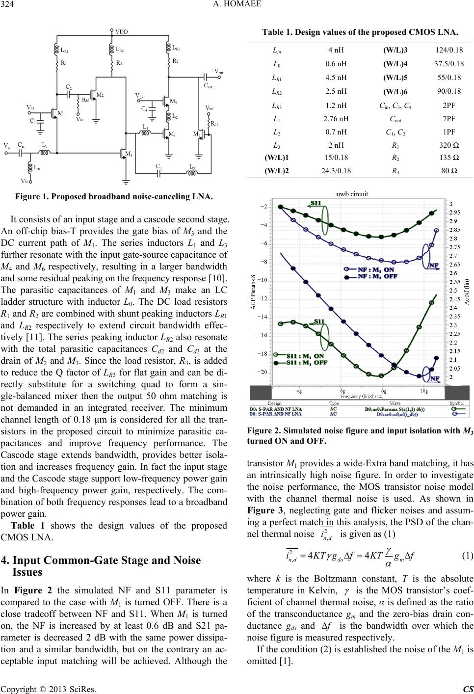 A. HOMAEE 324 Figure 1. Proposed broadband noise-canceling LNA. It consists of an input stage and a cascode second stage. An off-chip bias-T provides the gate bias of M3 and the DC current path of M1. The series inductors L1 and L3 further resonate with the input gate-source capacitance of M4 and M6 respectively, resulting in a larger bandwidth and some residual peaking on the frequency response [10]. The parasitic capacitances of M1 and M3 make an LC ladder structure with inductor L0. The DC load resistors R1 and R2 are combined with shunt peaking inductors LR1 and LR2 respectively to extend circuit bandwidth effec- tively [11]. The series peaking inductor LR2 also resonate with the total parasitic capacitances Cd2 and Cd3 at the drain of M2 and M3. Since the load resistor, R3, is added to reduce the Q factor of LR3 for flat gain and can be di- rectly substitute for a switching quad to form a sin- gle-balanced mixer then the output 50 ohm matching is not demanded in an integrated receiver. The minimum channel length of 0.18 μm is considered for all the tran- sistors in the proposed circuit to minimize parasitic ca- pacitances and improve frequency performance. The Cascode stage extends bandwidth, provides better isola- tion and increases frequency gain. In fact the input stage and the Cascode stage support low-frequency power gain and high-frequency power gain, respectively. The com- bination of both frequency responses lead to a broadband power gain. Table 1 shows the design values of the proposed CMOS LNA. 4. Input Common-Gate Stage and Noise Issues In Figure 2 the simulated NF and S11 parameter is compared to the case with M1 is turned OFF. There is a close tradeoff between NF and S11. When M1 is turned on, the NF is increased by at least 0.6 dB and S21 pa- rameter is decreased 2 dB with the same power dissipa- tion and a similar bandwidth, but on the contrary an ac- ceptable input matching will be achieved. Although the Table 1. Design values of the proposed CMOS LNA. Lin 4 nH (W/L)3 124/0.18 L0 0.6 nH (W/L)4 37.5/0.18 LR1 4.5 nH (W/L)5 55/0.18 LR2 2.5 nH (W/L)6 90/0.18 LR3 1.2 nH Cin, C3, C4 2PF L1 2.76 nH Cout 7PF L2 0.7 nH C1, C2 1PF L3 2 nH R1 320 Ω (W/L)1 15/0.18 R2 135 Ω (W/L)2 24.3/0.18 R3 80 Ω Figure 2. Simulated noise figure and input isolation with M3 turned ON and OFF. transistor M1 provides a wide-Extra band matching, it has an intrinsically high noise figure. In order to investigate the noise performance, the MOS transistor noise model with the channel thermal noise is used. As shown in Figure 3, neglecting gate and flicker noises and assum- ing a perfect match in this analysis, the PSD of the chan- nel thermal noise 2 ,nd i is given as (1) 2 ,44 nd dom iKTgfKTgf (1) where k is the Boltzmann constant, T is the absolute temperature in Kelvin, is the MOS transistor’s coef- ficient of channel thermal noise, α is defined as the ratio of the transconductance gm and the zero-bias drain con- ductance gds and f is the bandwidth over which the noise figure is measured respectively. If the condition (2) is established the noise of the M1 is omitted [1]. Copyright © 2013 SciRes. CS 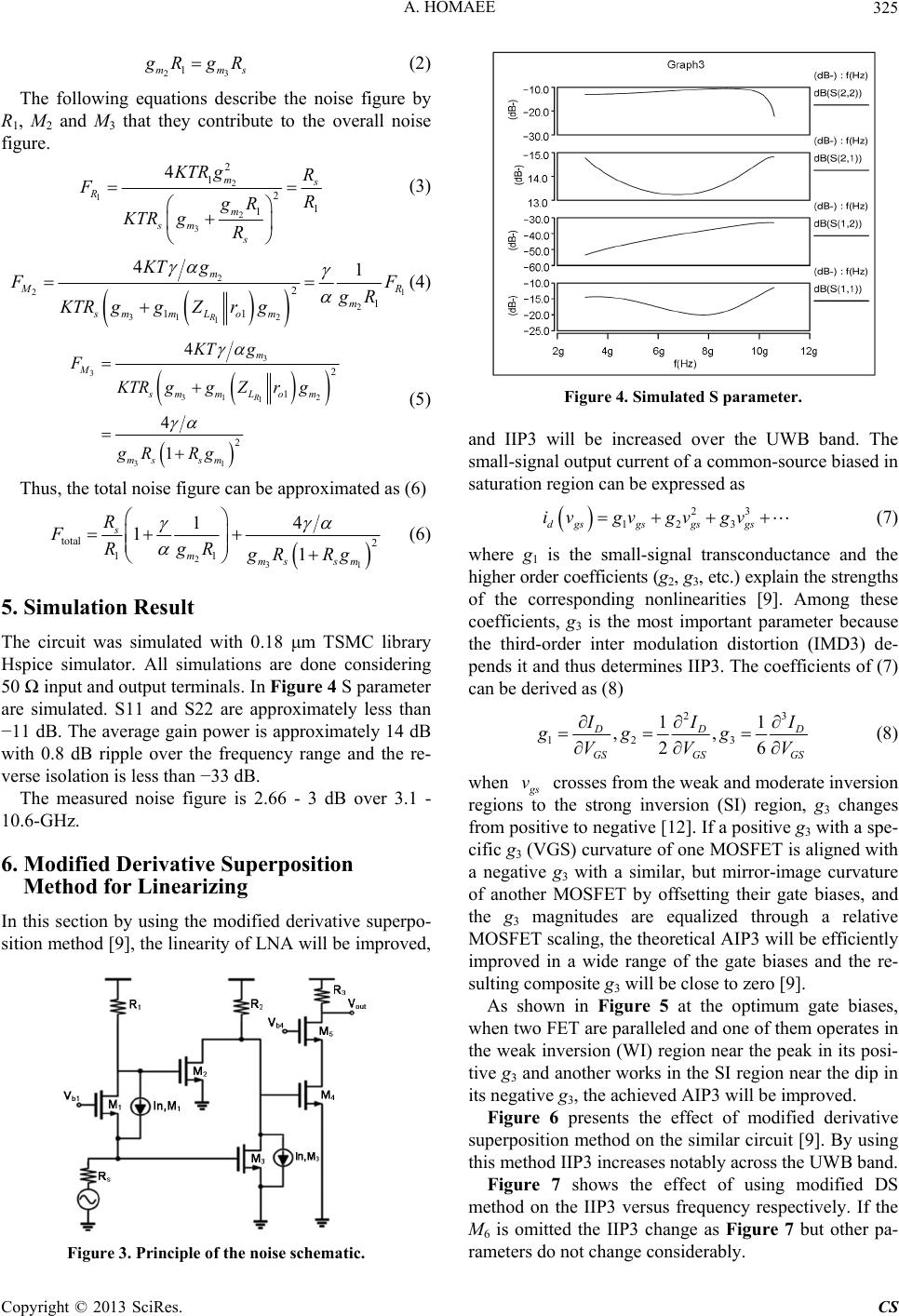 A. HOMAEE 325 g 23 1mms RgR (2) The following equations describe the noise figure by R1, M2 and M 3 that they contribute to the overall noise figure. 2 2 2 2 1 1 m 1 3 1 4 s R sm KTR g F KTR g m s R R gR R (3) 2 2 31 2 1 2 11 4 R m 1 21 1 M R m smmL om KT g F F gR KTR ggZrg (4) 3 2 1 2 1 3 31 31 2 4 4 1 M sm m ms sm KT F KTR ggZ gR Rg R m L om g r g (5) Thus, the total noise figure can be approximated as (6) 2 total 11 1 s mms R FRgR gR 31 2 14 1sm Rg (6) 5. Simulation Result The circuit was simulated with 0.18 μm TSMC library Hspice simulator. All simulations are done considering 50 Ω input and output terminals. In Figure 4 S parameter are simulated. S11 and S22 are approximately less than −11 dB. The average gain power is approximately 14 dB with 0.8 dB ripple over the frequency range and the re- verse isolation is less than −33 dB. The measured noise figure is 2.66 - 3 dB over 3.1 - 10.6-GHz. 6. Modified Derivative Superposition Method for Linearizing In this section by using the modified derivative superpo- sition method [9], the linearity of LNA will be improved, Figure 3. Principle of the noise schematic. Figure 4. Simulated S paramete r . and IIP3 will be increased over the UWB band. The small-signal output current of a common-source biased in saturation region can be expressed as 23 123dgsgs gs gs ivgvgv gv (7) where g1 is the small-signal transconductance and the higher order coefficients (g2, g3, etc.) explain the strengths of the corresponding nonlinearities [9]. Among these coefficients, g3 is the most important parameter because the third-order inter modulation distortion (IMD3) de- pends it and thus determines IIP3. The coefficients of (7) can be derived as (8) 23 12 3 11 ,, 26 D DD GSGS GS I II gg g VVV (8) when g s crosses from the weak and moderate inversion regions to the strong inversion (SI) region, g3 changes from positive to negative [12]. If a positive g3 with a spe- cific g3 (VGS) curvature of one MOSFET is aligned with a negative g3 with a similar, but mirror-image curvature of another MOSFET by offsetting their gate biases, and the g3 magnitudes are equalized through a relative MOSFET scaling, the theoretical AIP3 will be efficiently improved in a wide range of the gate biases and the re- sulting composite g3 will be close to zero [9]. As sho v wn in Figure 5 at the optimum gate biases, w tive su m hen two FET are paralleled and one of them operates in the weak inversion (WI) region near the peak in its posi- tive g3 and another works in the SI region near the dip in its negative g3, the achieved AIP3 will be improved. Figure 6 presents the effect of modified deriva perposition method on the similar circuit [9]. By using this method IIP3 increases notably across the UWB band. Figure 7 shows the effect of using modified DS ethod on the IIP3 versus frequency respectively. If the M6 is omitted the IIP3 change as Figure 7 but other pa- rameters do not change considerably. Copyright © 2013 SciRes. CS 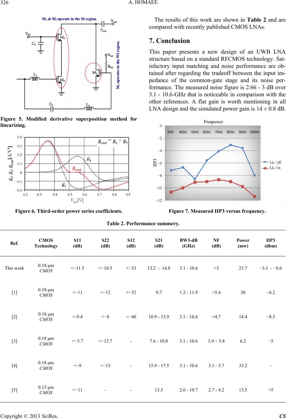 A. HOMAEE Copyright © 2013 SciRes. CS 326 The results of this work are shown in Table 2 and are compared with recently published CMOS LNAs. 7. Conclusion This paper presents a new design of an UWB LNA structure based on a standard RFCMOS technology. Sat- isfactory input matching and noise performance are ob- tained after regarding the tradeoff between the input im- pedance of the common-gate stage and its noise per- formance. The measured noise figure is 2.66 - 3 dB over 3.1 - 10.6-GHz that is noticeable in comparison with the other references. A flat gain is worth mentioning in all LNA design and the simulated power gain is 14 ± 0.8 dB. Figure 5. Modified derivative superposition methd for o linearizing. Figure 6. Third-order power series coefficients. Figure 7. Measured IIP3 versus frequency. Performance summery. Ref. CMOS Technology S11 S22 S12 S21 BW3-dB NF Pow er IIP3 Table 2. (dB) (dB) (dB) (dB) (GHz) (dB) (mw) (dbm) This work 0.18 μm <−11.5 <−10.5 <−33 13.2 - 14.83.1 - 10.6 <3 23.7 −3.1 - −8.6 CMOS [1] 0.18 μm <−11 <−12 <−32 9.7 1.2 - 11.9 <5.4 20 −6.2 [2] 0.18 μm <-9.4 <−8 <−40 10.9 - 13.9 3.1 - 10.6 <4.7 14.4 −8.5 13.7 - 7.6 - 10.8 3.1 - 10.6 3.9 ~ 5.8 6.2 −5 −13 - 15.9 - 17.5 3.1 - 10.6 3.1 - 5.7 33.2 - - - 13.5 2.6 - 10.7 2.7 - 4.2 13.5 +5 CMOS CMOS [3] 0.18 μm <−5.7 <− [4] 0.18 μm <−9 < [5] 0.13 μm CMOS <−11 CMOS CMOS  A. HOMAEE 327 It consumes 23.7 mW from a 1.8 V supply. By employ- ing modifiative osition method, the hird-order intepoint, IIP3, is improved signifi- or would like to thank for support from research and development section of National Iranian Oil Com- hore Oil Company (IOOC). CMOS LNA for 3.1 - 10.6-GHz UWB Receivers,” Journal of Sol2, No. 2, 2007, pp. 329-339. doi:10.1109/JSSC.2006.889356 rent-Reuseed LNA for 1 - 10.6 GHz UWB Receivers,” ICE s Eol. . 21, 2 pp. 8-914 87 8 the ed deriv rcept superp t cantly. 8. Acknowledgements The auth pany (NIOC) and Iranian Offs REFERENCES [1] C.-F. Liao and S.-I. Liu, “A Broadband Noise-Canceling IEEE id-State Circuits, Vol. 4 82-586. 3, No. 8 [2] K.-C. He, M.-T. Li, C.-M. Li and J.-H. Tarng, “Paral- lel-RC Feedback Low-Noise Amplifier for UWB Appli- cations,” IEEE Transactions on Circuit and System-II: Express Briefs, Vol. 57, No. 8, 2010, pp. 5 [3] Z.-Y. Huang, C.-C. Huang, C.-C. Chen, C.-C. Hung and C.-M. Chen, “An Inductor-Coupling Resonated CMOS Low Noise Amplifier for 3.1 - 10.6 GHz Ultra-Wideband Sys te m, ” IEEE International Symposium on Circuits and Systems, Taipei, 24-27 May 2009, pp. 221-224. [4] Y. Lu, K.-S. Yeo, A. Cabuk, J. Ma, M.-A. Do and Z. Lu, “A Novel CMOS Low-Noise Amplifier Design for 3.1-to 10.6-GHz Ultra-Wide-Band Wireless Receivers,” IEEE Transactions on Circuit and System-I, Vol. 5, 2006, pp. 1683-1692. doi:10.1109/TCSI.2006.879059 [5] A. Mirvakili, M. Yavari and F. Raissi, “A Linear Cur- IE 90 Electronic . xpress, V /elex.5.90 5, No008, doi:10.15 009, pp. 217-220. 79 [6] A. Mirvakili and M. Yavari, “A Noise-Canceling CMOS LNA Design for the Upper Band of UWB DS-CDMA Receivers,” IEEE International Symposium on Circuits and Systems, Taipei, 24-27 May 2 [7] C.-P. Liang, C.-W. Huang, Y.-K. Lin and S.-J. Chung, “3 - 10 GHz Ultra-Wideband Low-Noise Amplifier with New Matching Technique,” Electronic Letters, Vol. 46, No. 16, 2010, pp. 1102-1103. doi:10.1049/el.2010.12 , 005, pp. 571-581. [8] H. Wang, L. Zhang and Z. Yu, “A Wideband Inductorless LNA with Local Feedback and Noise Cancelling for Low-Power Low-Voltage Applications,” IEEE Transac- tions on Circuit and System-I: Regular Papers, Vol. 57 No. 8, 2010, pp. 1993-2005. [9] V. Aparin and L.-E. Larson, “Modified Derivative Su- perposition Method for Linearizing FET Low-Noise Am- plifiers,” IEEE Transactions on Microwave Theory and Techniques, Vol. 53, No. 2, 2 doi:10.1109/TMTT.2004.840635 [10] T.-H. Lee, “The Design of CMOS Radio-Frequency Inte- grated Circuits,” Cambridge University Press, New York, 1998. [11] S.-S. Mohan, M.-D.-M. Hershenson, S.-P. Boyd and T.-H Lee, “Bandwidth Extension in CMOS with Optimized On-Chip Inductors,” IEEE Journal of Solid-State Circuits, Vol. 35 . , No. 3, 2000, pp. 346-355. doi:10.1109/4.826816 [12] C. Xin and E.-S. Sinencio, “A Linearization Technique for RF Lownoise Amplifier,” Proceedings of the 2004 International Symposium on Circuits and Systems, Van- couver, 23-26 May 2004, p. IV-313-16. Copyright © 2013 SciRes. CS |