

Paper Menu >>
Journal Menu >>
 Circuits and Systems, 2013, 4, 276-279 http://dx.doi.org/10.4236/cs.2013.43037 Published Online July 2013 (http://www.scirp.org/journal/cs) Logic Picture-Based Dynamic Power Estimation for Unit Gate-Delay Model CMOS Circuits Omnia S. Ahmed1, Mohamed F. Abu-Elyazeed1, Mohamed B. Abdelhalim2, Hassanein H. Amer3*, Ahmed H. Madian4 1Faculty of Engineering, Cairo University, Giza, Egypt 2College of Computing and Information Technology, Arab Academy for Science, Technolog y & Maritime Transport, Cairo, Egypt 3Electronics Engineering Department, American University in Cairo, Cairo, Egypt 4Radiation Engineering Department, Egyptian Atomic Energy Authority, Cairo, Egypt Email: *[email protected] Received February 1, 2013; revised March 1, 2013; accepted March 9, 2013 Copyright © 2013 Omnia S. Ahmed et al. This is an open access article distributed under the Creative Commons Attribution License, which permits unrestricted use, distribution, and reproduction in any medium, provided the original work is properly cited. ABSTRACT In this research, a fast methodology to calculate the exact value of the average dynamic power consumption for CMOS combinational logic circuits is developed. The delay model used is the unit-delay model where all gates have the same propagation delay. The main advantages of this method over other techniques are its accuracy, as it is deterministic and it requires less computational effort compared to exhaustive simulation approaches. The methodology uses the Logic Pictures concept for obtaining the nodes’ toggle rates. The proposed method is applied to well-known circuits and the results are compared to exhaustive simulation and Monte Carlo simulation methods. Keywords: Dynamic Power Estimation; Logic Pictures; CMOS Digital Logic Circuits; Toggle Rate; Unit-Delay Model 1. Introduction Power dissipation is an important parameter for digital VLSI circuits as the excessive power consumption may lead to runtime errors or permanent damages due to overheating. Hence, along with low power design tech- niques at different levels of the design, accurate power estimation tools are highly needed. Currently, there are many methods for estimating the power consumption; they are mainly categorized as non simulative-based [1-5] and simulative-based methods [6-9]. Non simulative- based methods can either be probabilistic or statistical. They rely on probabilistic measures for the inputs and the switching activities to estimate the power. While being efficient for large circuits with acceptable margins of errors, the power produced is not accurate but only an estimate. For simulative-based methods, the circuit is simulated with different inputs to obtain the power con- sumption. The main problems in simulative-based meth- ods are the large memory requirements, time consump- tion and how to find the representative input vector set needed to exercise the circuit. Exhaustive simulations (where all pairs of input vectors are applied to the circuit) are very accurate but, obviously, time consuming, espe- cially for large circuits. In [10], an accurate method was introduced for calcu- lating the average and the maximum dynamic power at the gate level. The paper developed the concept of Logic Pictures (LPs) in calculating the average power. As the LP is the status of gates outputs, it was found that the number of LPs was much smaller than the number of inputs patterns; hence, LPs were used instead of input patterns to obtain all the possible transitions for circuit nodes then obtaining the power consumption. The main advantage of this method is that it is deterministic and the simulations required are much less time-consuming than exhaustive simulations. The logic picture concept was modified in [11] to calculate the average power con- sumption for sequential circuits. In [12], the method was generalized and extended to calculate the maximum power consumption for sequential circuits including all types of Flip-Flops and their internal nodes power con- sumption; it was also shown how the tool could be used for design space exploration to select the appropriate Flip-Flop that consumed less power. While the method in [10-12] is accurate, it assumed that no propagation delay was associated with logic gates, i.e., zero-delay model. In this research, a method to calculate an accurate tog- gle rate assuming unit-delay model, is presented using *Corresponding a uthor. C opyright © 2013 SciRes. CS 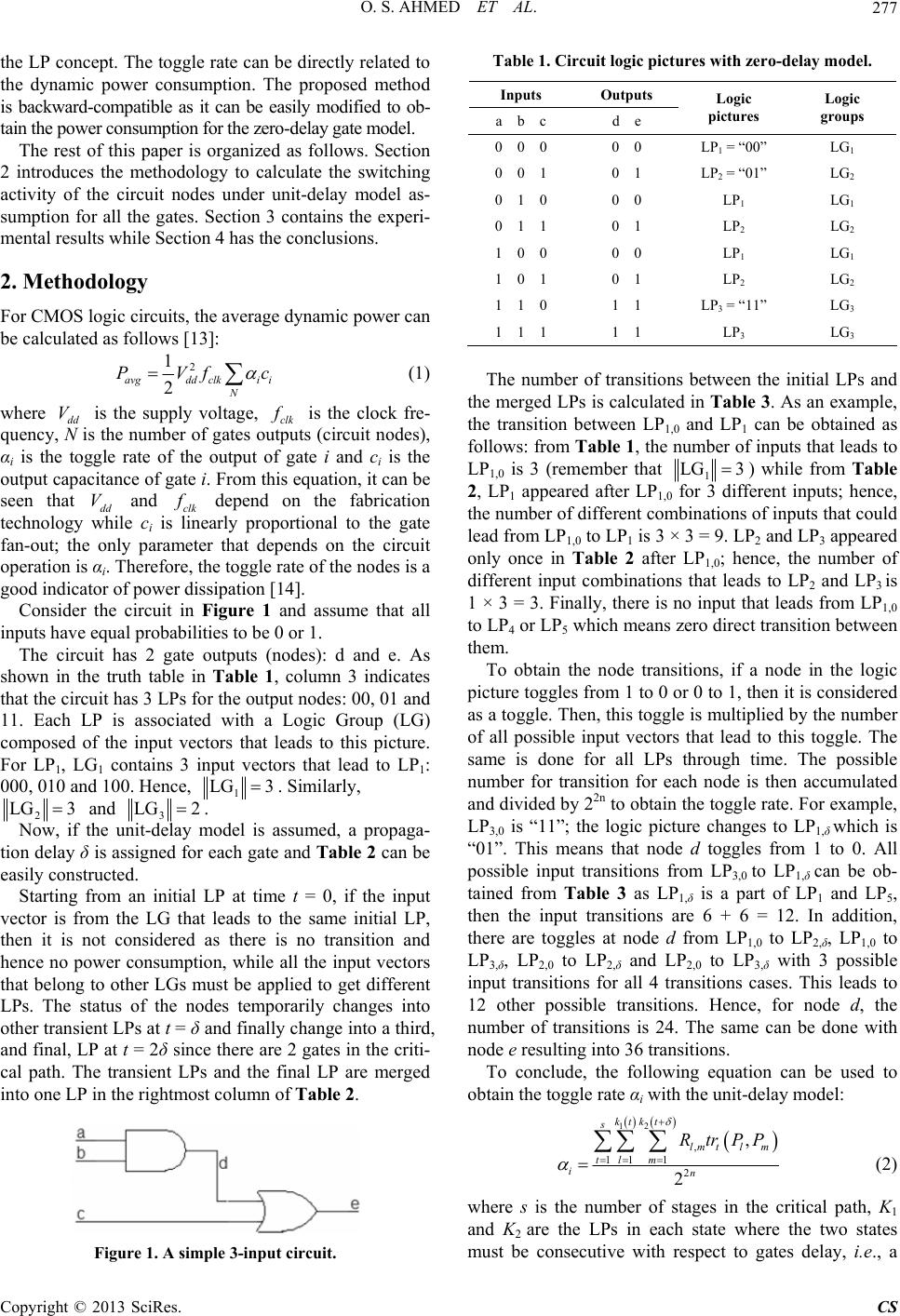 O. S. AHMED ET AL. 277 the LP concept. Th e toggle rate can be directly related to the dynamic power consumption. The proposed method is backward-compatible as it can be easily modified to ob- tain the power consumption for the zero-delay gate model. The rest of this paper is organized as follows. Section 2 introduces the methodology to calculate the switching activity of the circuit nodes under unit-delay model as- sumption for all the gates. Section 3 contains the experi- mental results while Section 4 has the conclusions. 2. Methodology For CMOS logic circuits, the average dynamic power can be calculated as follo ws [13]: 2 ddclki i N f c 1 2 avg PV V (1) where dd is the supply voltage, clk f is the clock fre- quency, N is the number of gates ou tputs (circuit nodes), αi is the toggle rate of the output of gate i and ci is the output capacitance of gate i. From this equation, it can be seen that dd V and clk f depend on the fabrication technology while ci is linearly proportional to the gate fan-out; the only parameter that depends on the circuit operation is αi. Therefore , th e tog g le rate of the nodes is a good indicator of power dissipation [14]. Consider the circuit in Figure 1 and assume that all inputs have equal probabilities to be 0 or 1. The circuit has 2 gate outputs (nodes): d and e. As shown in the truth table in Table 1, column 3 indicates that the circuit has 3 LPs for the output nodes: 00, 01 and 11. Each LP is associated with a Logic Group (LG) composed of the input vectors that leads to this picture. For LP1, LG1 contains 3 input vectors that lead to LP1: 000, 010 and 100. Hence, 1 LG 3. Similarly, 2 LG 3 and 3 LG 2. Now, if the unit-delay model is assumed, a propaga- tion delay δ is assigned for each gate and Table 2 can be easily constructed. Starting from an initial LP at time t = 0, if the input vector is from the LG that leads to the same initial LP, then it is not considered as there is no transition and hence no power consumption, while all the input vectors that belong to other LGs must be applied to get different LPs. The status of the nodes temporarily changes into other transient LPs at t = δ and finally change into a third, and final, LP at t = 2δ since there are 2 gates in the criti- cal path. The transient LPs and the final LP are merged into one LP in the rightmost column of Table 2. Figure 1. A simple 3-input circuit. Table 1. Circuit logic pictures with zero-delay model. Inputs Outputs a b c d e Logic pictures Logic groups 0 0 0 0 0 LP1 = “00” LG1 0 0 1 0 1 LP2 = “01” LG2 0 1 0 0 0 LP1 LG1 0 1 1 0 1 LP2 LG2 1 0 0 0 0 LP1 LG1 1 0 1 0 1 LP2 LG2 1 1 0 1 1 LP3 = “11” LG3 1 1 1 1 1 LP3 LG3 The number of transitions between the initial LPs and the merged LPs is calculated in Table 3. As an example, the transition between LP1,0 and LP1 can be obtained as follows: from Table 1, th e numb er of inpu ts th at lead s to LP1,0 is 3 (remember that 1) while from Table 2, LP1 appeared after LP1,0 for 3 different inputs; hence, the number of different combinations of inputs that could lead from LP1,0 to LP1 is 3 × 3 = 9. LP2 and LP3 appeared only once in Table 2 after LP1,0; hence, the number of different input combinations that leads to LP2 and LP3 is 1 × 3 = 3. Finally, there is no input that leads from LP1,0 to LP4 or LP5 which means zero direct transition between them. LG 3 To obtain the node transitions, if a node in the logic picture toggles from 1 to 0 or 0 to 1, then it is considered as a toggle. Then, this togg le is multiplied by the nu mber of all possible input vectors that lead to this toggle. The same is done for all LPs through time. The possible number for transition for each node is then accumulated and divided by 22n to obtain the toggle rate. Fo r example, LP3,0 is “11”; the logic picture changes to LP1,δ which is “01”. This means that node d toggles from 1 to 0. All possible input transitions from LP3,0 to LP1,δ can be ob- tained from Table 3 as LP1,δ is a part of LP1 and LP5, then the input transitions are 6 + 6 = 12. In addition, there are toggles at node d from LP1,0 to LP2,δ, LP1,0 to LP3,δ, LP2,0 to LP2,δ and LP2,0 to LP3,δ with 3 possible input transitions for all 4 transitions cases. This leads to 12 other possible transitions. Hence, for node d, the number of transitions is 24. The same can be done with node e resulting into 36 transitions. To conclude, the following equation can be used to obtain the toggle rate αi with the unit-delay model: 12 , 11 12 , 2 ktk t s lm tlm tl m in RtrPP (2) where s is the number of stages in the critical path, K1 and K2 are the LPs in each state where the two states ust be consecutive with respect to gates delay, i.e., a m Copyright © 2013 SciRes. CS 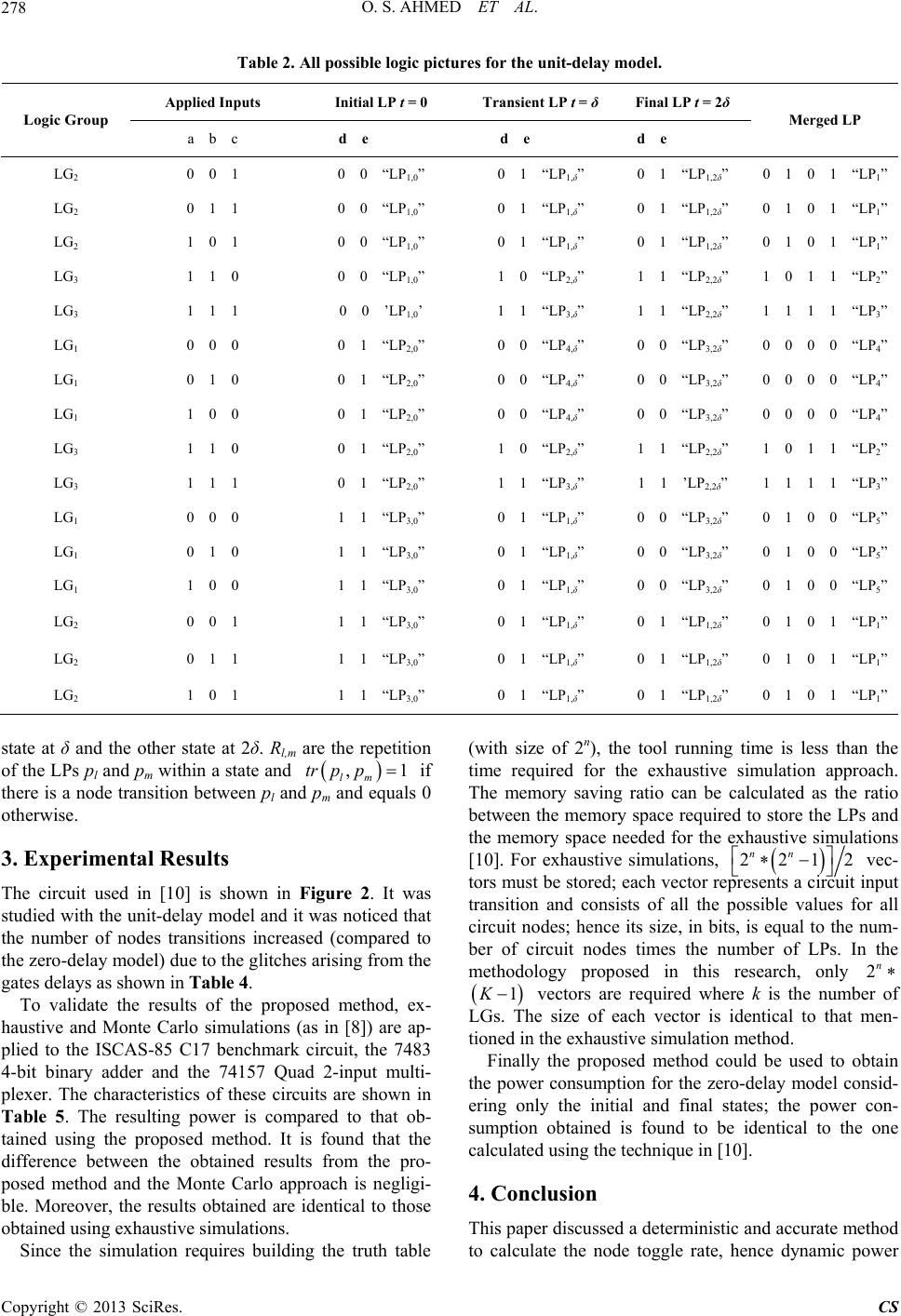 O. S. AHMED ET AL. Copyright © 2013 SciRes. CS 278 Table 2. All possible logic pictures for the unit-delay model. Applied InLP t = 2δ puts Initial LP t = 0 Transient LP t = δFinal Logic Group Merged LP a b c d e d e d e LG2 “LP1,0” P1,δ” “LP1,2δ” 0 1 0 1 “LP1”0 0 1 0 0 0 1 “L0 1 LG2 0 1 1 0 0 “LP1,0” 0 1 “LP1,δ” 0 1 “LP1,2δ” 0 1 0 1 “LP1” LG2 1 0 1 0 0 “LP1,0” 0 1 “LP1,δ” 0 1 “LP1,2δ” 0 1 0 1 “LP1” LG3 1 1 0 0 0 “LP1,0” 1 0 “LP2,δ” 1 1 “LP2,2δ” 1 0 1 1 “LP2” LG3 1 1 1 0 0 ’LP1,0’ 1 1 “LP3,δ” 1 1 “LP2,2δ” 1 1 1 1 “LP3” LG1 0 0 0 0 1 “LP2,0” 0 0 “LP4,δ” 0 0 “LP3,2δ” 0 0 0 0 “LP4” LG1 0 1 0 0 1 “LP2,0” 0 0 “LP4,δ” 0 0 “LP3,2δ” 0 0 0 0 “LP4” LG1 1 0 0 0 1 “LP2,0” 0 0 “LP4,δ” 0 0 “LP3,2δ” 0 0 0 0 “LP4” LG3 1 1 0 0 1 “LP2,0” 1 0 “LP2,δ” 1 1 “LP2,2δ” 1 0 1 1 “LP2” LG3 1 1 1 0 1 “LP2,0” 1 1 “LP3,δ” 1 1 ’LP2,2δ” 1 1 1 1 “LP3” LG1 0 0 0 1 1 “LP3,0” 0 1 “LP1,δ” 0 0 “LP3,2δ” 0 1 0 0 “LP5” LG1 0 1 0 1 1 “LP3,0” 0 1 “LP1,δ” 0 0 “LP3,2δ” 0 1 0 0 “LP5” LG1 1 0 0 1 1 “LP3,0” 0 1 “LP1,δ” 0 0 “LP3,2δ” 0 1 0 0 “LP5” LG2 0 0 1 1 1 “LP3,0” 0 1 “LP1,δ” 0 1 “LP1,2δ” 0 1 0 1 “LP1” LG2 0 1 1 1 1 “LP3,0” 0 1 “LP1,δ” 0 1 “LP1,2δ” 0 1 0 1 “LP1” LG2 1 0 1 1 1 “LP3,0” 0 1 “LP1,δ” 0 1 “LP1,2δ” 0 1 0 1 “LP1” ate at δ and the other state at 2δ. Rl,m are the repetition st of the LPs pl and pm within a state and ,1 lm tr pp if there is a node transition between pl and s 0 otherwise. 3. Experimental Results pm and equal Figure 2. It was (with size of 2n), the tool running time is less than the lation approach. The circuit used in [10] is shown in studied with the unit-delay mo del and it was noticed that the number of nodes transitions increased (compared to the zero-delay model) du e to the glitch es arising from the gates delays as shown in Table 4 . To validate the results of the proposed method, ex- haustive and Monte Carlo simulations (as in [8]) are ap- plied to the ISCAS-85 C17 benchmark circuit, the 7483 4-bit binary adder and the 74157 Quad 2-input multi- plexer. The characteristics of these circuits are shown in Table 5. The resulting power is compared to that ob- tained using the proposed method. It is found that the difference between the obtained results from the pro- posed method and the Monte Carlo approach is negligi- ble. Moreover, the results obtained are identical to those obtained usi ng exhaustive simulat i ons. Since the simulation requires building the truth table time required for the exhaustive simu The memory saving ratio can be calculated as the ratio between the memory space required to store the LPs and the memory space needed for the exhaustive simulations [10]. For exhaustive simulations, 2212 nn vec- tors must be stored; each vector represents a circuit input transition and consists of all the possible values for all circuit nodes; hence its size, in bit num- ber of circuit nodes times the number of LPs. In the methodology proposed in this research, only 2 s, is equal to the n 1 K vectors are required where k is the number of LGs. The size of each vector is identical to that men- tioned in the exhaustive simulation method. ly the proposed method could be used to obtain the power consumption for the zero-delay model consid- ering only the initial and final states; the power con- su Final d accurate method to calculate the node toggle rate, hence dynamic power mption obtained is found to be identical to the one calculated using the techn ique in [10]. 4. Conclusion This paper discussed a deterministic an 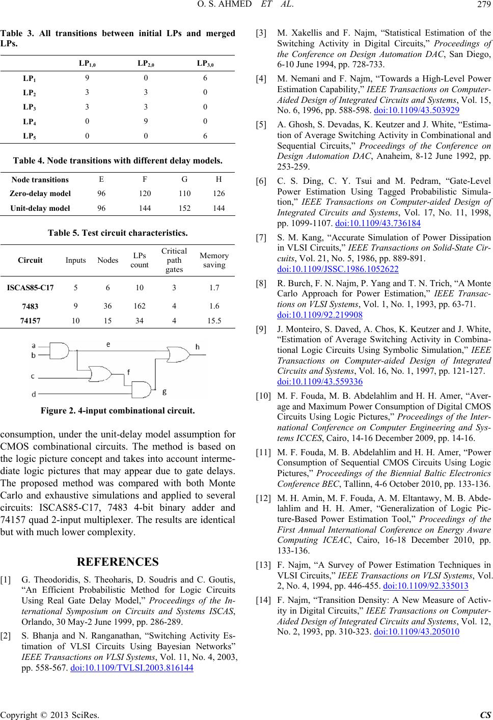 O. S. AHMED ET AL. 279 Table 3. All transitions between initial LPs and merged LPs. LP1,0 LP2,0 LP3,0 LP1 9 0 6 LP2 3 3 0 L3 P3 3 0 LP4 0 9 0 LP5 0 0 6 Ta. Node trans with dit delay m Nonsitions E G H ble 4sitionfferenodels. de tra F Zero-delay model 96 120 110 126 Unit-delay model 96 144 152 144 Tesit chterist Circuit Inputs Nodes L count Crit path Me saving Table 5.t circuaracics. Ps ical gates mory ISCAS85-C17 5 6 10 1.7 3 7483 9 36 162 4 1.6 74157 10 15 34 4 15.5 Figure 2. 4-input combinational circuit. consumption, under the unit-delay model assump CMOS coba e logic interme- . Soudris and C. Goutis, “An Efficient Probabilistic Method for Logic Circuits Using Real Geedings of the In- ternational Syd Systems ISCAS 4 tion f sed on or mbinational circuits. The method is picture concept and takes into account th diate logic pictures that may appear due to gate delays. The proposed method was compared with both Monte Carlo and exhaustive simulations and applied to several circuits: ISCAS85-C17, 7483 4-bit binary adder and 74157 quad 2-inpu t multiplexer. Th e results are identical but with much lower complexity. REFERENCES [1] G. Theodoridis, S. Theoharis, D ate Delay Model,” Proc mposium on Circuits an, Orlando, 30 May-2 June 1999, pp. 286-289. [2] S. Bhanja and N. Ranganathan, “Switching Activity Es- timation of VLSI Circuits Using Bayesian Networks” IEEE Transactions on VLSI Systems, Vol. 11, No. 4, 2003, pp. 558-567. doi:10.1109/TVLSI.2003.81614 an Diego, cuits and Systems, Vol. 15, [3] M. Xakellis and F. Najm, “Statistical Estimation of the Switching Activity in Digital Circuits,” Proceedings of the Conference on Design Automation DAC, S 6-10 June 1994, pp. 728-733. [4] M. Nemani and F. Najm, “Towards a High-Level Power Estimation Capability,” IEEE Transactions on Computer- Aided Design of Integrated Cir No. 6, 1996, pp. 588-598. doi:10.1109/43.503929 [5] A. Ghosh, S. Devadas, K. Keutzer and J. White, “Esti ma- tion of Average Switching Activity in Combinational and Sequential Circuits,” Proceedings of the Conference on E Transactions on Computer-aided Design of Design Automation DAC, Anaheim, 8-12 June 1992, pp. 253-259. [6] C. S. Ding, C. Y. Tsui and M. Pedram, “Gate-Level Power Estimation Using Tagged Probabilistic Simula- tion,” IEE Integrated Circuits and Systems, Vol. 17, No. 11, 1998, pp. 1099-1107. doi:10.1109/43.736184 [7] S. M. Kang, “Accurate Simulation of Power Dissipation in VLSI Circuits,” IEEE Transactions on Solid-State Cir- cuits, Vol. 21, No. 5, 1986, pp. 889-891. doi:10.1109/JSSC.1986.1052622 [8] R. Burch, F. N. Najm, P. Yang and T. N. Trich, “A Monte Carlo Approach for Power Estimation,” tions on VLSI Systems, Vol. 1, No. IEEE Transac- 1, 1993, pp. 63-71. doi:10.1109/92.219908 [9] J. Monteiro, S. Daved, A. Chos, K. Keutzer and J. White, “Estimation of Average Switching Activity in Combin tional Logic Circuits Usa- ing Symbolic Simulation,” IEEE Transactions on Computer-aided Design of Integrated Circuits and Systems, Vol. 16, No. 1, 1997, pp. 121-127. doi:10.1109/43.559336 [10] M. F. Fouda, M. B. Abdelahlim and H. H. Amer, “Aver- age and Maximum Power Consumption of Digital CMOS Circuits Using Logic Pic tures,” Proceedings of the Inter- ics 994, pp. 446-455. doi:10.1109/92.335013 national Conference on Computer Engineering and Sys- tems ICCES, Cairo, 14-16 December 2009, pp. 14-16. [11] M. F. Fouda, M. B. Abdelahlim and H. H. Amer, “Power Consumption of Sequential CMOS Circuits Using Logic Pictures,” Proceedings of the Biennial Baltic Electron Conference BEC, Tallinn, 4-6 October 2010, pp. 133-136. [12] M. H. Amin, M. F. Fouda, A. M. Eltantawy, M. B. Abde- lahlim and H. H. Amer, “Generalization of Logic Pic- ture-Based Power Estimation Tool,” Proceedings of the First Annual International Conference on Energy Aware Computing ICEAC, Cairo, 16-18 December 2010, pp. 133-136. [13] F. Najm, “A Survey of Power Estimation Techniques in VLSI Circuits,” IEEE Transactions on VLSI Systems, Vol. 2, No. 4, 1 l. 12, [14] F. Najm, “Transition Density: A New Measure of Activ- ity in Digital Circuits,” IEEE Transactions on Computer- Aided Design of Integrated Circuits and Systems, Vo No. 2, 1993, pp. 310-323. doi:10.1109/43.205010 Copyright © 2013 SciRes. CS |