

Paper Menu >>
Journal Menu >>
 Circuits and Systems, 2013, 4, 269-275 http://dx.doi.org/10.4236/cs.2013.43036 Published Online July 2013 (http://www.scirp.org/journal/cs) Design of Low Voltage, Low Power (IF) Amplifier Based-On MOSFET Darlington Configuration Hassan Jassim Motlak Electrical Department, College of Engineering, Babylon University, Babylon, Iraq Email: [email protected] Received April 20, 2013; revised May 21, 2013; accepted May 30, 2013 Copyright © 2013 Hassan Jassim Motlak. This is an open access article distributed under the Creative Commons Attribution License, which permits unrestricted use, distribution, and reproduction in any medium, provided the original work is properly cited. ABSTRACT This paper presents a different approach of Intermediate Frequency (IF) amplifier using 0.18 μm MIETEC technology channel length of MOSFET Darlington transistors. In contrast to Bipolar conventional Darlington pair, a MOSFET Darlington configuration is employed to reduce supply voltage (VDD) and DC consumption power (Pc). The frequency response parameters of the proposed design such as bandwidth, gain bandwidth product, input/output noises and noise figure (NF) are improved in proposed (IF) amplifier. Moreover, a dual-input and dual-output (DIDO) IF amplifier con- structed from two symmetrical single input and single output (SISO) (IF) amplifier is proposed too. The idea is to achieve improved bandwidth, and flat response, because these parameters are very important in high frequency applica- tions. Simulation results that obtained by P-SPICE program are 1.2 GHz Bandwidth (BW), 3.4 GHz (gain bandwidth product), 0.5 mW DC consumption power (Pc) and the low total output noise is 12 nVHz with 1.2 V single supply voltage. Keywords: N(IF) Amplifier; MOSFET Darlington Configuration; Dual-Input and Dual-Output (DIDO) IF Amplifier 1. Introduction The communication market has been growing very fast during the last decade especially for mobile communica- tion systems. The low power, low voltage and low noise (IF) amplifier is one of the most essential building blocks in the communication circuits. It can be found in the al- most of the commercial and military receivers [1]. Sev- eral architectures of (IF) amplifier such as operational amplifier and Darlington pairs have been reported [2,3]. The most common used Darlington pair consists of an emitter-follower and a common-emitter bipolar transis- tors [3,4]. However, a major drawback is encountered with its performance. At higher frequencies its response becomes poorer than that of a single transistor amplifier [5]. To overcome this problem, a number of modifica- tions are attempted in Darlington pair amplifiers either by adding some extra biasing resistances in the circuit or by using Triple Darlington topology the earlier published Darlington amplifiers [5-8]. All previous work still suf- fers from high DC consumption power due to high value of collector current, high noise and limitation in band- width. In this paper, a simple circuitry high performance single input and single output (SISO) (IF) amplifier based on (0.18 um) channel length MOSFETs Darlington configuration is proposed. The proposed amplifier used small channel-length (0.18 μm) to overcome the prob- lems in consumption power, limitation in bandwidth, and inter-electrode capacitances. Because the small channel length of MOSFETs reduced the effect of inter-electrode capacitances at high frequency operation of MOSFETs. Besides that the reducing channel length will reduce the value of threshold voltage of MOSFETs and capable the designer to use small value of supply voltage and supply current. A dual-input and dual-output (DIDO) (IF) am- plifier constructed from two symmetrical (SISO) (IF) amplifiers is proposed in this approach. The proposed dual-input and dual output (DIDO) (IF) amplifier is im- portant in vast area of mobile applications such as multi- band, wideband, and high-isolation multiple-input multi- ple-output techniques. 2. Design of Single Input and Single Output (SISO) IF Amplifier Figure 1 shows the schematic circuit diagram of the proposed (IF) amplifier based on MOSFET Darlington configuration. The proposed amplifier constructed from two stages using NMOS transistors, biasing voltage and biasing resistors. The values of biasing resistors includ- C opyright © 2013 SciRes. CS 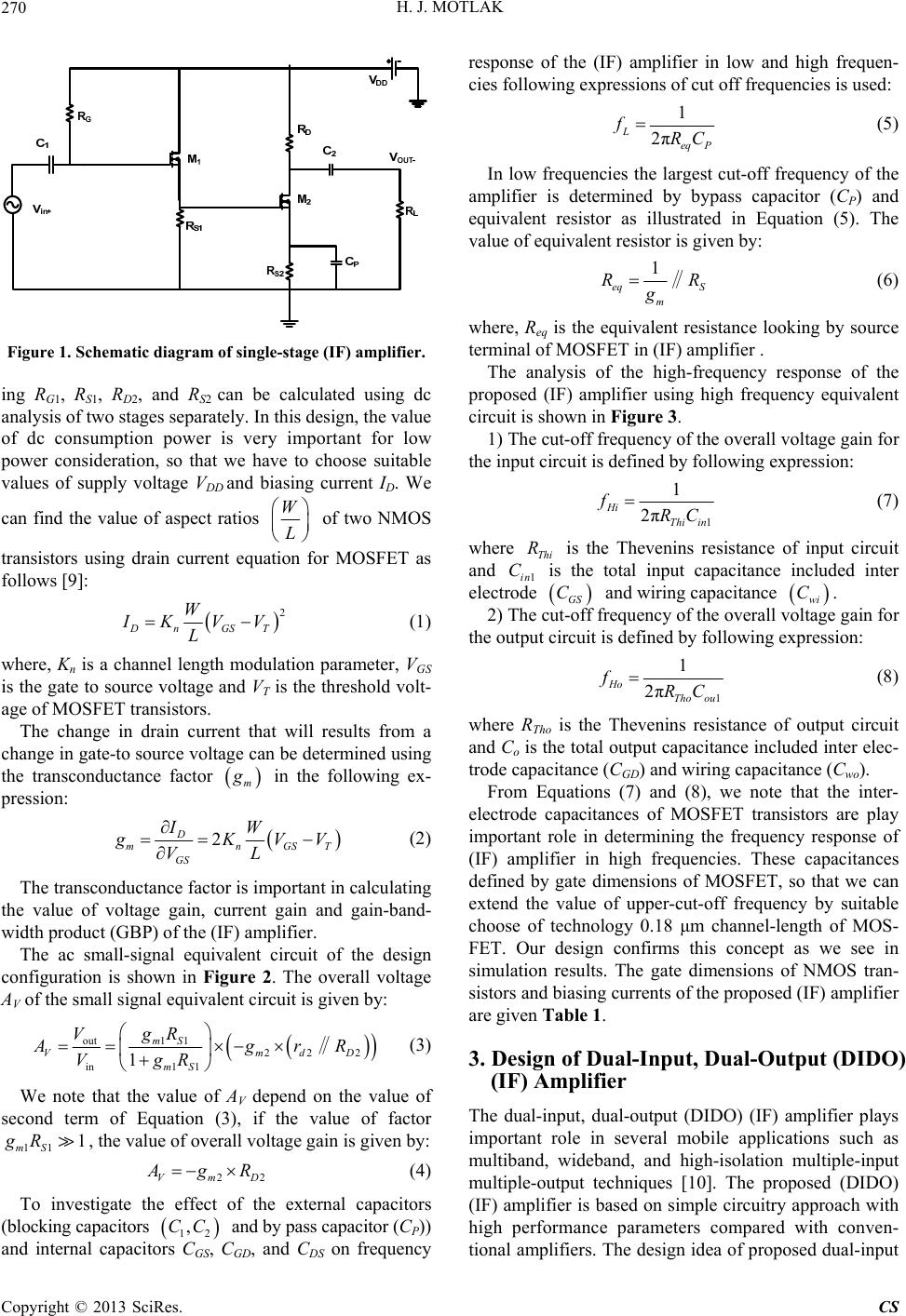 H. J. MOTLAK 270 Figure 1. Schematic diagram of single-stage (IF) amplifier. ing RG1, RS1, RD2, and RS2 can be calculated using dc analysis of two stages separately. In this design, the value of dc consumption power is very important for low power consideration, so that we have to choose suitable values of supply voltage VDD and biasing current ID. We can find the value of aspect ratios W L of two NMOS transistors using drain current equation for MOSFET as follows [9]: 2 GST W Dn I KVV L (1) where, Kn is a channel length modulation parameter, VGS is the gate to source voltage and VT is the threshold volt- age of MOSFET transistors. The change in drain current that will results from a change in gate-to source voltage can be determined using the transconductance factor m g in the following ex- pression: GST IW 2 D mn GS g KVV VL (2) The transconductance factor is important in calculating the value of voltage gain, current gain and gain-band- width product (GBP) of the (IF) amplifier. The ac small-signal equivalent circuit of the design configuration is shown in Figure 2. The overall voltage AV of the small signal equivalent circuit is given by: 22 2dD rR ‖ 11 1 mS gR 22VmD out1 1 in1 1 1 mS Vm mS VgR Ag VgR (3) We note that the value of AV depend on the value of second term of Equation (3), if the value of factor , the value of overall voltage gain is given by: A gR (4) To investigate the effect of the external capacitors (blocking capacitors 1 and by pass capacitor (CP)) and internal capacitors CGS, CGD, and CDS on frequency response of the (IF) amplifier in low and high frequen- cies following expressions of cut off frequencies is used: 2 ,CC 1 2π Leq P fRC (5) In low frequencies the largest cut-off frequency of the amplifier is determined by bypass capacitor (CP) and equivalent resistor as illustrated in Equation (5). The value of equivalent resistor is given by: 1 eq S m RR g ‖ (6) where, Req is the equivalent resistance looking by source terminal of MOSFET in (IF) amplifier . The analysis of the high-frequency response of the proposed (IF) amplifier using high frequency equivalent circuit is shown in Figure 3. 1) The cut-off frequency of the overall voltage gain for the input circuit is defined by following expression: 1 1 2π Hi Thi in fRC R C (7) where Thi is the Thevenins resistance of input circuit and 1in is the total input capacitance included inter electrode GS wi 2) The cut-off frequency of the overall voltage gain for the output circuit is defined by following expression: C C and wiring capacitance . 1 1 2π Ho Tho ou fRC (8) where RTho is the Thevenins resistance of output circuit and Co is the total output capacitance included inter elec- trode capacitance (CGD) and wiring capacitance (Cwo). From Equations (7) and (8), we note that the inter- electrode capacitances of MOSFET transistors are play important role in determining the frequency response of (IF) amplifier in high frequencies. These capacitances defined by gate dimensions of MOSFET, so that we can extend the value of upper-cut-off frequency by suitable choose of technology 0.18 μm channel-length of MOS- FET. Our design confirms this concept as we see in simulation results. The gate dimensions of NMOS tran- sistors and biasing currents of the proposed (IF) amplifier are given Table 1. 3. Design of Dual-Input, Dual-Output (DIDO) (IF) Amplifier The dual-input, dual-output (DIDO) (IF) amplifier plays important role in several mobile applications such as multiband, wideband, and high-isolation multiple-input multiple-output techniques [10]. The proposed (DIDO) (IF) amplifier is based on simple circuitry approach with high performance parameters compared with conven- ional amplifiers. The design idea of proposed dual-input t Copyright © 2013 SciRes. CS 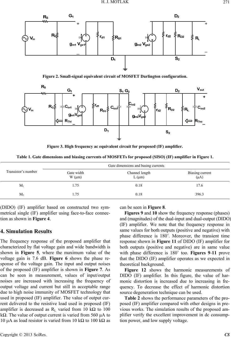 H. J. MOTLAK Copyright © 2013 SciRes. CS 271 Figure 2. Small-signal equivalent circuit of MOSFET Darlington configuration. Figure 3. High frequency ac equivalent circuit for proposed (IF) amplifier. Table 1. Gate dimensions and biasing currents of MOSFETs for proposed (SISO) (IF) amplifier in Figure 1. Gate dimensions and basing currents Transistor’s number Gate width W (μm) Channel length L (μm) Biasing current (μA) M1 1.75 0.18 17.6 M2 1.75 0.18 396.3 (DIDO) (IF) amplifier based on constructed two sym- metrical single (IF) amplifier using face-to-face connec- tion as shown in Figure 4. 4. Simulation Results The frequency response of the proposed amplifier that characterized by flat voltage gain and wide bandwidth is shown in Figure 5, where the maximum value of the voltage gain is 7.6 dB. Figure 6 shows the phase re- sponse of the voltage gain. The input and output noises of the proposed (IF) amplifier is shown in Figure 7. As can be seen in measurement, values of input/output noises are increased with increasing the frequency of output voltage and current but still in acceptable range due to high noise immunity of MOSFET technology that used in proposed (IF) amplifier. The value of output cur- rent delivered to the resistive load used in proposed (IF) amplifier is decreased as RL varied from 10 kΩ to 100 kΩ. The value of output current is varied from 560 μA to 10 μA as load resistor is varied from 10 kΩ to 100 kΩ as can be seen in Figure 8. Figures 9 and 10 show the frequency response (phases) and (magnitudes) of the dual-input and dual-output (DIDO) (IF) amplifier. We note that the frequency response in same values for both outputs (positive and negative) with phase difference is 180˚. Moreover, the transient time response shown in Figure 11 of DIDO (IF) amplifier for both outputs (positive and negative) are in same value with phase difference is 180˚ too. Figures 9-11 prove that the DIDO (IF) amplifier operates as we expected in theoretical background. Figure 12 shows the harmonic measurements of DIDO (IF) amplifier. In this figure, the value of har- monic distortion is increased due to increasing in fre- quency. To decrease the effect of harmonic distortion source degeneration technique can be used. Table 2 shows the performance parameters of the pro- posed (IF) amplifier compared with other designs in pre- vious works. The simulation results of the proposed am- plifier verify the excellent improvement in dc consump- tion power, and low supply voltage. 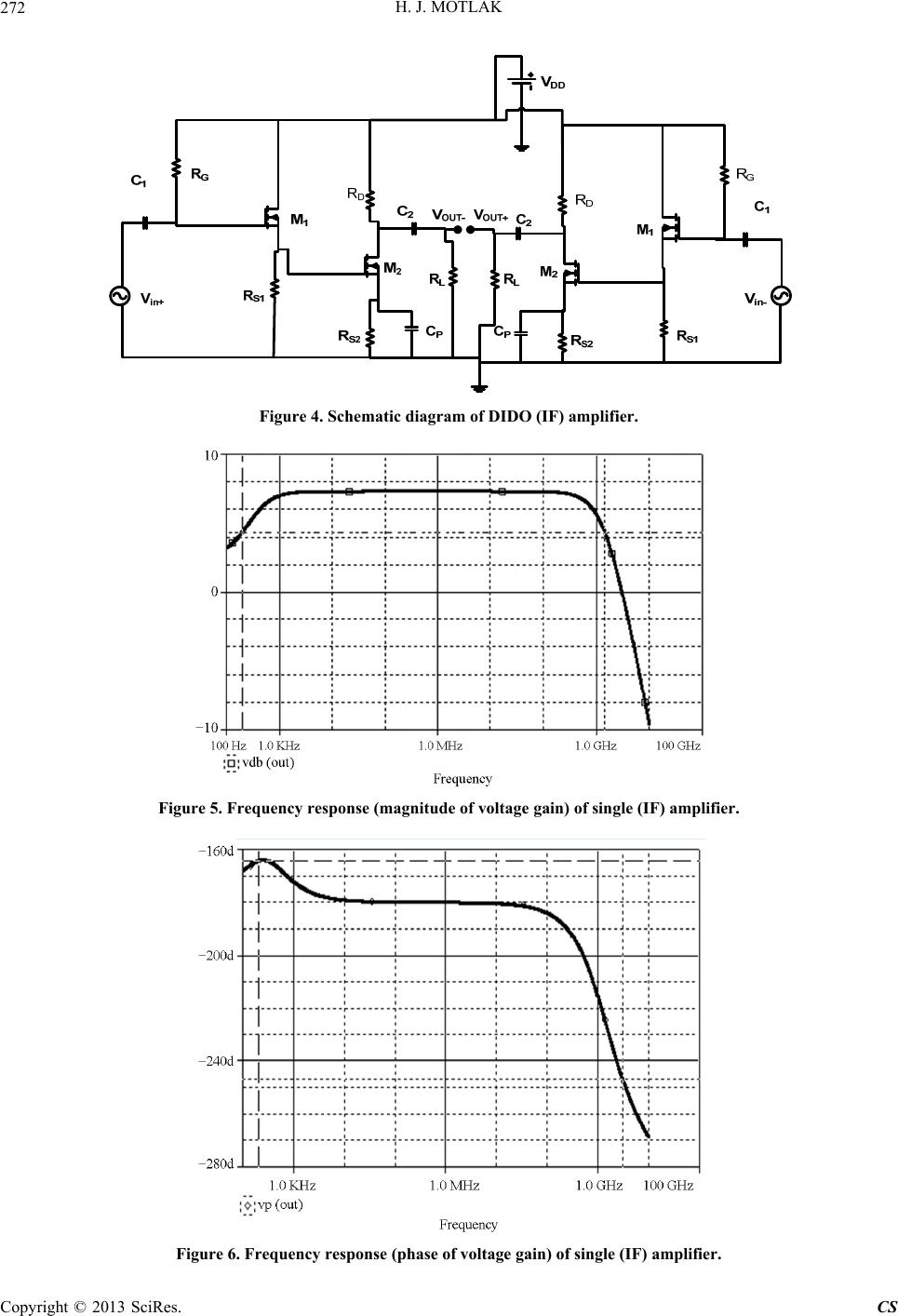 H. J. MOTLAK 272 Figure 4. Schematic diagram of DIDO (IF) amplifier. Figure 5. Frequency response (magnitude of voltage gain) of single (IF) amplifier. Figure 6. Frequency response (phase of voltage gain) of single (IF) amplifier. Copyright © 2013 SciRes. CS  H. J. MOTLAK 273 Figure 7. Input and output noises of proposed (IF) amplifier. Figure 8. Frequency response of output current as RL is varied from 10 kΩ to 100 kΩ of the prosed (IF) amplifier. op Figure 9. Frequency responses (phases) of positive and negative outputs of the proposed DIDO (IF) amplifier. Copyright © 2013 SciRes. CS 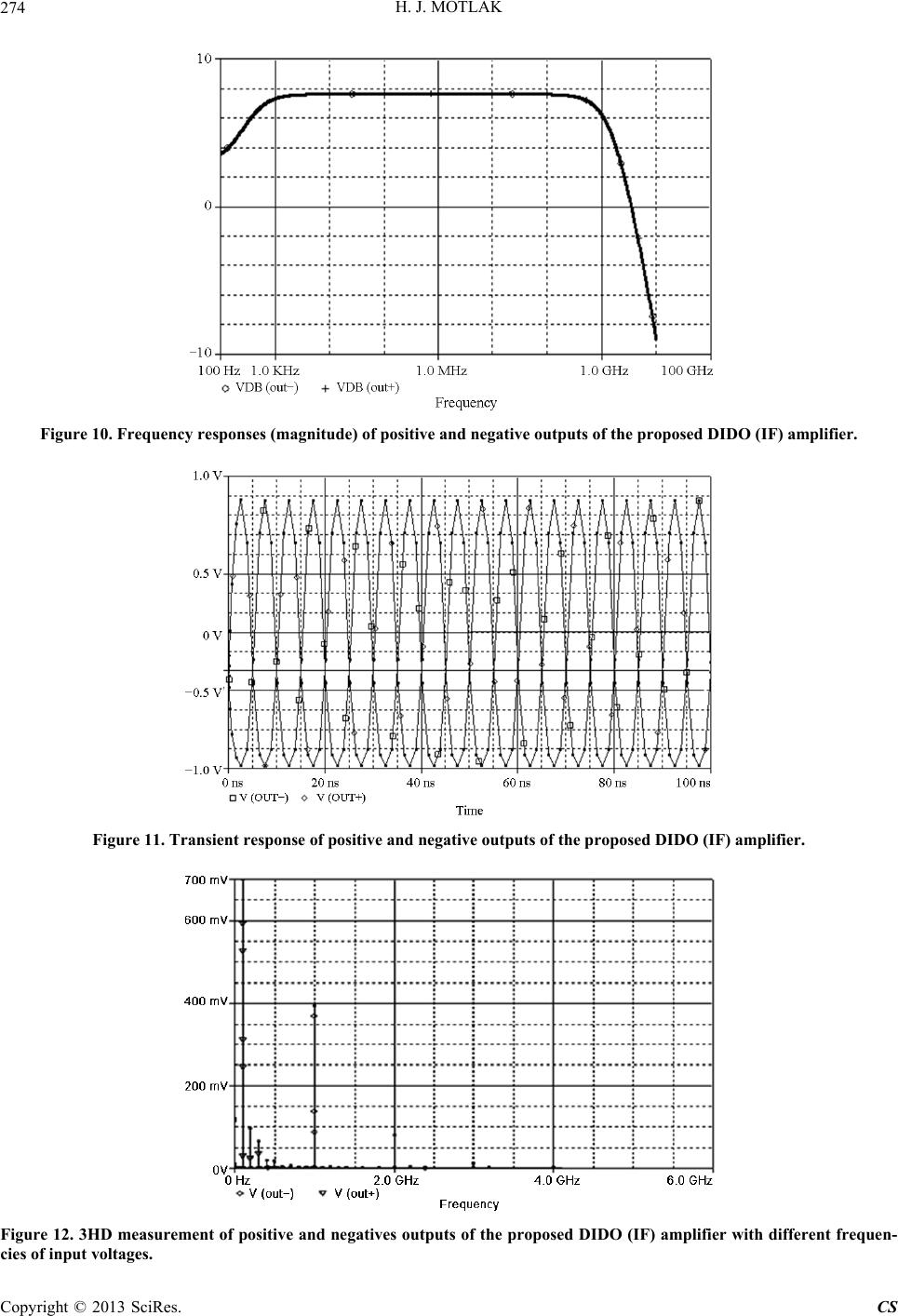 H. J. MOTLAK 274 Figure 10. Frequency responses (magnitude) of positive and negative outputs of the proposed DIDO (IF) amplifier. Figure 11. Transient response of positive and negative outputs of the proposed DIDO (IF) amplifier. Figure 12. 3HD measurement of positive and negatives outputs of the proposed DIDO (IF) amplifiwith different frequen-er cies of input voltages. Copyright © 2013 SciRes. CS 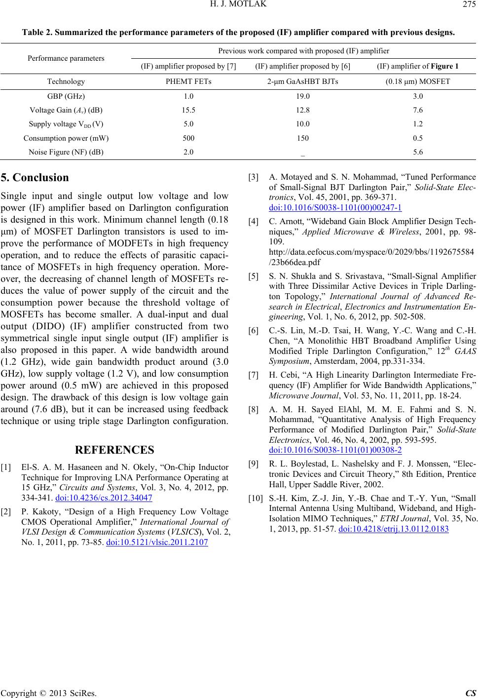 H. J. MOTLAK Copyright © 2013 SciRes. CS 275 ized the performance parameters of the proposed (IF) amplifier compared with previous designs. Previous work compared with proposed (IF) amplifier Table 2. Summar Performance parameters (IF) amplifier proposed mplifier of Figure 1 by [7] (IF) amplifier proposed by [6] (IF) a Technology PHEMT FETs 2-μm GaAsHBT BJTs (0.18 μm) MOSFET GBP (GHz) 1.0 19.0 3.0 Volta dB) C ge Gain (Av) (15.5 12.8 7.6 Supply voltage VDD (V) 5.0 10.0 1.2 onsumption power (mW)500 150 0.5 Noise Figure (NF) (dB) 2.0 _ 5.6 ngle output low voltage and low [1] El-S. A. M. H 5. Conclusion Single input and si power (IF) amplifier based on Darlington configuration is designed in this work. Minimum channel length (0.18 μm) of MOSFET Darlington transistors is used to im- prove the performance of MODFETs in high frequency operation, and to reduce the effects of parasitic capaci- tance of MOSFETs in high frequency operation. More- over, the decreasing of channel length of MOSFETs re- duces the value of power supply of the circuit and the consumption power because the threshold voltage of MOSFETs has become smaller. A dual-input and dual output (DIDO) (IF) amplifier constructed from two symmetrical single input single output (IF) amplifier is also proposed in this paper. A wide bandwidth around (1.2 GHz), wide gain bandwidth product around (3.0 GHz), low supply voltage (1.2 V), and low consumption power around (0.5 mW) are achieved in this proposed design. The drawback of this design is low voltage gain around (7.6 dB), but it can be increased using feedback technique or using triple stage Darlington configuration. REFERENCES asaneen and N. Okely, “On-Chip Inductor Technique for Improving LNA Performance Operating at 15 GHz,” Circuits and Systems, Vol. 3, No. 4, 2012, pp. 334-341. doi:10.4236/cs.2012.34047 [2] P. Kakoty, “Design of a High Frequency Low Voltage CMOS Operational Amplifier,” International Journal of VLSI Design & Communication Systems (VLSICS), Vol. 2, No. 1, 2011, pp. 73-85. doi:10.5121/vlsic.2011.2107 [3] A. Motayed and S. N. Mohammad, “Tuned Performance of Small-Signal BJT Darlington Pair,” Solid-State Elec- tronics, Vol. 45, 2001, pp. 369-371. doi:10.1016/S0038-1101(00)00247-1 lifier Design Tech- data.eefocus.com/myspace/0/2029/bbs/1192675584 d S. Srivastava, “Small-Signal Amplifier g and C.-H. mediate Fre- N. [4] C. Arnott, “Wideband Gain Block Amp niques,” Applied Microwave & Wireless, 2001, pp. 98- 109. http:// /23b66dea.pdf [5] S. N. Shukla an with Three Dissimilar Active Devices in Triple Darling- ton Topology,” International Journal of Advanced Re- search in Electrical, Electronics and Instrumentation En- gineering, Vol. 1, No. 6, 2012, pp. 502-508. [6] C.-S. Lin, M.-D. Tsai, H. Wang, Y.-C. Wan Chen, “A Monolithic HBT Broadband Amplifier Using Modified Triple Darlington Configuration,” 12th GAAS Symposium, Amsterdam, 2004, pp.331-334. [7] H. Cebi, “A High Linearity Darlington Inter quency (IF) Amplifier for Wide Bandwidth Applications,” Microwave Journal, Vol. 53, No. 11, 2011, pp. 18-24. [8] A. M. H. Sayed ElAhl, M. M. E. Fahmi and S. Mohammad, “Quantitative Analysis of High Frequency Performance of Modified Darlington Pair,” Solid-State Electronics, Vol. 46, No. 4, 2002, pp. 593-595. doi:10.1016/S0038-1101(01)00308-2 [9] R. L. Boylestad, L. Nashelsky and F. J. Monssen, “Elec- and T.-Y. Yun, “Small tronic Devices and Circuit Theory,” 8th Edition, Prentice Hall, Upper Saddle River, 2002. [10] S.-H. Kim, Z.-J. Jin, Y.-B. Chae Internal Antenna Using Multiband, Wideband, and High- Isolation MIMO Techniques,” ETRI Journal, Vol. 35, No. 1, 2013, pp. 51-57. doi:10.4218/etrij.13.0112.0183 |