

Paper Menu >>
Journal Menu >>
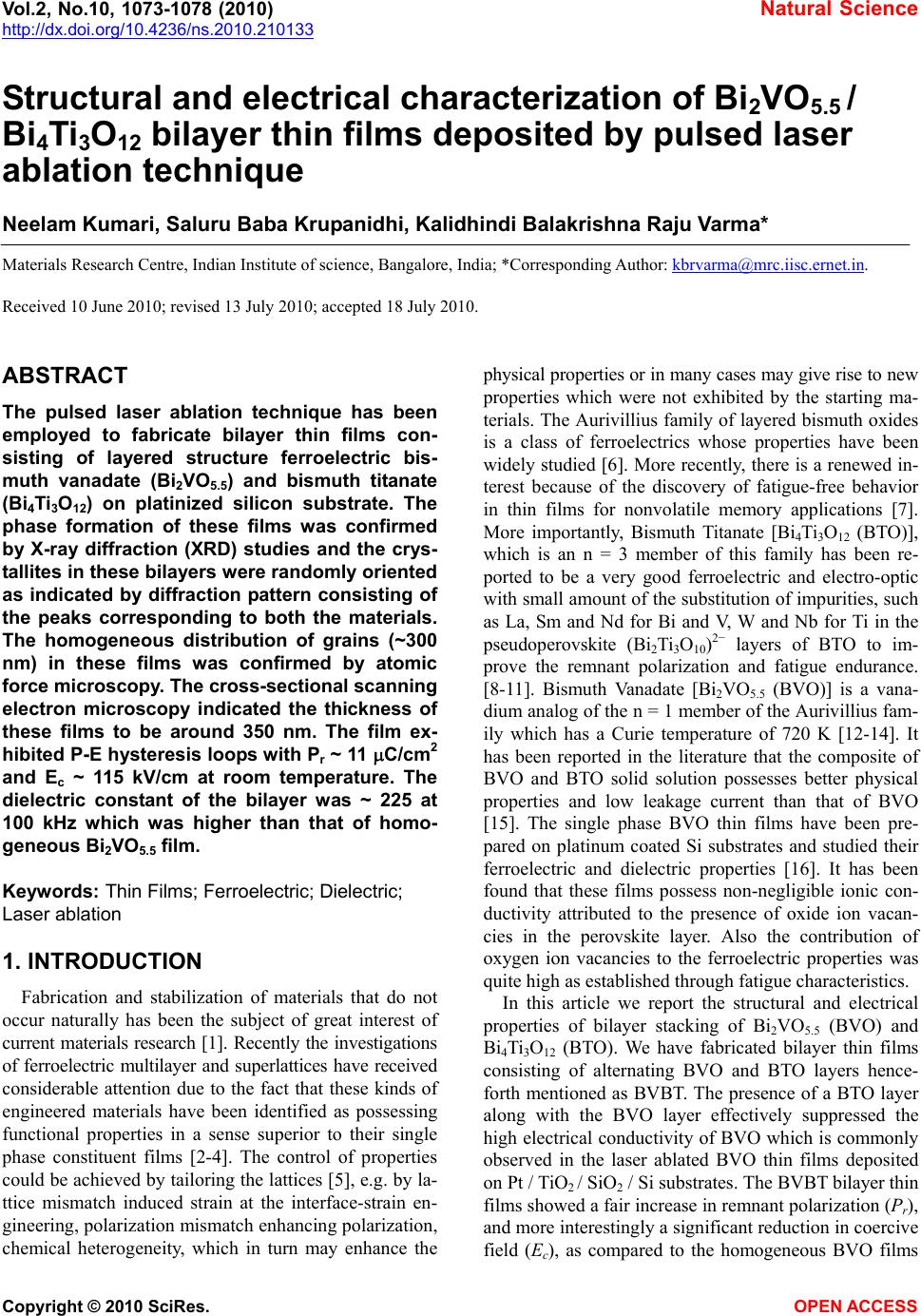 Vol.2, No.10, 1073-1078 (2010) Natural Science http://dx.doi.org/10.4236/ns.2010.210133 Copyright © 2010 SciRes. OPEN ACCESS Structural and electrical characterization of Bi2VO5.5 / Bi4Ti3O12 bilayer thin films deposited by pulsed laser ablation technique Neelam Kumari, Saluru Baba Krupanidhi, Kalidhindi Balakrishna Raju Varma* Materials Research Centre, Indian Institute of science, Bangalore, India; *Corresponding Author: [email protected]. Received 10 June 2010; revised 13 July 2010; accepted 18 July 2010. ABSTRACT The pulsed laser ablation technique has been employed to fabricate bilayer thin films con- sisting of layered structure ferroelectric bis- muth vanadate (Bi2VO5.5) and bismuth titanate (Bi4Ti3O12) on platinized silicon substrate. The phase formation of these films was confirmed by X-ray diffraction (XRD) studies and the crys- tallites in these bilayers were randomly oriented as indicated by diffraction pattern consisting of the peaks corresponding to both the materials. The homogeneous distribution of grains (~300 nm) in these films was confirmed by atomic force microscopy. The cross-sectional scanning electron microscopy indicated the thickness of these films to be around 350 nm. The film ex- hibited P-E hysteresis loops with Pr ~ 11 C/cm2 and Ec ~ 115 kV/cm at room temperature. The dielectric constant of the bilayer was ~ 225 at 100 kHz which was higher than that of homo- geneous Bi2VO5.5 film. Keywords: Thin Films; Ferroelectric; Dielectric; Laser ablation 1. INTRODUCTION Fabrication and stabilization of materials that do not occur naturally has been the subject of great interest of current materials research [1]. Recently the investigations of ferroelectric multilayer and superlattices have received considerable attention due to the fact that these kinds of engineered materials have been identified as possessing functional properties in a sense superior to their single phase constituent films [2-4]. The control of properties could be achieved by tailoring the lattices [5], e.g. by la- ttice mismatch induced strain at the interface-strain en- gineering, polarization mismatch enhancing polarization, chemical heterogeneity, which in turn may enhance the physical properties or in many cases may give rise to new properties which were not exhibited by the starting ma- terials. The Aurivillius family of layered bismuth oxides is a class of ferroelectrics whose properties have been widely studied [6]. More recently, there is a renewed in- terest because of the discovery of fatigue-free behavior in thin films for nonvolatile memory applications [7]. More importantly, Bismuth Titanate [Bi4Ti3O12 (BTO)], which is an n = 3 member of this family has been re- ported to be a very good ferroelectric and electro-optic with small amount of the substitution of impurities, such as La, Sm and Nd for Bi and V, W and Nb for Ti in the pseudoperovskite (Bi2Ti3O10)2− layers of BTO to im- prove the remnant polarization and fatigue endurance. [8-11]. Bismuth Vanadate [Bi2VO5.5 (BVO)] is a vana- dium analog of the n = 1 member of the Aurivillius fam- ily which has a Curie temperature of 720 K [12-14]. It has been reported in the literature that the composite of BVO and BTO solid solution possesses better physical properties and low leakage current than that of BVO [15]. The single phase BVO thin films have been pre- pared on platinum coated Si substrates and studied their ferroelectric and dielectric properties [16]. It has been found that these films possess non-negligible ionic con- ductivity attributed to the presence of oxide ion vacan- cies in the perovskite layer. Also the contribution of oxygen ion vacancies to the ferroelectric properties was quite high as established through fatigue characteristics. In this article we report the structural and electrical properties of bilayer stacking of Bi2VO5.5 (BVO) and Bi4Ti3O12 (BTO). We have fabricated bilayer thin films consisting of alternating BVO and BTO layers hence- forth mentioned as BVBT. The presence of a BTO layer along with the BVO layer effectively suppressed the high electrical conductivity of BVO which is commonly observed in the laser ablated BVO thin films deposited on Pt / TiO2 / SiO2 / Si substrates. The BVBT bilayer thin films showed a fair increase in remnant polarization (Pr), and more interestingly a significant reduction in coercive field (Ec), as compared to the homogeneous BVO films 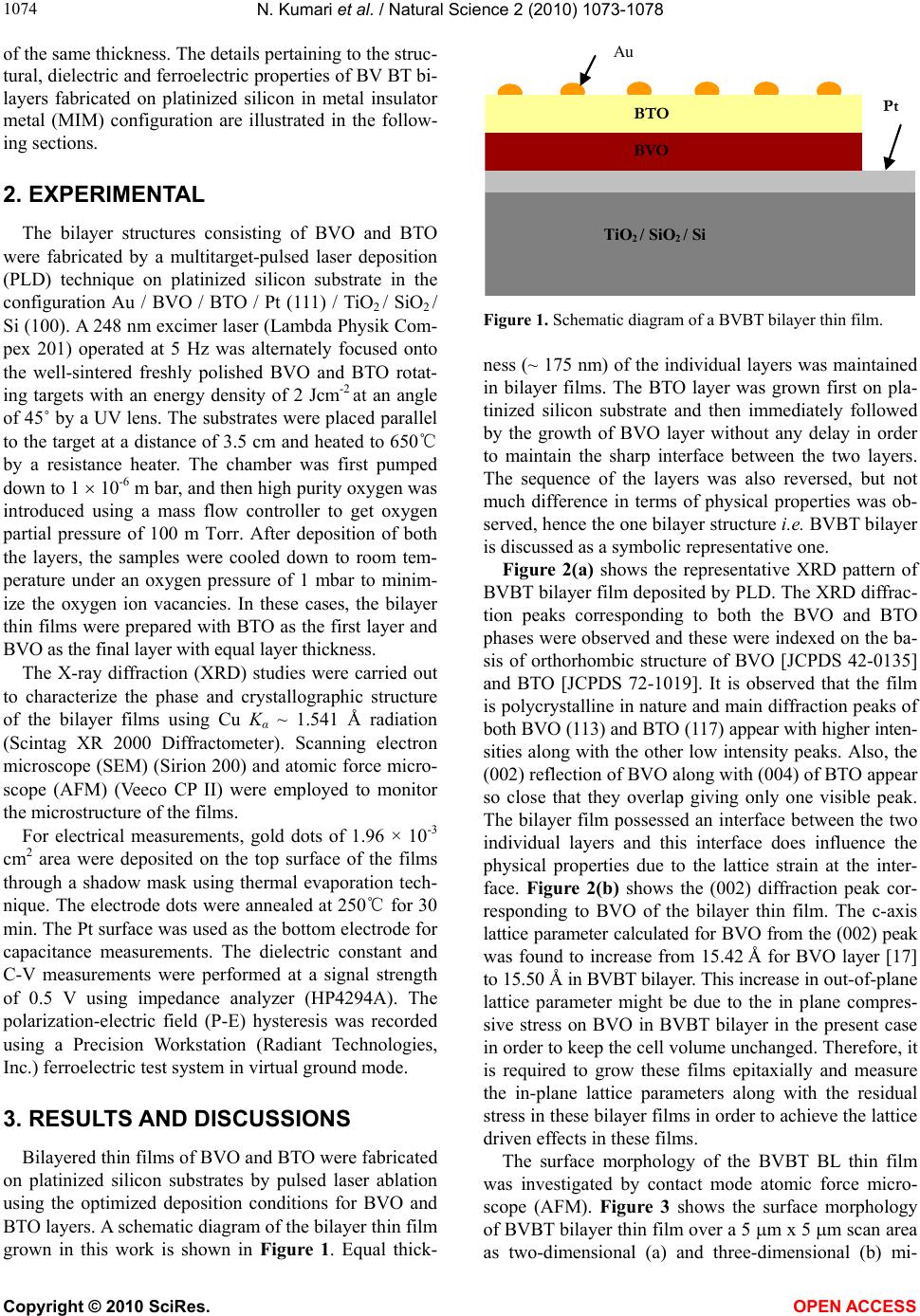 N. Kumari et al. / Natural Science 2 (2010) 1073-1078 Copyright © 2010 SciRes. OPEN ACCESS 1074 of the same thickness. The details pertaining to the struc- tural, dielectric and ferroelectric properties of BV BT bi- layers fabricated on platinized silicon in metal insulator metal (MIM) configuration are illustrated in the follow- ing sections. 2. EXPERIMENTAL The bilayer structures consisting of BVO and BTO were fabricated by a multitarget-pulsed laser deposition (PLD) technique on platinized silicon substrate in the configuration Au / BVO / BTO / Pt (111) / TiO2 / SiO2 / Si (100). A 248 nm excimer laser (Lambda Physik Com- pex 201) operated at 5 Hz was alternately focused onto the well-sintered freshly polished BVO and BTO rotat- ing targets with an energy density of 2 Jcm-2 at an angle of 45˚ by a UV lens. The substrates were placed parallel to the target at a distance of 3.5 cm and heated to 650℃ by a resistance heater. The chamber was first pumped down to 1 10-6 m bar, and then high purity oxygen was introduced using a mass flow controller to get oxygen partial pressure of 100 m Torr. After deposition of both the layers, the samples were cooled down to room tem- perature under an oxygen pressure of 1 mbar to minim- ize the oxygen ion vacancies. In these cases, the bilayer thin films were prepared with BTO as the first layer and BVO as the final layer with equal layer thickness. The X-ray diffraction (XRD) studies were carried out to characterize the phase and crystallographic structure of the bilayer films using Cu Kα ~ 1.541 Å radiation (Scintag XR 2000 Diffractometer). Scanning electron microscope (SEM) (Sirion 200) and atomic force micro- scope (AFM) (Veeco CP II) were employed to monitor the microstructure of the films. For electrical measurements, gold dots of 1.96 × 10⁻³ cm2 area were deposited on the top surface of the films through a shadow mask using thermal evaporation tech- nique. The electrode dots were annealed at 250℃ for 30 min. The Pt surface was used as the bottom electrode for capacitance measurements. The dielectric constant and C-V measurements were performed at a signal strength of 0.5 V using impedance analyzer (HP4294A). The polarization-electric field (P-E) hysteresis was recorded using a Precision Workstation (Radiant Technologies, Inc.) ferroelectric test system in virtual ground mode. 3. RESULTS AND DISCUSSIONS Bilayered thin films of BVO and BTO were fabricated on platinized silicon substrates by pulsed laser ablation using the optimized deposition conditions for BVO and BTO layers. A schematic diagram of the bilayer thin film grown in this work is shown in Figure 1. Equal thick- TiO 2 / SiO 2 / Si BTO BVO Pt Au Figure 1. Schematic diagram of a BVBT bilayer thin film. ness (~ 175 nm) of the individual layers was maintained in bilayer films. The BTO layer was grown first on pla- tinized silicon substrate and then immediately followed by the growth of BVO layer without any delay in order to maintain the sharp interface between the two layers. The sequence of the layers was also reversed, but not much difference in terms of physical properties was ob- served, hence the one bilayer structure i.e. BVBT bilayer is discussed as a symbolic representative one. Figure 2(a) shows the representative XRD pattern of BVBT bilayer film deposited by PLD. The XRD diffrac- tion peaks corresponding to both the BVO and BTO phases were observed and these were indexed on the ba- sis of orthorhombic structure of BVO [JCPDS 42-0135] and BTO [JCPDS 72-1019]. It is observed that the film is polycrystalline in nature and main diffraction peaks of both BVO (113) and BTO (117) appear with higher inten- sities along with the other low intensity peaks. Also, the (002) reflection of BVO along with (004) of BTO appear so close that they overlap giving only one visible peak. The bilayer film possessed an interface between the two individual layers and this interface does influence the physical properties due to the lattice strain at the inter- face. Figure 2(b) shows the (002) diffraction peak cor- responding to BVO of the bilayer thin film. The c-axis lattice parameter calculated for BVO from the (002) peak was found to increase from 15.42 Å for BVO layer [17] to 15.50 Å in BVBT bilayer. This increase in out-of-plane lattice parameter might be due to the in plane compres- sive stress on BVO in BVBT bilayer in the present case in order to keep the cell volume unchanged. Therefore, it is required to grow these films epitaxially and measure the in-plane lattice parameters along with the residual stress in these bilayer films in order to achieve the lattice driven effects in these films. The surface morphology of the BVBT BL thin film was investigated by contact mode atomic force micro- scope (AFM). Figure 3 shows the surface morphology of BVBT bilayer thin film over a 5 m x 5 m scan area as two-dimensional (a) and three-dimensional (b) mi- 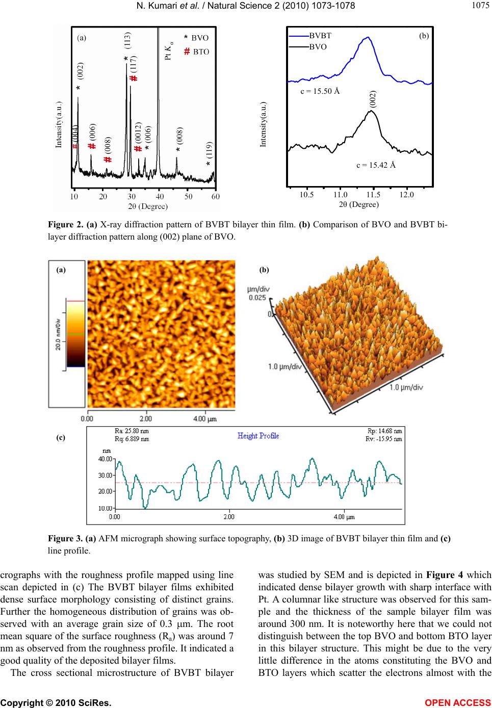 N. Kumari et al. / Natural Science 2 (2010) 1073-1078 Copyright © 2010 SciRes. OPEN ACCESS 107 1075 10.5 11.0 11.5 12.0 (b) Intensity (a.u.) (002) 2 (Degree) BVBT BVO 10.5 11.0 11.5 12.0 2θ (Degree) Intensity(a.u.) BVBT BVO (b) (002) c= 15.50Å c = 15.42 Å Figure 2. (a) X-ray diffraction pattern of BVBT bilayer thin film. (b) Comparison of BVO and BVBT bi- layer diffraction pattern along (002) plane of BVO. (b) (c) (a) Figure 3. (a) AFM micrograph showing surface topography, (b) 3D image of BVBT bilayer thin film and (c) line profile. crographs with the roughness profile mapped using line scan depicted in (c) The BVBT bilayer films exhibited dense surface morphology consisting of distinct grains. Further the homogeneous distribution of grains was ob- served with an average grain size of 0.3 m. The root mean square of the surface roughness (Ra) was around 7 nm as observed from the roughness profile. It indicated a good quality of the deposited bilayer films. The cross sectional microstructure of BVBT bilayer was studied by SEM and is depicted in Figure 4 which indicated dense bilayer growth with sharp interface with Pt. A columnar like structure was observed for this sam- ple and the thickness of the sample bilayer film was around 300 nm. It is noteworthy here that we could not distinguish between the top BVO and bottom BTO layer in this bilayer structure. This might be due to the very little difference in the atoms constituting the BVO and BTO layers which scatter the electrons almost with the 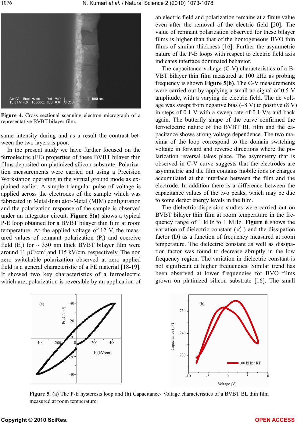 N. Kumari et al. / Natural Science 2 (2010) 1073-1078 Copyright © 2010 SciRes. OPEN ACCESS 1076 Figure 4. Cross sectional scanning electron micrograph of a representative BVBT bilayer film. same intensity during and as a result the contrast bet- ween the two layers is poor. In the present study we have further focused on the ferroelectric (FE) properties of these BVBT bilayer thin films deposited on platinized silicon substrate. Polariza- tion measurements were carried out using a Precision Workstation operating in the virtual ground mode as ex- plained earlier. A simple triangular pulse of voltage is applied across the electrodes of the sample which was fabricated in Metal-Insulator-Metal (MIM) configuration and the polarization response of the sample is observed under an integrator circuit. Figure 5(a) shows a typical P-E loop obtained for a BVBT bilayer thin film at room temperature. At the applied voltage of 12 V, the meas- ured values of remnant polarization (Pr) and coercive field (Ec) for ~ 350 nm thick BVBT bilayer film were around 11 C/cm2 and 115 kV/cm, respectively. The non zero switchable polarization observed at zero applied field is a general characteristic of a FE material [18-19]. It showed two key characteristics of a ferroelectric which are, polarization is reversible by an application of an electric field and polarization remains at a finite value even after the removal of the electric field [20]. The value of remnant polarization observed for these bilayer films is higher than that of the homogeneous BVO thin films of similar thickness [16]. Further the asymmetric nature of the P-E loops with respect to electric field axis indicates interface dominated behavior. The capacitance voltage (C-V) characteristics of a B- VBT bilayer thin film measured at 100 kHz as probing frequency is shown Figure 5(b). The C-V measurements were carried out by applying a small ac signal of 0.5 V amplitude, with a varying dc electric field. The dc volt- age was swept from negative bias (–8 V) to positive (8 V) in steps of 0.1 V with a sweep rate of 0.1 V/s and back again. The butterfly shape of the curve confirmed the ferroelectric nature of the BVBT BL film and the ca- pacitance shows strong voltage dependence. The two ma- xima of the loop correspond to the domain switching voltage in forward and reverse directions where the po- larization reversal takes place. The asymmetry that is observed in C-V curve suggests that the electrodes are asymmetric and the film contains mobile ions or charges accumulated at the interface between the film and the electrode. In addition there is a difference between the capacitance values of the two peaks, which may be due to some defect energy levels in the film. The dielectric dispersion studies were carried out on BVBT bilayer thin film at room temperature in the fre- quency range of 1 kHz to 1 MHz. Figure 6 shows the variation of dielectric constant (r ε) and the dissipation factor (D) as a function of frequency measured at room temperature. The dielectric constant as well as dissipa- tion factor was found to decrease abruptly in the low frequency region. The variation in dielectric constant is not significant at higher frequencies. Similar trend has been observed at lower frequencies for BVO films grown on platinized silicon substrate [16]. The small Figure 5. (a) The P-E hysteresis loop and (b) Capacitance- Voltage characteristics of a BVBT BL thin film measured at room temperature. 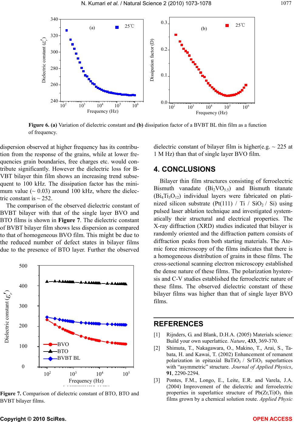 N. Kumari et al. / Natural Science 2 (2010) 1073-1078 Copyright © 2010 SciRes. OPEN ACCESS 107 1077 102103104105106 240 260 280 300 320 340 (a) Dielectric constant (r') Frequency (Hz) 25oC (a) 25℃ 10 2 10 3 10 4 10 5 10 6 Frequency (Hz) Dielectric constant () 340 320 300 280 260 240 102103104105106 0.0 0.1 0.2 0.3 (b) Fre q uenc y ( Hz ) Di ss i pa ti on f ac t or (D) 25oC 10 2 10 3 10 4 10 5 10 6 Frequency (Hz) Dissipation factor (D) 0.3 0.2 0.1 0.0 (b) 25℃ Figure 6. (a) Variation of dielectric constant and (b) dissipation factor of a BVBT BL thin film as a function of frequency. dispersion observed at higher frequency has its contribu- tion from the response of the grains, while at lower fre- quencies grain boundaries, free charges etc. would con- tribute significantly. However the dielectric loss for B- VBT bilayer thin film shows an increasing trend subse- quent to 100 kHz. The dissipation factor has the mini- mum value (~ 0.03) around 100 kHz, where the dielec- tric constant is ~ 252. The comparison of the observed dielectric constant of BVBT bilayer with that of the single layer BVO and BTO films is shown in Figure 7. The dielectric constant of BVBT bilayer film shows less dispersion as compared to that of homogeneous BVO film. This might be due to the reduced number of defect states in bilayer films due to the presence of BTO layer. Further the observed 102103104105 0 100 200 300 400 500 Dielectric constant(r') Frequency (Hz) BVO BTO BVBT BL BVO BTO BVBT BL 10 2 10 3 10 4 10 5 Frequency (Hz) 500 400 300 200 100 0 Dielectric constant () Figure 7. Comparison of dielectric constant of BTO, BTO and BVBT bilayer films. dielectric constant of bilayer film is higher(e.g. ~ 225 at 1 M Hz) than that of single layer BVO film. 4. CONCLUSIONS Bilayer thin film structures consisting of ferroelectric Bismuth vanadate (Bi2VO5.5) and Bismuth titanate (Bi4Ti3O12) individual layers were fabricated on plati- nized silicon substrate (Pt(111) / Ti / SiO2 / Si) using pulsed laser ablation technique and investigated system- atically their structural and electrical properties. The X-ray diffraction (XRD) studies indicated that bilayer is randomly oriented and the diffraction pattern consists of diffraction peaks from both starting materials. The Ato- mic force microscopy of the films indicates that there is a homogeneous distribution of grains in these films. The cross-sectional scanning electron microscopy established the dense nature of these films. The polarization hystere- sis and C-V studies established the ferroelectric nature of these films. The observed dielectric constant of these bilayer films was higher than that of single layer BVO films. REFERENCES [1] Rijnders, G. and Blank, D.H.A. (2005) Materials science: Build your own superlattice. Nature, 433, 369-370. [2] Shimuta, T., Nakagawara, O., Makino, T., Arai, S., Ta- bata, H. and Kawai, T. (2002) Enhancement of remanent polarization in epitaxial BaTiO3 / SrTiO3 superlattices with “asymmetric” structure. Journal of Applied Physics, 91, 2290-2294. [3] Pontes, F.M., Longo, E., Leite, E.R. and Varela, J.A. (2004) Improvement of the dielectric and ferroelectric properties in superlattice structure of Pb(Zr,Ti)O3 thin films grown by a chemical solution route. Applied Physic 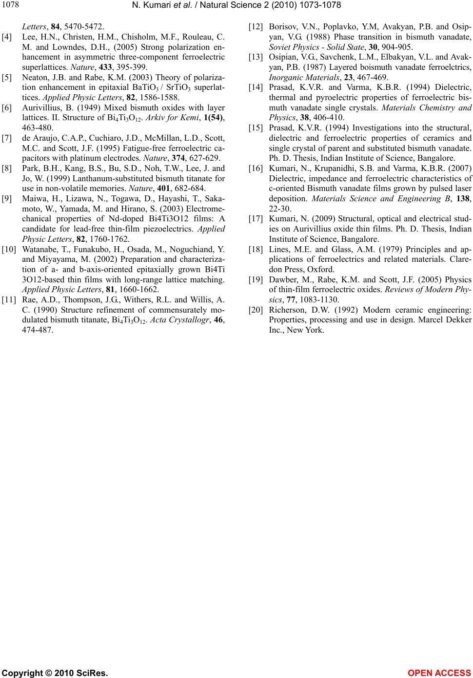 N. Kumari et al. / Natural Science 2 (2010) 1073-1078 Copyright © 2010 SciRes. OPEN ACCESS 1078 Letters, 84, 5470-5472. [4] Lee, H.N., Christen, H.M., Chisholm, M.F., Rouleau, C. M. and Lowndes, D.H., (2005) Strong polarization en- hancement in asymmetric three-component ferroelectric superlattices. Nature, 433, 395-399. [5] Neaton, J.B. and Rabe, K.M. (2003) Theory of polariza- tion enhancement in epitaxial BaTiO3 / SrTiO3 superlat- tices. Applied Physic Letters, 82, 1586-1588. [6] Aurivillius, B. (1949) Mixed bismuth oxides with layer lattices. II. Structure of Bi4Ti3O12. Arkiv for Kemi, 1(54), 463-480. [7] de Araujo, C.A.P., Cuchiaro, J.D., McMillan, L.D., Scott, M.C. and Scott, J.F. (1995) Fatigue-free ferroelectric ca- pacitors with platinum electrodes. Nature, 374, 627-629. [8] Park, B.H., Kang, B.S., Bu, S.D., Noh, T.W., Lee, J. and Jo, W. (1999) Lanthanum-substituted bismuth titanate for use in non-volatile memories. Nature, 401, 682-684. [9] Maiwa, H., Lizawa, N., Togawa, D., Hayashi, T., Saka- moto, W., Yamada, M. and Hirano, S. (2003) Electrome- chanical properties of Nd-doped Bi4Ti3O12 films: A candidate for lead-free thin-film piezoelectrics. Applied Physic Letters, 82, 1760-1762. [10] Watanabe, T., Funakubo, H., Osada, M., Noguchiand, Y. and Miyayama, M. (2002) Preparation and characteriza- tion of a- and b-axis-oriented epitaxially grown Bi4Ti 3O12-based thin films with long-range lattice matching. Applied Physic Letters, 81, 1660-1662. [11] Rae, A.D., Thompson, J.G., Withers, R.L. and Willis, A. C. (1990) Structure refinement of commensurately mo- dulated bismuth titanate, Bi4Ti3O12. Acta Crystallogr, 46, 474-487. [12] Borisov, V.N., Poplavko, Y.M, Avakyan, P.B. and Osip- yan, V.G. (1988) Phase transition in bismuth vanadate, Soviet Physics - Solid State, 30, 904-905. [13] Osipian, V.G., Savchenk, L.M., Elbakyan, V.L. and Avak- yan, P.B. (1987) Layered boismuth vanadate ferroelctrics, Inorganic Materials, 23, 467-469. [14] Prasad, K.V.R. and Varma, K.B.R. (1994) Dielectric, thermal and pyroelectric properties of ferroelectric bis- muth vanadate single crystals. Materials Chemistry and Physics, 38, 406-410. [15] Prasad, K.V.R. (1994) Investigations into the structural, dielectric and ferroelectric properties of ceramics and single crystal of parent and substituted bismuth vanadate. Ph. D. Thesis, Indian Institute of Science, Bangalore. [16] Kumari, N., Krupanidhi, S.B. and Varma, K.B.R. (2007) Dielectric, impedance and ferroelectric characteristics of c-oriented Bismuth vanadate films grown by pulsed laser deposition. Materials Science and Engineering B, 138, 22-30. [17] Kumari, N. (2009) Structural, optical and electrical stud- ies on Aurivillius oxide thin films. Ph. D. Thesis, Indian Institute of Science, Bangalore. [18] Lines, M.E. and Glass, A.M. (1979) Principles and ap- plications of ferroelectrics and related materials. Clare- don Press, Oxford. [19] Dawber, M., Rabe, K.M. and Scott, J.F. (2005) Physics of thin-film ferroelectric oxides. Reviews of Modern Phy- sics, 77, 1083-1130. [20] Richerson, D.W. (1992) Modern ceramic engineering: Properties, processing and use in design. Marcel Dekker Inc., New York. |