

Paper Menu >>
Journal Menu >>
 Journal of Surface Engineered Materials and Advanced Technology, 2013, 3, 84-88 http://dx.doi.org/10.4236/jsemat.2013.31A012 Published Online February 2013 (http://www.scirp.org/journal/jsemat) Film-Forming Properties of Fullerene Derivatives in Electrospray Deposition Method Kazumasa Takeshi1,2, Kenji Takagi1,2, Takeshi Fukuda1,2, Teiji Chihara1, Yusuke Tajima1,2* 1Department of Functional Materials Science, Graduate School of Science and Engineering, Saitama University, Saitama, Japan; 2RIKEN, Saitama, Japan. Email: *[email protected] Received November 27th, 2012; revised December 28th, 2012; accepted January 4th, 2013 ABSTRACT Thin films of three types of fullerene derivatives were prepared through the electrospray deposition (ESD) method. The optimized conditions for the fabrication of the thin films were investigated for different types of fullerene derivatives: [6,6]-phenyl-C61-butyric acid methyl ester, [6,6]-phenyl-C71-butyric acid methyl ester, and indene-C60-monoadduct. The spray diameter during the ESD process was observed as a function of the supply rate achieved by changing the applied voltage. In all cases, the spray diameter increased with increasing applied voltage, reaching the maximum diameter (Dmax) in the voltage range 4 to 6 kV. It was clear that Dmax was influenced by the dipole moments of the fullerene de- rivatives (as calculated by density functional theory methods). Scanning electron microscopy observation of the fabri- cated thin films showed that imbricated structures were formed through the stacking of the fullerene-derivative sheets. Atomic force microscopy images revealed that the density of the imbricated structure was dependent on the spray di- ameter during the ESD process, and the root-mean-square roughness of the film surface decreased with increasing ap- plied voltage. These findings suggest that the ESD method will be effective for the preparation of fullerene-derivative thin films for the production of organic devices. Keywords: Electrospray Deposition Method; Fullerene Derivative; Thin Film; Scanning Electron Microscope; Imbricated Structure; Atomic Force Microscope; Root-Mean-Square Roughness 1. Introduction Organic devices are of interest owing to their special advantages over inorganic semiconductor devices, such as their light weight, flexibility, large device area, low- cost manufacture, and the applicability of solution-proc- essing techniques. Solution processes have already been demonstrated with organic semiconductors for the fabric- cation of light-emitting diodes [1], thin-film transistors [2], and photovoltaic cells [3]. On the contrary, a bilayer heterojunction photovoltaic system [4-6], in which donor and acceptor films are stacked sequentially on top of one another, is difficult to form practically with different or- ganic compounds using normal solution processes such as spin-coating, dip-coating, screen printing, and inkjet printing. This is because these solution processes cause the dissolution of the underlying organic layer while coating the upper organic layer. In addition, the forma- tion of a single layer of fullerene or a fullerene derivative through a solution process has innate drawbacks: the thickness and surface roughness cannot be controlled because of the poor film-forming ability due to strong cohesive forces, and these species have low solubility in common organic solvents. Therefore, the considerable amount of research on the fabrication of fullerene films has dealt almost exclusively with as-deposited films, consisting of vacuum-sublimed C60 on top of a spin- coated polymer film [4-6]. However, most fullerene de- rivatives cannot be deposited by vacuum processes, and there have been few reports on the fabrication of ful- lerene-derivative films by the spin-coating process [7]. For the fabrication of fullerene-derivative-based bilayer heterojunction photovoltaic devices, an appropriate solu- tion process for fullerene-derivative thin-film deposition is desirable. Recently, our research group has investigated a new electrospray deposition (ESD) method as a film-forma- tion process for organic semiconductors, which can be adapted for the fabrication of organic photovoltaic (OPV) devices with regioregular poly(3-hexylthiophene-2,5-diyl) and fullerene derivatives [8]. In this ESD process, a high voltage of several kilovolts is applied to the organic solu- tion, which is then divided into innumerable droplets with diameters of a few micrometers [9]. As a result, following solvent evaporation, organic semiconductor *Corresponding author. Copyright © 2013 SciRes. JSEMAT 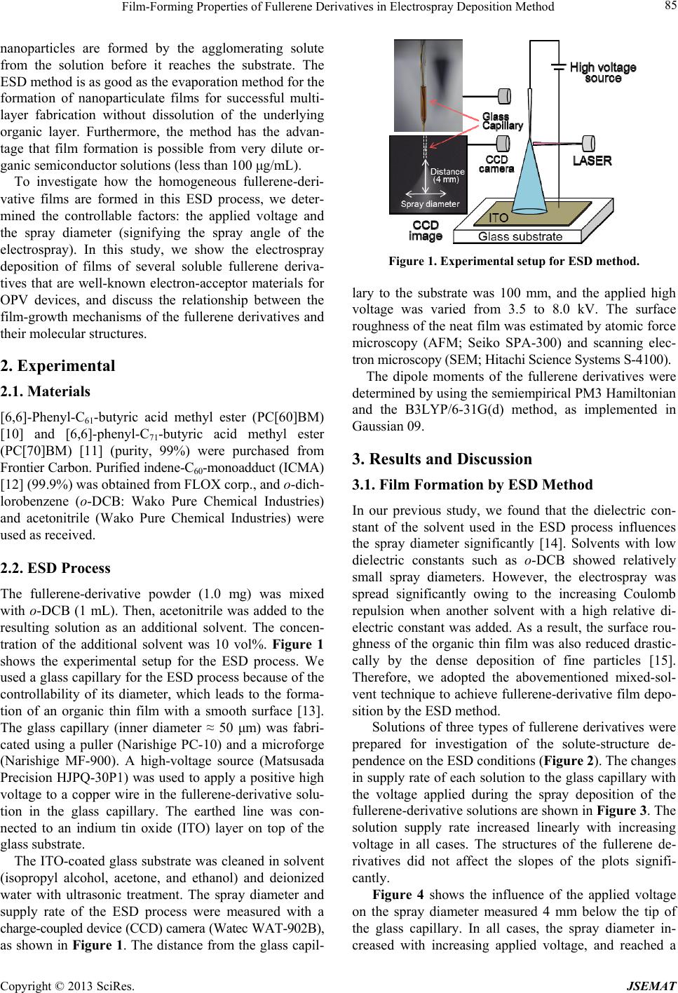 Film-Forming Properties of Fullerene Derivatives in Electrospray Deposition Method 85 nanoparticles are formed by the agglomerating solute from the solution before it reaches the substrate. The ESD method is as good as the evaporation method for the formation of nanoparticulate films for successful multi- layer fabrication without dissolution of the underlying organic layer. Furthermore, the method has the advan- tage that film formation is possible from very dilute or- ganic semiconductor solutions (less than 100 μg/mL). To investigate how the homogeneous fullerene-deri- vative films are formed in this ESD process, we deter- mined the controllable factors: the applied voltage and the spray diameter (signifying the spray angle of the electrospray). In this study, we show the electrospray deposition of films of several soluble fullerene deriva- tives that are well-known electron-acceptor materials for OPV devices, and discuss the relationship between the film-growth mechanisms of the fullerene derivatives and their molecular structures. 2. Experimental 2.1. Materials [6,6]-Phenyl-C61-butyric acid methyl ester (PC[60]BM) [10] and [6,6]-phenyl-C71-butyric acid methyl ester (PC[70]BM) [11] (purity, 99%) were purchased from Frontier Carbon. Purified indene-C60-monoadduct (ICMA) [12] (99.9%) was obtained from FLOX corp., and o-dich- lorobenzene (o-DCB: Wako Pure Chemical Industries) and acetonitrile (Wako Pure Chemical Industries) were used as received. 2.2. ESD Process The fullerene-derivative powder (1.0 mg) was mixed with o-DCB (1 mL). Then, acetonitrile was added to the resulting solution as an additional solvent. The concen- tration of the additional solvent was 10 vol%. Figure 1 shows the experimental setup for the ESD process. We used a glass capillary for the ESD process because of the controllability of its diameter, which leads to the forma- tion of an organic thin film with a smooth surface [13]. The glass capillary (inner diameter ≈ 50 μm) was fabri- cated using a puller (Narishige PC-10) and a microforge (Narishige MF-900). A high-voltage source (Matsusada Precision HJPQ-30P1) was used to apply a positive high voltage to a copper wire in the fullerene-derivative solu- tion in the glass capillary. The earthed line was con- nected to an indium tin oxide (ITO) layer on top of the glass substrate. The ITO-coated glass substrate was cleaned in solvent (isopropyl alcohol, acetone, and ethanol) and deionized water with ultrasonic treatment. The spray diameter and supply rate of the ESD process were measured with a charge-coupled device (CCD) camera (Watec WAT-902B), as shown in Figure 1. The distance from the glass capil- Figure 1. Experimental setup for ESD method. lary to the substrate was 100 mm, and the applied high voltage was varied from 3.5 to 8.0 kV. The surface roughness of the neat film was estimated by atomic force microscopy (AFM; Seiko SPA-300) and scanning elec- tron microscopy (SEM; Hitachi Science Systems S-4100). The dipole moments of the fullerene derivatives were determined by using the semiempirical PM3 Hamiltonian and the B3LYP/6-31G(d) method, as implemented in Gaussian 09. 3. Results and Discussion 3.1. Film Formation by ESD Method In our previous study, we found that the dielectric con- stant of the solvent used in the ESD process influences the spray diameter significantly [14]. Solvents with low dielectric constants such as o-DCB showed relatively small spray diameters. However, the electrospray was spread significantly owing to the increasing Coulomb repulsion when another solvent with a high relative di- electric constant was added. As a result, the surface rou- ghness of the organic thin film was also reduced drastic- cally by the dense deposition of fine particles [15]. Therefore, we adopted the abovementioned mixed-sol- vent technique to achieve fullerene-derivative film depo- sition by the ESD method. Solutions of three types of fullerene derivatives were prepared for investigation of the solute-structure de- pendence on the ESD conditions (Figure 2). The changes in supply rate of each solution to the glass capillary with the voltage applied during the spray deposition of the fullerene-derivative solutions are shown in Figure 3. The solution supply rate increased linearly with increasing voltage in all cases. The structures of the fullerene de- rivatives did not affect the slopes of the plots signifi- cantly. Figure 4 shows the influence of the applied voltage on the spray diameter measured 4 mm below the tip of the glass capillary. In all cases, the spray diameter in- creased with increasing applied voltage, and reached a Copyright © 2013 SciRes. JSEMAT 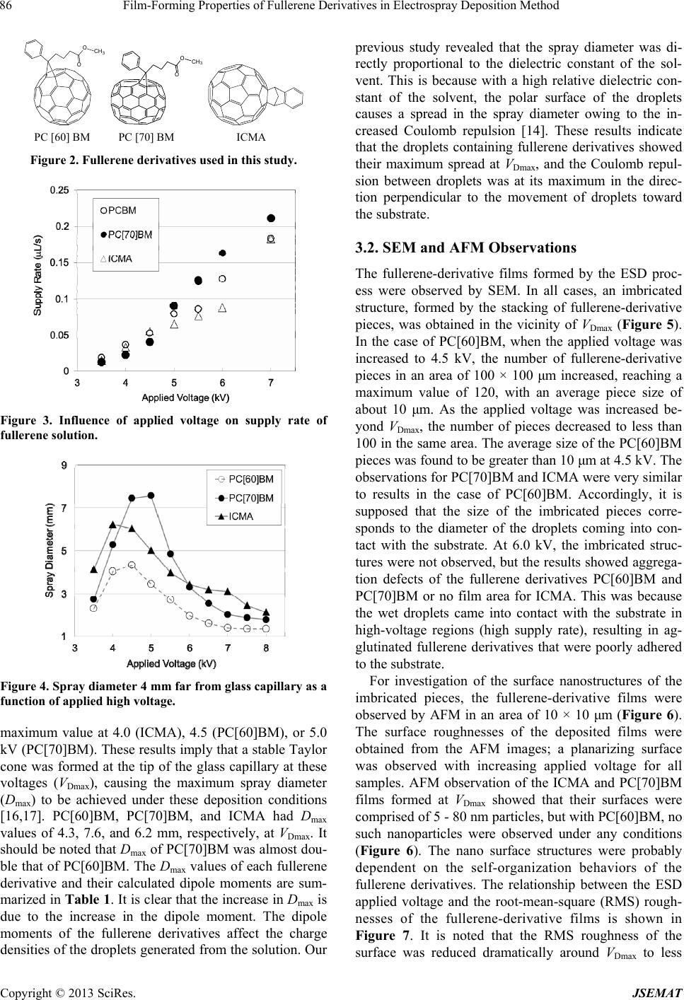 Film-Forming Properties of Fullerene Derivatives in Electrospray Deposition Method 86 O O CH 3 O O CH 3 PC [60] BM PC [70] BM ICMA Figure 2. Fullerene derivatives used in this study. Figure 3. Influence of applied voltage on supply rate of fullerene solution. Figure 4. Spray diameter 4 mm far from glass capillary as a function of applied high voltage. maximum value at 4.0 (ICMA), 4.5 (PC[60]BM), or 5.0 kV (PC[70]BM). These results imply that a stable Taylor cone was formed at the tip of the glass capillary at these voltages (VDmax), causing the maximum spray diameter (Dmax) to be achieved under these deposition conditions [16,17]. PC[60]BM, PC[70]BM, and ICMA had Dmax values of 4.3, 7.6, and 6.2 mm, respectively, at VDmax. It should be noted that Dmax of PC[70]BM was almost dou- ble that of PC[60]BM. The Dmax values of each fullerene derivative and their calculated dipole moments are sum- marized in Table 1 . It is clear that the increase in Dmax is due to the increase in the dipole moment. The dipole moments of the fullerene derivatives affect the charge densities of the droplets generated from the solution. Our previous study revealed that the spray diameter was di- rectly proportional to the dielectric constant of the sol- vent. This is because with a high relative dielectric con- stant of the solvent, the polar surface of the droplets causes a spread in the spray diameter owing to the in- creased Coulomb repulsion [14]. These results indicate that the droplets containing fullerene derivatives showed their maximum spread at VDmax, and the Coulomb repul- sion between droplets was at its maximum in the direc- tion perpendicular to the movement of droplets toward the substrate. 3.2. SEM and AFM Observations The fullerene-derivative films formed by the ESD proc- ess were observed by SEM. In all cases, an imbricated structure, formed by the stacking of fullerene-derivative pieces, was obtained in the vicinity of VDmax (Figure 5). In the case of PC[60]BM, when the applied voltage was increased to 4.5 kV, the number of fullerene-derivative pieces in an area of 100 × 100 μm increased, reaching a maximum value of 120, with an average piece size of about 10 μm. As the applied voltage was increased be- yond VDmax, the number of pieces decreased to less than 100 in the same area. The average size of the PC[60]BM pieces was found to be greater than 10 μm at 4.5 kV. The observations for PC[70]BM and ICMA were very similar to results in the case of PC[60]BM. Accordingly, it is supposed that the size of the imbricated pieces corre- sponds to the diameter of the droplets coming into con- tact with the substrate. At 6.0 kV, the imbricated struc- tures were not observed, but the results showed aggrega- tion defects of the fullerene derivatives PC[60]BM and PC[70]BM or no film area for ICMA. This was because the wet droplets came into contact with the substrate in high-voltage regions (high supply rate), resulting in ag- glutinated fullerene derivatives that were poorly adhered to the substrate. For investigation of the surface nanostructures of the imbricated pieces, the fullerene-derivative films were observed by AFM in an area of 10 × 10 μm (Figure 6). The surface roughnesses of the deposited films were obtained from the AFM images; a planarizing surface was observed with increasing applied voltage for all samples. AFM observation of the ICMA and PC[70]BM films formed at VDmax showed that their surfaces were comprised of 5 - 80 nm particles, but with PC[60]BM, no such nanoparticles were observed under any conditions (Figure 6). The nano surface structures were probably dependent on the self-organization behaviors of the fullerene derivatives. The relationship between the ESD applied voltage and the root-mean-square (RMS) rough- nesses of the fullerene-derivative films is shown in Figure 7. It is noted that the RMS roughness of the surface was reduced dramatically around VDmax to less Copyright © 2013 SciRes. JSEMAT 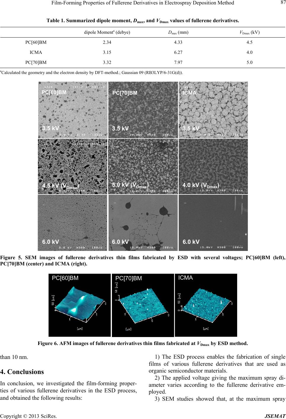 Film-Forming Properties of Fullerene Derivatives in Electrospray Deposition Method Copyright © 2013 SciRes. JSEMAT 87 Table 1. Summarized dipole moment, Dmax, and VDmax values of fullerene derivatives. dipole Momenta (debye) Dmax (mm) VDmax (kV) PC[60]BM 2.34 4.33 4.5 ICMA 3.15 6.27 4.0 PC[70]BM 3.32 7.97 5.0 aCalculated the geometry and the electron density by DFT-method.; Gaussian 09 (RB3LYP/6-31G(d)). 3.5 kV 4.5 kV (VDmax) 6.0 kV6.0 kV6.0 kV 5.0 kV(VDmax)4.0 k V(VDmax) 3.5 kV3.5 kV PC[60]BM PC[70]BM ICMA Figure 5. SEM images of fullerene derivatives thin films fabricated by ESD with several voltages; PC[60]BM (left), PC[70]BM (center) and ICMA (right). PC[60]BM PC[70]BM IC MA Figure 6. AFM images of fullerene derivatives thin films fabricated at VDmax by ESD method. 1) The ESD process enables the fabrication of single films of various fullerene derivatives that are used as organic semiconductor materials. than 10 nm. 4. Conclusions 2) The applied voltage giving the maximum spray di- ameter varies according to the fullerene derivative em- ployed. In conclusion, we investigated the film-forming proper- ties of various fullerene derivatives in the ESD process, and obtained the following results: 3) SEM studies showed that, at the maximum spray 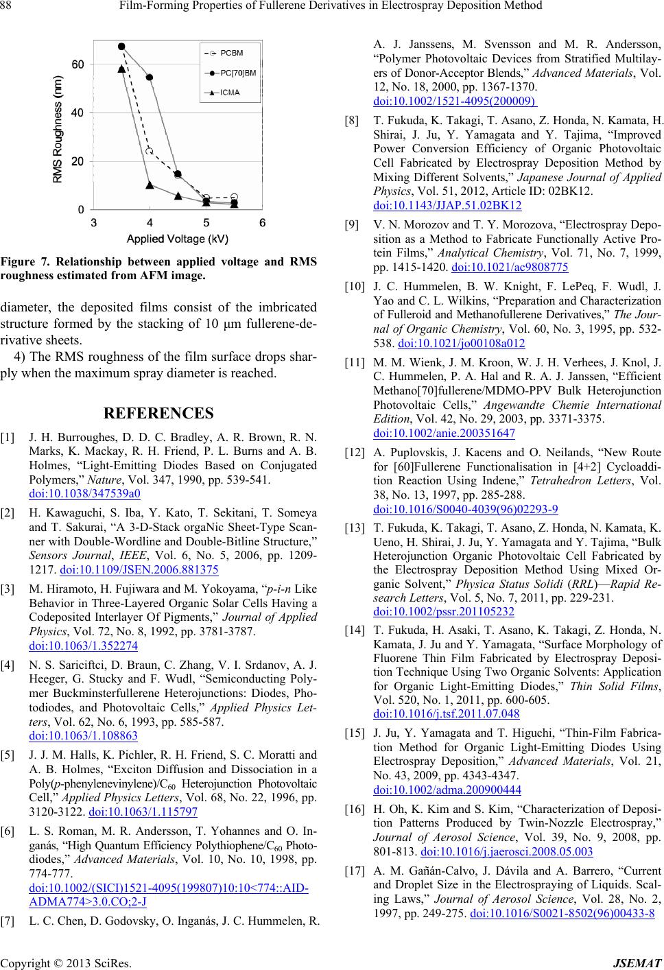 Film-Forming Properties of Fullerene Derivatives in Electrospray Deposition Method 88 Figure 7. Relationship between applied voltage and RMS roughness estimated from AFM image. diameter, the deposited films consist of the imbricated structure formed by the stacking of 10 μm fullerene-de- rivative sheets. 4) The RMS roughness of the film surface drops shar- ply when the maximum spray diameter is reached. REFERENCES [1] J. H. Burroughes, D. D. C. Bradley, A. R. Brown, R. N. Marks, K. Mackay, R. H. Friend, P. L. Burns and A. B. Holmes, “Light-Emitting Diodes Based on Conjugated Polymers,” Nature, Vol. 347, 1990, pp. 539-541. doi:10.1038/347539a0 [2] H. Kawaguchi, S. Iba, Y. Kato, T. Sekitani, T. Someya and T. Sakurai, “A 3-D-Stack orgaNic Sheet-Type Scan- ner with Double-Wordline and Double-Bitline Structure,” Sensors Journal, IEEE, Vol. 6, No. 5, 2006, pp. 1209- 1217. doi:10.1109/JSEN.2006.881375 [3] M. Hiramoto, H. Fujiwara and M. Yokoyama, “p-i-n Like Behavior in Three-Layered Organic Solar Cells Having a Codeposited Interlayer Of Pigments,” Journal of Applied Physics, Vol. 72, No. 8, 1992, pp. 3781-3787. doi:10.1063/1.352274 [4] N. S. Sariciftci, D. Braun, C. Zhang, V. I. Srdanov, A. J. Heeger, G. Stucky and F. Wudl, “Semiconducting Poly- mer Buckminsterfullerene Heterojunctions: Diodes, Pho- todiodes, and Photovoltaic Cells,” Applied Physics Let- ters, Vol. 62, No. 6, 1993, pp. 585-587. doi:10.1063/1.108863 [5] J. J. M. Halls, K. Pichler, R. H. Friend, S. C. Moratti and A. B. Holmes, “Exciton Diffusion and Dissociation in a Poly(p-phenylenevinylene)/C60 Heterojunction Photovoltaic Cell,” Applied Physics Letters, Vol. 68, No. 22, 1996, pp. 3120-3122. doi:10.1063/1.115797 [6] L. S. Roman, M. R. Andersson, T. Yohannes and O. In- ganás, “High Quantum Efficiency Polythiophene/C60 Photo- diodes,” Advanced Materials, Vol. 10, No. 10, 1998, pp. 774-777. doi:10.1002/(SICI)1521-4095(199807)10:10<774::AID- ADMA774>3.0.CO;2-J [7] L. C. Chen, D. Godovsky, O. Inganás, J. C. Hummelen, R. A. J. Janssens, M. Svensson and M. R. Andersson, “Polymer Photovoltaic Devices from Stratified Multilay- ers of Donor-Acceptor Blends,” Advanced Materials, Vol. 12, No. 18, 2000, pp. 1367-1370. doi:10.1002/1521-4095(200009) [8] T. Fukuda, K. Takagi, T. Asano, Z. Honda, N. Kamata, H. Shirai, J. Ju, Y. Yamagata and Y. Tajima, “Improved Power Conversion Efficiency of Organic Photovoltaic Cell Fabricated by Electrospray Deposition Method by Mixing Different Solvents,” Japanese Journal of Applied Physics, Vol. 51, 2012, Article ID: 02BK12. doi:10.1143/JJAP.51.02BK12 [9] V. N. Morozov and T. Y. Morozova, “Electrospray Depo- sition as a Method to Fabricate Functionally Active Pro- tein Films,” Analytical Chemistry, Vol. 71, No. 7, 1999, pp. 1415-1420. doi:10.1021/ac9808775 [10] J. C. Hummelen, B. W. Knight, F. LePeq, F. Wudl, J. Yao and C. L. Wilkins, “Preparation and Characterization of Fulleroid and Methanofullerene Derivatives,” The Jour- nal of Organic Chemistry, Vol. 60, No. 3, 1995, pp. 532- 538. doi:10.1021/jo00108a012 [11] M. M. Wienk, J. M. Kroon, W. J. H. Verhees, J. Knol, J. C. Hummelen, P. A. Hal and R. A. J. Janssen, “Efficient Methano[70]fullerene/MDMO-PPV Bulk Heterojunction Photovoltaic Cells,” Angewandte Chemie International Edition, Vol. 42, No. 29, 2003, pp. 3371-3375. doi:10.1002/anie.200351647 [12] A. Puplovskis, J. Kacens and O. Neilands, “New Route for [60]Fullerene Functionalisation in [4+2] Cycloaddi- tion Reaction Using Indene,” Tetrahedron Letters, Vol. 38, No. 13, 1997, pp. 285-288. doi:10.1016/S0040-4039(96)02293-9 [13] T. Fukuda, K. Takagi, T. Asano, Z. Honda, N. Kamata, K. Ueno, H. Shirai, J. Ju, Y. Yamagata and Y. Tajima, “Bulk Heterojunction Organic Photovoltaic Cell Fabricated by the Electrospray Deposition Method Using Mixed Or- ganic Solvent,” Physica Status Solidi (RRL)—Rapid Re- search Letters, Vol. 5, No. 7, 2011, pp. 229-231. doi:10.1002/pssr.201105232 [14] T. Fukuda, H. Asaki, T. Asano, K. Takagi, Z. Honda, N. Kamata, J. Ju and Y. Yamagata, “Surface Morphology of Fluorene Thin Film Fabricated by Electrospray Deposi- tion Technique Using Two Organic Solvents: Application for Organic Light-Emitting Diodes,” Thin Solid Films, Vol. 520, No. 1, 2011, pp. 600-605. doi:10.1016/j.tsf.2011.07.048 [15] J. Ju, Y. Yamagata and T. Higuchi, “Thin-Film Fabrica- tion Method for Organic Light-Emitting Diodes Using Electrospray Deposition,” Advanced Materials, Vol. 21, No. 43, 2009, pp. 4343-4347. doi:10.1002/adma.200900444 [16] H. Oh, K. Kim and S. Kim, “Characterization of Deposi- tion Patterns Produced by Twin-Nozzle Electrospray,” Journal of Aerosol Science, Vol. 39, No. 9, 2008, pp. 801-813. doi:10.1016/j.jaerosci.2008.05.003 [17] A. M. Gañán-Calvo, J. Dávila and A. Barrero, “Current and Droplet Size in the Electrospraying of Liquids. Scal- ing Laws,” Journal of Aerosol Science, Vol. 28, No. 2, 1997, pp. 249-275. doi:10.1016/S0021-8502(96)00433-8 Copyright © 2013 SciRes. JSEMAT |