

Paper Menu >>
Journal Menu >>
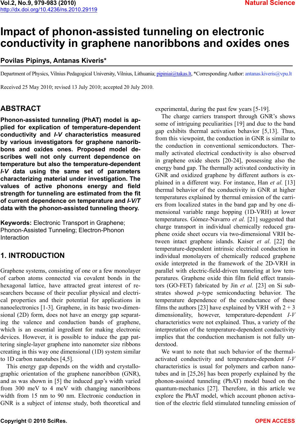 Vol.2, No.9, 979-983 (2010) Natural Science http://dx.doi.org/10.4236/ns.2010.29119 Copyright © 2010 SciRes. OPEN ACCESS Impact of phonon-assisted tunneling on electronic conductivity in graphene nanoribbons and oxides ones Povilas Pipinys, Antanas Kiveris* Department of Physics, Vilnius Pedagogical University, Vilnius, Lithuania; [email protected], *Corresponding Author: [email protected] Received 25 May 2010; revised 13 July 2010; accepted 20 July 2010. ABSTRACT Phonon-assisted tunneling (PhAT) model is ap- plied for explication of temperature-dependent conductivity and I-V characteristics measured by various investigators for graphene nanorib- bons and oxides ones. Proposed model de- scribes well not only current dependence on temperature but also the temperature-dependent I-V data using the same set of parameters characterizing material under investigation. The values of active phonons energy and field strength for tunneling are estimated from the fit of current dependence on temperature and I-V/T data with the phonon-assisted tunneling theory. Keywords: Electronic Transport in Graphene; Phonon-Assisted Tunneling; Electron-Phonon Interaction 1. INTRODUCTION Graphene systems, consisting of one or a few monolayer of carbon atoms connected via covalent bonds in the hexagonal lattice, have attracted great interest of re- searchers because of their peculiar physical and electri- cal properties and their potential for applications in nanoelectronics [1-3]. Graphene, in its basic two-dimen- sional (2D) form, does not have an energy gap separat- ing the valence and conduction bands of graphene, which is an essential ingredient for making electronic devices. However, it is possible to induce the gap pat- tering single-layer graphene into nanometer size ribbons creating in this way one dimensional (1D) system similar to 1D carbon nanotubes [4,5]. This energy gap depends on the width and crystallo- graphic orientation of the graphene nanoribbon (GNR), and as was shown in [5] the induced gap’s width varied from 300 meV to 4 meV with changing nanoribbons width from 15 nm to 90 nm. Electronic conduction in GNR is a subject of intense study, both theoretical and experimental, during the past few years [5-19]. The charge carriers transport through GNR’s shows some of intriguing peculiarities [19] and due to the band gap exhibits thermal activation behavior [5,13]. Thus, from this viewpoint, the conduction in GNR is similar to the conduction in conventional semiconductors. Ther- mally activated electrical conductivity is also observed in graphene oxide sheets [20-24], possessing also the energy band gap. The thermally activated conductivity in GNR and oxidized graphene by different authors is ex- plained in a different way. For instance, Han et al. [13] thermal behavior of the conductivity in GNR at higher temperatures explained by thermal emission of the carri- ers from localized states in the band gap and by one di- mensional variable range hopping (1D-VRH) at lower temperatures. Gómez-Navarro et al. [21] suggested that charge transport in individual chemically reduced gra- phene oxide sheet occurs via two-dimensional VRH be- tween intact graphene islands. Kaiser et al. [22] the temperature-dependent intrinsic electrical conduction in individual monolayers of chemically reduced graphene oxide interpreted in the framework of the 2D-VRH in parallel with electric-field-driven tunneling at low tem- peratures. Graphene oxide thin film field effect transis- tors (GO-FET) fabricated by Jin et al. [23] on Si sub- strates showed p-type semiconducting behavior. The temperature dependence of the conductance of these films the authors [23] have explained by VRH with 2 + 3 dimensionality, however, temperature-dependent I-V characteristics were not explained. Thus, a variety of the interpretation of the temperature-dependent conductivity implies that the conduction mechanism is not fully un- derstood. We want to note that such behavior of the thermal- activated conductivity and temperature-dependent I-V characteristics is usual for polymers and carbon nano- tubes and in [25,26] has been properly explained by the phonon-assisted tunneling (PhAT) model based on the quantum-mechanics [27]. Therefore, in this article we explore the PhAT model, which account phonon activa- tion of the electric field stimulated tunneling emission of 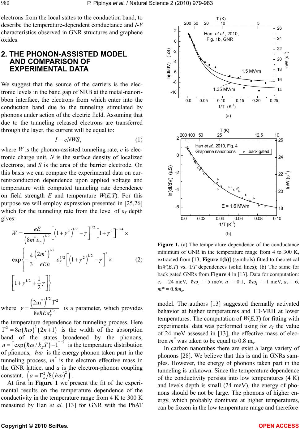 P. Pipinys et al. / Natural Science 2 (2010) 979-983 Copyright © 2010 SciRes. OPEN ACCESS 980 electrons from the local states to the conduction band, to describe the temperature-dependent conductance and I-V characteristics observed in GNR structures and graphene oxides. 2. THE PHONON-ASSISTED MODEL AND COMPARISON OF EXPERIMENTAL DATA We suggest that the source of the carriers is the elec- tronic levels in the band gap of NRB at the metal-nanori- bbon interface, the electrons from which enter into the conduction band due to the tunneling stimulated by phonons under action of the electric field. Assuming that due to the tunneling released electrons are transferred through the layer, the current will be equal to: ,I=eNWS (1) where W is the phonon-assisted tunneling rate, e is elec- tronic charge unit, N is the surface density of localized electrons, and S is the area of the barrier electrode. On this basis we can compare the experimental data on cur- rent/conduction dependence upon applied voltage and temperature with computed tunneling rate dependence on field strength E and temperature W(E,T). For this purpose we will employ expression presented in [25,26] which for the tunneling rate from the level of εT depth gives: 1/2 1/21/4 22 1/2 * 1/2 *2 1/2 3/2 2 1/2 11 8 2 4 exp 1 3 1 12 T T eE W m m eE (2) where 1/2 *2 1/2 2m 8T eE is a parameter, which provides the temperature dependence for tunneling process. Here 2 2821an is the width of the absorption band of the states broadened by the phonons, 1 exp /1 B nkT is the temperature distribution of phonons, is the energy phonon taken part in the tunneling process, m* is the electron effective mass in the GNR lattice, and a is the electron-phonon coupling constant, 2 28 o a . At first in Figure 1 we present the fit of the experi- mental results on the temperature dependence of the conductivity in the temperature range from 4 K to 300 K measured by Han et al. [13] for GNR with the PhAT -10 -8 -6 -4 -2 0 2 14 16 18 20 22 24 26 1.5 MV/m ln(dI/dV) (S) 1/T ( K-1 ) Han et al., 2010, Fig. 1b, GNR 1.35 MV/m () 0.0 0.05 0.10 0.15 0.20 0.25 T (K) lnW (s-1) 200 50 20 10 5 (a) -6 -4 -2 0 2 18 20 22 24 26 ln(dI/dV) (S) 1/T ( K-1 ) back gated Han et al. , 2010, Fig. 4 Graphene nanoribons E = 1.6 MV/m 0.0 0.02 0.04 0.06 0.08 0.10 lnW (s-1) 200 100 50 25 12.5 10 T (K) (b) Figure 1. (a) The temperature dependence of the conductance minimum of GNR in the temperature range from 4 to 300 K, extracted from [13, Figure 1(b)] (symbols) fitted to theoretical lnW(E,T) vs. 1/T dependences (solid lines); (b) The same for back gated GNRs from Figure 4 in [13]. Data for computation: εT = 24 meV, 1 = 5 meV, a1 = 0.1, 2 = 1 meV, a2 = 6, m* = 0.8me. model. The authors [13] suggested thermally activated behavior at higher temperatures and 1D-VRH at lower temperatures. The computation of W(E,T) for fitting with experimental data was performed using for εT the value of 24 meV assessed in [13], the effective mass of elec- tron m* was taken to be equal to 0.8 me. In carbon nanotubes there are exist a large variety of phonons [28]. We believe that this is and in GNRs sam- ples. However, the energy of phonons taken part in the tunneling is unknown. Since the temperature dependence of the conductivity persists into low temperatures (4 K) and levels depth is small (24 meV), the energy of pho- nons should be not be large. The phonons of higher en- ergy, which probably dominate at higher temperatures, can be frozen in the low temperature range and therefore 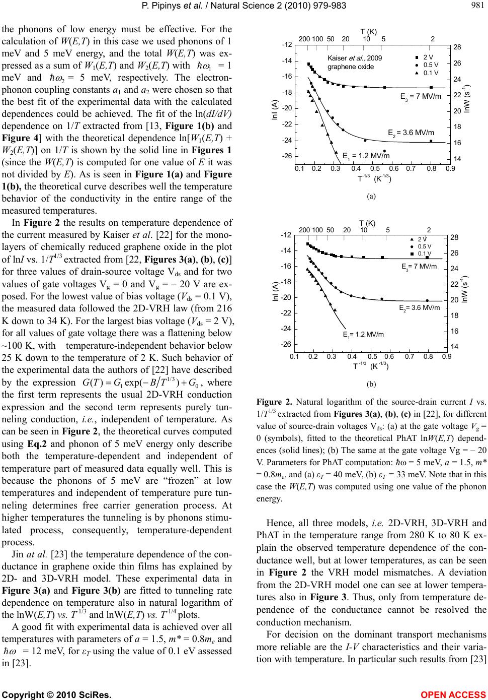 P. Pipinys et al. / Natural Science 2 (2010) 979-983 Copyright © 2010 SciRes. OPEN ACCESS 981 981 the phonons of low energy must be effective. For the calculation of W(E,T) in this case we used phonons of 1 meV and 5 meV energy, and the total W(E,T) was ex- pressed as a sum of W1(E,T) and W2(E,T) with 1 = 1 meV and 2 = 5 meV, respectively. The electron- phonon coupling constants a1 and a2 were chosen so that the best fit of the experimental data with the calculated dependences could be achieved. The fit of the ln(dI/dV) dependence on 1/T extracted from [13, Figure 1(b) and Figure 4] with the theoretical dependence ln[W1(E,T) + W2(E,T)] on 1/T is shown by the solid line in Figures 1 (since the W(E,T) is computed for one value of E it was not divided by E). As is seen in Figure 1(a) and Figure 1(b), the theoretical curve describes well the temperature behavior of the conductivity in the entire range of the measured temperatures. In Figure 2 the results on temperature dependence of the current measured by Kaiser et al. [22] for the mono- layers of chemically reduced graphene oxide in the plot of lnI vs. 1/T1/3 extracted from [22, Figures 3(a), (b), (c)] for three values of drain-source voltage Vds and for two values of gate voltages Vg = 0 and Vg = – 20 V are ex- posed. For the lowest value of bias voltage (Vds = 0.1 V), the measured data followed the 2D-VRH law (from 216 K down to 34 K). For the largest bias voltage (Vds = 2 V), for all values of gate voltage there was a flattening below ~100 K, with temperature-independent behavior below 25 K down to the temperature of 2 K. Such behavior of the experimental data the authors of [22] have described by the expression 1/3 10 () exp()GT GBTG, where the first term represents the usual 2D-VRH conduction expression and the second term represents purely tun- neling conduction, i.e., independent of temperature. As can be seen in Figure 2, the theoretical curves computed using Eq.2 and phonon of 5 meV energy only describe both the temperature-dependent and independent of temperature part of measured data equally well. This is because the phonons of 5 meV are “frozen” at low temperatures and independent of temperature pure tun- neling determines free carrier generation process. At higher temperatures the tunneling is by phonons stimu- lated process, consequently, temperature-dependent process. Jin at al. [23] the temperature dependence of the con- ductance in graphene oxide thin films has explained by 2D- and 3D-VRH model. These experimental data in Figure 3(a) and Figure 3(b) are fitted to tunneling rate dependence on temperature also in natural logarithm of the lnW(E,T) vs. T-1/3 and lnW(E,T) vs. T-1/4 plots. A good fit with experimental data is achieved over all temperatures with parameters of a = 1.5, m* = 0.8me and = 12 meV, for εT using the value of 0.1 eV assessed in [23]. -26 -24 -22 -20 -18 -16 -14 -12 14 16 18 20 22 24 26 28 E1 = 1.2 MV/m E2 = 3.6 MV/m lnI (A) T-1/3 (K-1/3) 2 V 0.5 V 0.1 V Kaiser et al. , 2009 graphene oxide E3 = 7 MV/m 0.1 0.2 0.3 0.4 0.5 0.6 0.7 0.8 0.9 lnW (s-1) 200 100 50 20 10 5 2 T (K) (a) -26 -24 -22 -20 -18 -16 -14 -12 14 16 18 20 22 24 26 28 lnI (A) T -1/3 (K -1/3) 2 V 0.5 V 0.1 V 0.1 0.2 0.3 0.4 0.5 0.6 0.7 0.8 0.9 200 100 50 20 10 5 2 T (K) E1= 1.2 MV/m E2= 3.6 MV/m E3= 7 MV/m lnW (s-1) (b) Figure 2. Natural logarithm of the source-drain current I vs. 1/T1/3 extracted from Figures 3(a), (b), (c ) in [22], for different value of source-drain voltages Vds: (a) at the gate voltage Vg = 0 (symbols), fitted to the theoretical PhAT lnW(E,T) depend- ences (solid lines); (b) The same at the gate voltage Vg = – 20 V. Parameters for PhAT computation: ћ = 5 meV, a = 1.5, m* = 0.8me. and (a) εT = 40 meV, (b) εT = 33 meV. Note that in this case the W(E,T) was computed using one value of the phonon energy. Hence, all three models, i.e. 2D-VRH, 3D-VRH and PhAT in the temperature range from 280 K to 80 K ex- plain the observed temperature dependence of the con- ductance well, but at lower temperatures, as can be seen in Figure 2 the VRH model mismatches. A deviation from the 2D-VRH model one can see at lower tempera- tures also in Figure 3. Thus, only from temperature de- pendence of the conductance cannot be resolved the conduction mechanism. For decision on the dominant transport mechanisms more reliable are the I-V characteristics and their varia- tion with temperature. In particular such results from [23] 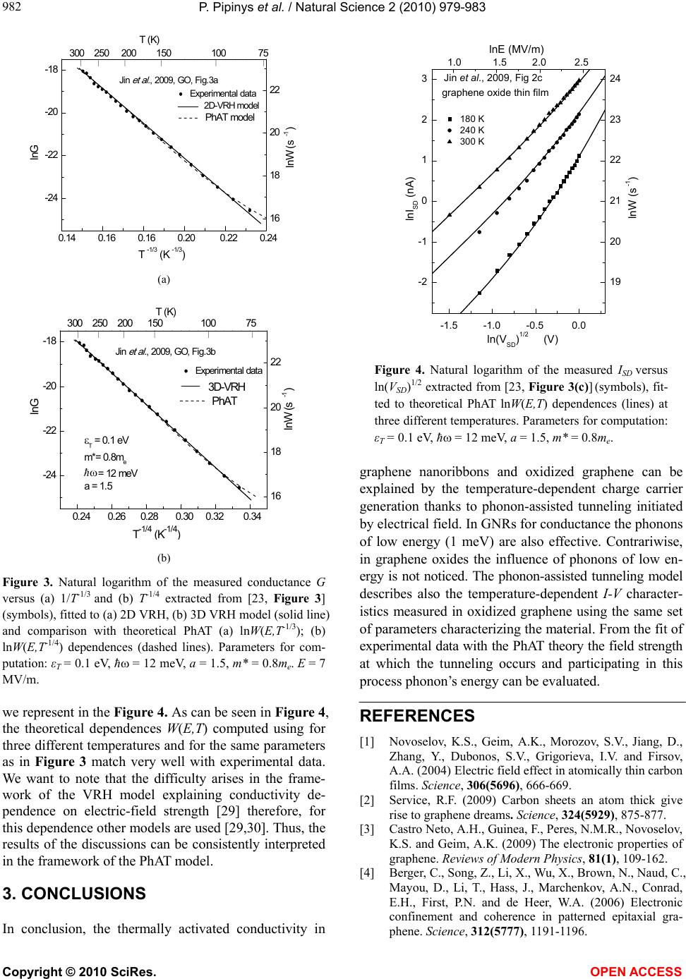 P. Pipinys et al. / Natural Science 2 (2010) 979-983 Copyright © 2010 SciRes. OPEN ACCESS 982 -24 -22 -20 -18 16 18 20 22 lnG T -1/3 (K -1/3) Experimental data 2D-VRH model PhAT model Jin et al. , 2009, GO, Fig.3a 0.14 0.16 0.16 0.20 0.22 0.24 lnW (s-1) (a) 300 250 200 150 100 75 T (K) (a) -24 -22 -20 -18 16 18 20 22 lnG T-1/4 ( K-1/4 ) Experimental data 3D-VRH PhAT Jin et al. , 2009, GO, Fig.3b T = 0.1 eV m*= 0.8me hw = 12 meV a = 1.5 0.24 0.26 0.28 0.30 0.32 0.34 T (K) lnW (s-1) 300 250 200 150 100 75 ћ (b) Figure 3. Natural logarithm of the measured conductance G versus (a) 1/T-1/3 and (b) T-1/4 extracted from [23, Figure 3] (symbols), fitted to (a) 2D VRH, (b) 3D VRH model (solid line) and comparison with theoretical PhAT (a) lnW(E,T-1/3); (b) lnW(E,T-1/4) dependences (dashed lines). Parameters for com- putation: εT = 0.1 eV, ћ = 12 meV, a = 1.5, m* = 0.8me. E = 7 MV/m. we represent in the Figure 4. As can be seen in Figure 4, the theoretical dependences W(E,T) computed using for three different temperatures and for the same parameters as in Figure 3 match very well with experimental data. We want to note that the difficulty arises in the frame- work of the VRH model explaining conductivity de- pendence on electric-field strength [29] therefore, for this dependence other models are used [29,30]. Thus, the results of the discussions can be consistently interpreted in the framework of the PhAT model. 3. CONCLUSIONS In conclusion, the thermally activated conductivity in -2 -1 0 1 2 3 19 20 21 22 23 24 lnISD (nA) ln(VSD)1/2 (V) 180 K 240 K 300 K Jin et al., 2009, Fig 2c lnE (MV/m) graphene oxide thin film -1.5 -1.0 -0.5 0.0 lnW (s -1) 1.0 1.5 2.0 2.5 Figure 4. Natural logarithm of the measured ISD versus ln(VSD)1/2 extracted from [23, Figure 3(c)] (symbols), fit- ted to theoretical PhAT lnW(E,T) dependences (lines) at three different temperatures. Parameters for computation: εT = 0.1 eV, ћ = 12 meV, a = 1.5, m* = 0.8me. graphene nanoribbons and oxidized graphene can be explained by the temperature-dependent charge carrier generation thanks to phonon-assisted tunneling initiated by electrical field. In GNRs for conductance the phonons of low energy (1 meV) are also effective. Contrariwise, in graphene oxides the influence of phonons of low en- ergy is not noticed. The phonon-assisted tunneling model describes also the temperature-dependent I-V character- istics measured in oxidized graphene using the same set of parameters characterizing the material. From the fit of experimental data with the PhAT theory the field strength at which the tunneling occurs and participating in this process phonon’s energy can be evaluated. REFERENCES [1] Novoselov, K.S., Geim, A.K., Morozov, S.V., Jiang, D., Zhang, Y., Dubonos, S.V., Grigorieva, I.V. and Firsov, A.A. (2004) Electric field effect in atomically thin carbon films. Science, 306(5696), 666-669. [2] Service, R.F. (2009) Carbon sheets an atom thick give rise to graphene dreams. Science, 324(5929), 875-877. [3] Castro Neto, A.H., Guinea, F., Peres, N.M.R., Novoselov, K.S. and Geim, A.K. (2009) The electronic properties of graphene. Reviews of Modern Physics, 81(1), 109-162. [4] Berger, C., Song, Z., Li, X., Wu, X., Brown, N., Naud, C., Mayou, D., Li, T., Hass, J., Marchenkov, A.N., Conrad, E.H., First, P.N. and de Heer, W.A. (2006) Electronic confinement and coherence in patterned epitaxial gra- phene. Science, 312(5777), 1191-1196.  P. Pipinys et al. / Natural Science 2 (2010) 979-983 Copyright © 2010 SciRes. OPEN ACCESS 983 983 [5] Han, M.Y., Özyilmaz, B., Zhang, Y. and Kim, P. (2007) Energy band-gap engineering of graphene nanoribbons. Physical Review Letters, 98(20), 206805. [6] Yan, Q., Huang, B., Yu, J., Zheng, F., Zang, J., Wu, J., Gu, B.-L., Liu, F. and Duan, W. (2007) Intrinsic current- voltage characteristics of graphene nanoribbon transis- tors and effect of edge doping. Nano Letters, 7(6), 1469- 1473. [7] Murali, R., Yang, Y., Brenner, K., Beck, T. and Meindl, J.D. (2009) Breakdown current density of graphene nanoribbons. Applied Physics Letters, 94(24), 243114. [8] Li, Z., Qian, H., Wu, J., Gu, B.-L. and Duan, W. (2008) Role of symmetry in the transport properties of graphene nanoribbons under bias. Physical Review Letters, 100 (20), 206802. [9] Rosales, L., Orellana, P., Barticevic, Z. and Pacheco, M. (2008) Transport properties of graphene nanoribbon het- erostructures. Microelectronics Journal, 39(3-4), 537-540. [10] Rigo, V.A., Martins, T.B., da Silva, A.J.R., Fazzio, A. and Miwa, R.H. (2009) Electronic, structural, and transport properties of Ni-doped graphene nanoribbons. Physical Review B, 79(7), 075435. [11] Sinitskii, A., Fursina, A.A., Kosynkin, D.V., Higginbotham, A.L., Natelson, D. and Tour, J.M. (2009) Electronic transport in monolayer graphene nanoribbons produced by chemical unzipping of carbon nanotubes. Applied Physics Letters, 95(25), 253108. [12] Xie, Y.E., Chen, Y.P. and Zhong, J.X. (2009) Electron transport of folded graphene nanoribbons. Journal of Ap- plied Physics, 106(10), 103714. [13] Han, M.Y., Brant, J.C. and Kim. P. (2010) Electron transport in disordered graphene nanoribbons. Physical Review Letters, 104(5), 056801. [14] Zhang, Y.-Y., Hu, J.-P., Xie, X.C., Liu, W.M. (2009) Ab- normal electronic transport in disordered graphene nano- ribbon. Physica B: Condensed Matter, 404(16), 2259- 2262. [15] Molitor, F., Stampfer, C., Güttinger, J., Jacobsen, A., Ihn, T. and Ensslin, K. (2010) Energy and transport gaps in etched graphene nanoribbons. Semiconductor Science and Technology, 25(3), 034002. [16] Ihnatsenka, S. and Kirczenow, G. (2009) Conductance quantization in strongly disordered graphene ribbons. Physical Review B, 80(20), 201407(R). [17] Lian, Ch., Tahy, K., Fang, T., Li, G., Xing, H.G. and Jena, D. (2010) Quantum transport in graphene nanoribbons patterned. Applied Physics Letters, 96(10), 103109. [18] Jiménez, D. (2008) A current-voltage model for Schot- tky-barrier graphene-based transistors. Nanotechnology, 19(34), 345204. [19] Wakabayashi, K., Takane, Y., Yamamoto, M. and Sigrist, M. (2009) Electronic transport properties of graphene nanoribbons. New Journal of Physics, 11 (9) , 095016. [20] Jung, I., Dikin, D.A., Piner, R.D. and Ruoff, R.S. (2008) Tunable electrical conductivity of individual graphene oxide sheets reduced at “Low” temperatures. Nano Let- ters, 8(12), 4283-4287. [21] Gómez-Navarro, C., Weitz, R.T., Bittner, A.M., Scolari, M., Mews, A., Burghard, M. and Kern, K. (2007) Elec- tronic transport properties of individual chemically re- duced graphene oxide sheets. Nano Letters, 7(11), 3499- 3503. [22] Kaiser, A.B., Gómez-Navarro, C., Sundaram, R.S., Burghard, M. and Kern, K. (2009) Electrical conduction mechanism in chemically derived graphene monolayers. Nano Letters, 9(5), 1787-1792. [23] Jin, M., Jeong, H.-K., Yu, W.J., Bae, D.J., Kang, B.R. and Lee, Y.H. (2009) Graphene oxide thin film field effect transistors without reduction. Journal of Physics D: Ap- plied Physics, 42(13), 135109. [24] Shao, Q., Liu, G., Teweldebrhan, D. and Balandin, A.A. (2008) High-temperature quenching of electrical resis- tance in graphene interconnects. Applied Physics Letters, 92(20), 202108. [25] Pipinys, P., Rimeika, A. and Lapeika, V. (2004) DC con- duction in polymers under high electric field. Journal of Physics D: Applied Physics, 37(6), 828-831. [26] Pipinys, P. and Kiveris, A. (2008) Phonon-assisted tun- nelling in electrical conductivity of individual carbon nanotubes and networks ones. Physica B: Condensed Matter, 403(19-20), 3730-3733. [27] Kiveris, A., Kudžmauskas Š. and Pipinys P. (1976) Re- lease of electrons from traps by an electric field with phonon participation. Physica Status Solidi A, 37(1), 321- 327. [28] Popov, V.N., Henrard, L. and Lambin, P. (2005) Elec- tron-phonon and electron-photon interactions and reso- nant Raman scattering from the radial-breathing mode of single-walled carbon nanotubes. Physical Review B, 72(3), 035436. [29] Wang, D.P., Feldman, D.E., Perkins, B.R., Yin, A.J., Wang, G.H., Xu, J.M. and Zaslavsky, A. (2007) Hopping conduction in disordered carbon nanotubes. Solid State Communication, 142(5), 287-291. [30] Kaiser, A.B. and Park, Y.W. (2005) Current-voltage characteristics of conducting polymers and carbon nano- tubes. Synthetic Metals, 152(1-3), 181-184. |