

Paper Menu >>
Journal Menu >>
 Circuits and Systems, 2013, 4, 83-88 http://dx.doi.org/10.4236/cs.2013.41013 Published Online January 2013 (http://www.scirp.org/journal/cs) Universal Current-Mode Biquad Employing Dual Output Current Conveyors and MO-CCCA with Grounded Passive Elements Kasim Karam Abdalla Department of Electrical Engineering, Engineering Colloge, University of Babylon, Hilla, Iraq Email: kasimkaa[email protected] Received May 17, 2012; revised November 6, 2012; accepted November 13, 2012 ABSTRACT A new universal multiple input multiple output (MIMO) type current-mode biquad employing two dual output current conveyors (DOCCII), one multiple output current controlled current amplifier (MOCCCA) and four passive grounded elements is proposed which can realize all the five basic filtering functions namely, low - pass (LP), high - pass (HP), band - pass (BP), band - stop (BR) and all - pass (AP) in current mode from the same configuration. The centre frequency o can be set by the passive elements of the circuit and the quality factor is electronically tunable through bias currents of the MOCCCA. Therefore, the biquad filter has independent tenability for the o Q o and Q. The active and passive sensitivities of and o o Qo are low. The workability of the new configuration has been demonstrated by PSPICE simulation results based upon a CMOS CCII in 0.35 μm technology. Keywords: Current-Mode Filters; Current Conveyors; Analog Circuit Design; CMOS Circuits 1. Introduction Recently, Chunhua, Hiaguang and Yan presented two new universal multiple input single output (MISO) cur- rent-mode (CM) biquadatic filters using one MOCCCA, two grounded capacitors (GC) and two grounded resis- tors (GR) and realize all the five generic filter responses in CM (i.e. with current as input and current as output) [1]. The purpose of this paper is to introduce a new con- figuration which although uses exactly same number of active and passive components but in contrast to the cir- cuit of reference [1] realizes a MIMO-type biquad and hence, does not require any additional hardware to du- plicate/invert current inputs which is required in case of MISO-type filters of [1]. In the literature there are SIMO-type filter circuits which have three active devices but suffer from the in- dependent tunability as in [2-5] or have more passive or active elements as in [4-9]. The circuits in [10-12] need double inputs and outputs to realize all five generic filters. The circuit in [13] has two MO-CCCIIs and one DO- CCCII, the draw back of this circuit is the control cur- rents oi are temperature dependent. The cir- cuit in [14] has two MO-CCCIIs and one MOCCCA but realizes only SIMO-type biquad. 2. The Proposed Configuration The proposed configuration is shown in Figure 1. Assuming the CCIIs to be characterized by ,1,2,3Ii 000 100 010 YY XX ZZ I V VI I V (1) The symbolic notation of MO-CCCA is given in Fig- ure 2(a), where i represent input, 1oon I Iare n out- puts respectively, and IA and IB denote DC bias currents. Figure 2(b) is a CMOS realization of MO-CCCA. Here Ii denotes the input signal; Io1, Io2, Io3 are the three output currents, respectively. If the channel lengths of M5-M8 are all n times of that of M4, and the channel size of M17 is n times that of M18, namely 54 64 74 84 1718 , MM MM MM MMM M WL WL WL WLWL WL WL WLWLWLn the output current expressions can be obtained as 12 2 B o ooni A nI I II KI I (2) C opyright © 2013 SciRes. CS 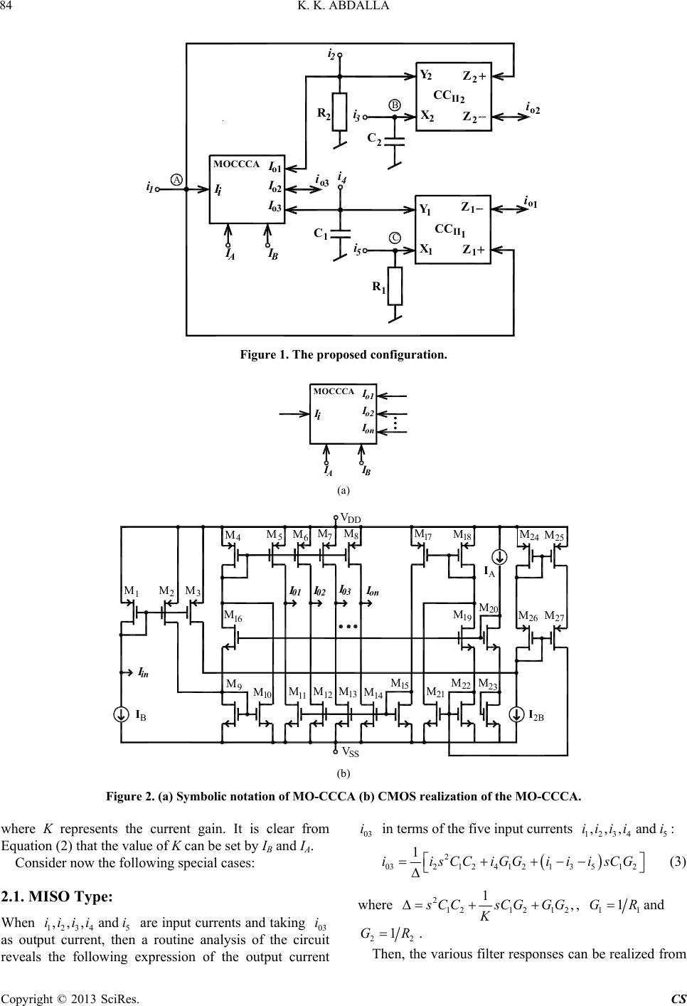 K. K. ABDALLA 84 II CC II CC MOCCCA 1 C io3 R1 2 R 2 C Y 1 X1 Y 2 X2 i3 i4 A B io1 Z1 Z1 Z2 Z2 C1 2 i2 i5 i1Ii Io1 Io2 Io3 io2 IB IA Figure 1. The proposed configuration. MOCCCA Ii Io1 Io2 Ion IB IA (a) M M M M M M 8 11 1 1 34 5 6 7 M27 M6 M M 5 2 M1M3 M4 2 M MMM 910111 1 0 M MM M 1 12 78 9 4 M2 M M2 2 5 6 3 M MM 22 2 12 VSS VDD IA IB Iin I01 I02I03Ion I2B (b) Figure 2. (a) Symbolic notation of MO-CCCA (b) CMOS realization of the MO-CCCA. where K represents the current gain. It is clear from Equation (2) that the value of K can be set by IB and IA. Consider now the following special cases: 2.1. MISO Type: When 1234 5 are input currents and taking 03 as output current, then a routine analysis of the circuit reveals the following expression of the output currt 03 i in terms of the five input currend ,,, andiiii ii en nts 1234 5 ,,, aiiii i: 2 0321 24 1 21351 2 1 iisCCiGGiiisCG (3) where 2 1212 12 1, s CCsCG GG K , 11 1GRand 22 1GR. Then, the various filter responses can be realized from Copyright © 2013 SciRes. CS 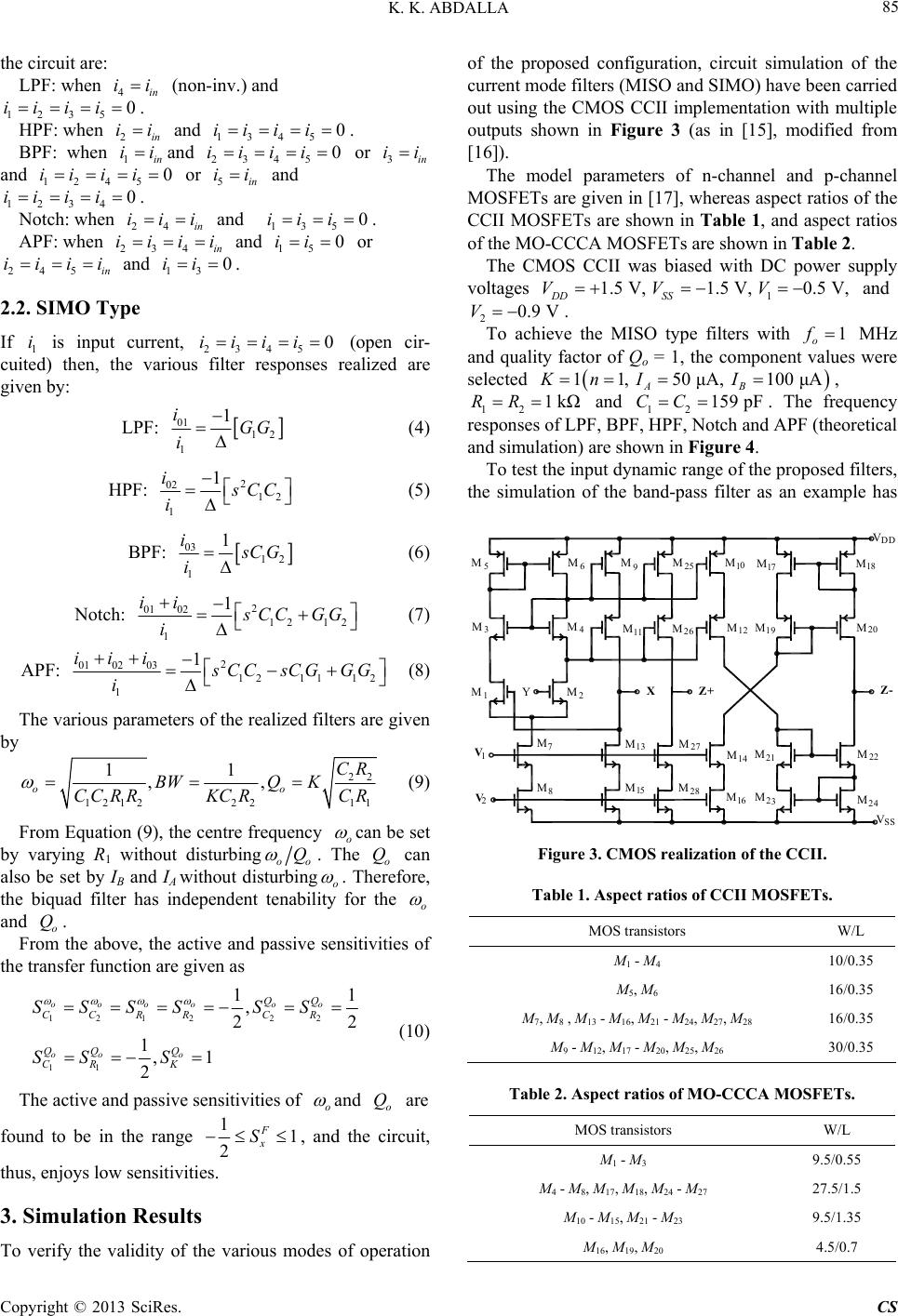 K. K. ABDALLA 85 the circuit are: LPF: when (non-inv.) and . 4in ii 0 ii 0 ii 12 ii 35 HPF: when and 2in ii1 ii 345 0 . BPF: when and 451in 23 iiiiii 3in ii or and or 12 ii 45 0ii 5 i in i and . 1 ii 234 Notch: when and . 0i iii i 5 0i ii 15 0ii i0 ii 24in ii 13 APF: when 234 and or and . ii in 13 0ii 245in iiii 2.2. SIMO Type If 1 is input current, 2345 (open cir- cuited) then, the various filter responses realized are given by: ii LPF: 12 1GG 01 1 i i (4) HPF: 2 12 1 02 1 i s CC i (5) BPF: 12 1 03 1 i s CGi (6) Notch: 2 01 02 1 1 ii 12 12 s CC GG i (7) APF: 2 01 0203 12 1 1 ii i 1112 s CC s i CG GG (8) The various parameters of the realized filters are given by 22 11 CR KCR 1212 22 11 ,, oo BW Q CC RRKC R (9) From Equation (9), the centre frequency o can be set by varying R1 without disturbingoo Q . The o can also be set by IB and IA without disturbingo Q . Therefore, the biquad filter has independent tenability for the o and . o From the above, the active and passive sensitivities of the transfer function are given as Q 1212 11 , 1,1 2 oooo oo o CCRR QQ Q K CR SSSS SSS 22 11 22 oo QQ CR SS o (10) The active and passive sensitivities of and are o Q found to be in the range 11 2x S 1 1.5 V, 1.5 V, 0.5 V, DD SS VVV F, and the circuit, thus, enjoys low sensitivities. 3. Simulation Results To verify the validity of the various modes of operation of the proposed configuration, circuit simulation of the current mode filters (MISO and SIMO) have been carried out using the CMOS CCII implementation with multiple outputs shown in Figure 3 (as in [15], modified from [16]). The model parameters of n-channel and p-channel MOSFETs are given in [17], whereas aspect ratios of the CCII MOSFETs are shown in Table 1, and aspect ratios of the MO-CCCA MOSFETs are shown in Table 2. The CMOS CCII was biased with DC power supply voltages 20.9 VV and 1f . To achieve the MISO type filters with o MHz and quality factor of Qo = 1, the component values were selected 11, 50 μA, 100 μA AB KnI I 1 kΩRR, 12 159 pFCC and 12 . The frequency responses of LPF, BPF, HPF, Notch and APF (theoretical and simulation) are shown in Figure 4. To test the input dynamic range of the proposed filters, the simulation of the band-pass filter as an example has VSS Z- Z+ X Y VDD 1 2 4 3 0 M M MM MMMM M MMMM M MMM MMM MM M MM M M M 12 34 56 8 910 1 1 1 1 1 1 1 1 1 2 2 2 2 2 2 2 2 2 3 4 5 6 78 9 12 V V 2 1 5 6 7 8 7 Figure 3. CMOS realization of the CCII. Table 1. Aspect ratios of CCII MOSFETs. MOS transistors W/L M1 - M4 10/0.35 M5, M6 16/0.35 M7, M8 , M13 - M16, M21 - M24, M27, M28 16/0.35 M9 - M12, M17 - M20, M25, M26 30/0.35 Table 2. Aspect ratios of MO-CCCA MOSFETs. MOS transistors W/L M1 - M3 9.5/0.55 M4 - M8, M17, M18, M24 - M27 27.5/1.5 M10 - M15, M21 - M23 9.5/1.35 M16, M19, M20 4.5/0.7 Copyright © 2013 SciRes. CS 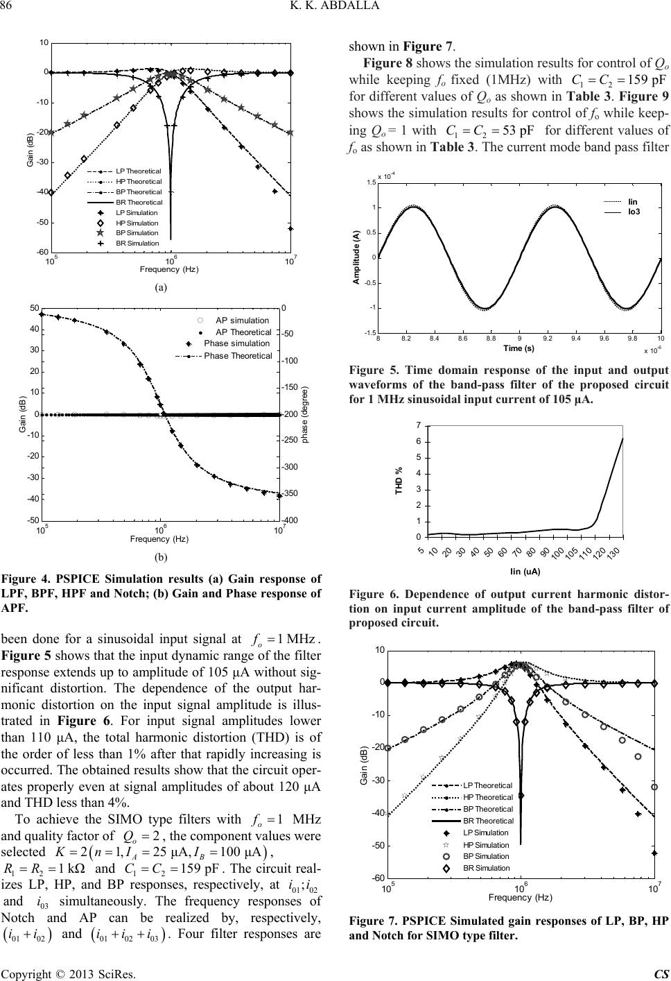 K. K. ABDALLA 86 10 5 10 6 10 7 -60 -50 -40 -30 -20 -10 0 10 Frequency (Hz) Gain (dB ) LP Theoretical HP Theo retical BP Theoretical BR Theoretical LP Simulatio n HP Simulation BP Simulation BR Simulation (a) 10 5 10 6 10 7 -50 -40 -30 -20 -10 0 10 20 30 40 50 Frequency (Hz) Gain (dB ) AP si mulation AP Theoreti cal p hase ( de g ree ) -400 -350 -300 -250 -200 -150 -100 -50 0 P has e simul ati on P has e Theoreti c al (b) Figure 4. PSPICE Simulation results (a) Gain response of LPF, BPF, HPF and Notch; (b) Gain and Phase response of APF. been done for a sinusoidal input signal at o1 MHzf . Figure 5 shows that the input dynamic range of the filter response extends up to amplitude of 105 μA without sig- nificant distortion. The dependence of the output har- monic distortion on the input signal amplitude is illus- trated in Figure 6. For input signal amplitudes lower than 110 μA, the total harmonic distortion (THD) is of the order of less than 1% after that rapidly increasing is occurred. The obtained results show that the circuit oper- ates properly even at signal amplitudes of about 120 μA and THD less than 4%. To achieve the SIMO type filters with o1f MHz and quality factor of , the component values were selected , 12 and 12 CC . The circuit real- izes LP, HP, and BP responses, respectively, at 0102 03 simultaneously. The frequency responses of Notch and AP can be realized by, respectively, Figure Figure 8 shows th 2 o Q 100 μAI ;ii filter responses are shown in 7. e simulation results for control of Qo w able 3. Figure 9 21,KnI RR and 01 ii 01 02 03 iii 25 μA, AB 159 pF . Four 1 kΩ i 02 and hile keeping fo fixed (1MHz) with 12 159 pFCC for different values of Qo as shown in T shows the simulation results for control of fo while keep- ing Qo = 1 with 12 53 pFCC for different values of fo as shown in Ta nt mode band pass filter ble 3. The curre 88.2 8.4 8.6 8.8 99.2 9.4 9.6 9.810 x 10 -6 -1.5 -1 -0.5 0 0.5 1 1.5 x 10 -4 Tim e ( s) Ampl it ude (A) Iin Io3 Figure 5. Time domain response of the input and output waveforms of the band-pass filter of the proposed circuit for 1 MHz sinusoidal input current of 105 μA. 7 0 1 2 3 4 5 6 5102030405060708090 100 105 110 120 130 Iin (uA) THD % Figure 6. Dependence of output current harmonic- distor tion on input current amplitude of the band-pass filter of proposed circuit. 10 0 -10 -20 -30 10 5 10 6 10 7 -60 -50 -40 Frequency (Hz) Gain (dB ) LP Theoretical HP Theoretical BP Theoretical BR Theoretical LP Simulation HP Simulation BP Simulation BR Simulation Figure 7. PSPICE Simulated gain responses of LP, BP, HP and Notch for SIMO type filter. Copyright © 2013 SciRes. CS 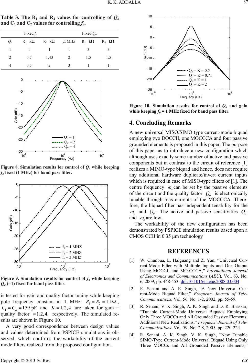 K. K. ABDALLA 87 Table 3. The R1 and R2 values for controlling of Qo and C and C values for cont 1 2rolling fo. Fixed fo Fixed Qo Qo 2 kΩ MHz R2 kΩ R1 kΩ Rfo R1 kΩ 1 1 1 3 3 1.43 1 2 0.7 2 1.5 1.5 4 0.5 2 3 1 1 10 5 10 6 10 7 -30 -25 -20 -15 -10 -5 0 Frequen c y (Hz) Gain (dB ) Qo = 1 Qo = 2 Qo = 4 Q o = 1 Q o = 2 Q o = 4 Figure 8. Simulation results for control of Qo while keeping f fixed (1 MHz) for band pass filter. o 10 5 10 6 10 7 -30 -25 -20 -15 -10 -5 0 Frequenc y (Hz ) Gain (dB ) fo =1 MHz fo =2 MHz fo =3 MHz f o = 1 MHZ f o = 2 MHZ f o = 3 MHZ Figure 9. Simulation results for control of fo while keeping Q (=1) fixed for band pass filter. tor tuning while keeping RR ine 10 o is tested for gain and quality fac pole frequency constant at 1 MHz. 12 1 kΩ, 12 159 pFCC and 1,2,4K are taken for gain = quality factor 1, 2, 4, respectively. The simulated re- sults are shown Figur . A very good correspondence between design values and values determined from PSPICE simulations is ob- served, which confirms the workability of the current mode filters realized from the proposed configuration. 10 5 10 6 10 7 -25 -20 -15 -10 -5 0 5 10 Frequecy (Hz ) Gain (dB) Qo=K=0.5 Qo=K=0.71 Qo=K=1 Qo=K=2 Q o = K = 0.5 Q o = K = 0.71 Q o = K = 1 Q o = K = 2 Figure 10. Simulation results for control of Qo and gain while keeping fo = 1 MHz fixed for band pass filter. type current-mode biquad OCCCA and four passive 4. Concluding Remarks A new universal MISO/SIMO employing two DOCCII, one M grounded elements is proposed in this paper. The purpose of this paper as to introduce a new configuration which although uses exactly same number of active and passive components but in contrast to the circuit of reference [1] realizes a MIMO-type biquad and hence, does not require any additional hardware duplicate/invert current inputs which is required in case of MISO-type filters of [1]. The centre frequency o can be set by the passive elements of the circuit and the quality factor o Q is electronically tunable through b currents of the MOCCCA. There- fore, the biquad filter has independent tenability for the o ias and o Q. The active and passive sensitivities o Q and o are low. The workability of the new configuration has be demotrated by PS en nsPICE simulation results based upon a C S [1] W. Chunbua, n, “Universal Cur- rent-Mode Filts and One Output MOS CCII in 0.35 μm technology REFERENCE L. Haiguang and Z. Ya er with Multiple Input Using MOCCII and MO-CCCA,” International Journal of Electronics and Communications (AEU), Vol. 63, No. 6, 2009, pp. 448-453. doi:10.1016/j.aeue.2008.03.004 [2] R. Senani and A. K. Singh, “A New Universal Cur- rent-Mode Biquad Filter,” Frequenz: Journal of Tele- ying y Three MOCCs and All Grounded Passive Elements,” Communications, Vol. 56, No. 1-2, 2002, pp. 55-59. [3] R. Senani, V. K. Singh, A. K. Singh and D. R. Bhaskar, “Tunable Current-Mode Universal Biquads Emplo Only Three MOCCs and All Grounded Passive Elements: Additional New Realizations,” Frequenz: Journal of Tele- Communications, Vol. 59, No. 7-8, 2005, pp. 220-224. [4] R. Senani, A. K. Singh, V. K. Singh, “New Tunable SIMO-Type Current-Mode Universal Biquad Using Onl Copyright © 2013 SciRes. CS 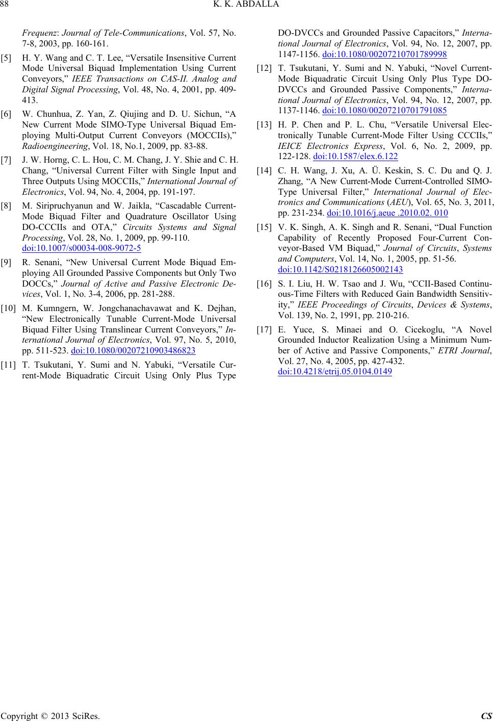 K. K. ABDALLA Copyright © 2013 SciRes. CS 88 sactions on CAS-II. Analog and g Multi-Output Current Conveyors (MOCCIIs),” d Signal Frequenz: Journal of Tele-Communications, Vol. 57, No. 7-8, 2003, pp. 160-161. [5] H. Y. Wang and C. T. Lee, “Versatile Insensitive Current Mode Universal Biquad Implementation Using Current Conveyors,” IEEE Tran Digital Signal Processing, Vol. 48, No. 4, 2001, pp. 409- 413. [6] W. Chunhua, Z. Yan, Z. Qiujing and D. U. Sichun, “A New Current Mode SIMO-Type Universal Biquad Em- ployin Radioengineering, Vol. 18, No.1, 2009, pp. 83-88. [7] J. W. Horng, C. L. Hou, C. M. Chang, J. Y. Shie and C. H. Chang, “Universal Current Filter with Single Input and Three Outputs Using MOCCIIs,” International Journal of Electronics, Vol. 94, No. 4, 2004, pp. 191-197. [8] M. Siripruchyanun and W. Jaikla, “Cascadable Current- Mode Biquad Filter and Quadrature Oscillator Using DO-CCCIIs and OTA,” Circuits Systems an Processing, Vol. 28, No. 1, 2009, pp. 99-110. doi:10.1007/s00034-008-9072-5 [9] R. Senani, “New Universal Current Mode Biquad Em- ploying All Grounded Passive Components but DOCCs,” Journal of Active and Only Two Passive Electronic De- onveyors,” In- vices, Vol. 1, No. 3-4, 2006, pp. 281-288. [10] M. Kumngern, W. Jongchanachavawat and K. Dejhan, “New Electronically Tunable Current-Mode Universal Biquad Filter Using Translinear Current C ternational Journal of Electronics, Vol. 97, No. 5, 2010, pp. 511-523. doi:10.1080/00207210903486823 [11] T. Tsukutani, Y. Sumi and N. Yabuki, “Versatile Cur- rent-Mode Biquadratic Circuit Using Only Plus Type DO-DVCCs and Grounded Passive Capacitors,” Interna- tional Journal of Electronics, Vol. 94, No. 12, 2007, pp. 1147-1156. doi:10.1080/00207210701789998 [12] T. Tsukutani, Y. Sumi and N. Yabuki, “Novel Current- Mode Biquadratic Circuit Using Only Plus Type DO- DVCCs and Grounded Passive Components,” Interna- tional Journal of Electronics, Vol. 94, No. 12, 2007, pp. 1137-1146. doi:10.1080/00207210701791085 [13] H. P. Chen and P. L. Chu, “Versatile Universal Elec- tronically Tunable Current-Mode Filter Using CCCIIs,” IEICE Electronics Express, Vol. 6, No. 2, 2009, pp. 122-128. doi:10.1587/elex.6.122 [14] C. H. Wang, J. Xu, A. Ü. Keskin, S. C. Du and Q. J. Zhang, “A New Current-Mode Current-Controlled SIMO- Type Universal Filter,” International Journal of Elec- tronics and Communications (AEU), Vol. 65, No. 3, 2011, pp. 231-234. doi:10.1016/j.aeue .2010.02. 010 [15] V. K. Singh, A. K. Singh and R. Senani, “Dual Function Capability of Recently Proposed Four-Current Con- veyor-Based VM Biquad,” Journal of Circuits, Systems and Computers, Vol. 14, No. 1, 2005, pp. 51-56. doi:10.1142/S0218126605002143 [16] S. I. Liu, H. W. Tsao and J. Wu, “CCII-Based Continu- cekoglu, “A Novel ous-Time Filters with Reduced Gain Bandwidth Sensitiv- ity,” IEEE Proceedings of Circuits, Devices & Systems, Vol. 139, No. 2, 1991, pp. 210-216. [17] E. Yuce, S. Minaei and O. Ci Grounded Inductor Realization Using a Minimum Num- ber of Active and Passive Components,” ETRI Journal, Vol. 27, No. 4, 2005, pp. 427-432. doi:10.4218/etrij.05.0104.0149 |