

Paper Menu >>
Journal Menu >>
 Circuits and Systems, 2013, 4, 44-48 http://dx.doi.org/10.4236/cs.2013.41008 Published Online January 2013 (http://www.scirp.org/journal/cs) Voltage-Mode Universal Biquad Filter Employing Single Voltage Differencing Differential Input Buffered Amplifier Kanhaiya Lal Pushkar1, Data Ram Bhaskar2*, Dinesh Prasad2 1Department of Electronics and Communication Engineering, Maharaja Agrasen Institute of Technology, New Delhi, India 2Department of Electronics and Communication Engineering, Faculty of Engineering and Technology, Jamia Millia Islamia, New Delhi, India Email: klpushkar@rediffmail.com, *[email protected], [email protected] Received October 24, 2012; revised November 23, 2012; accepted November 30, 2012 ABSTRACT A new multi function voltage-mode universal biquadratic filter using single Voltage Differencing Differential Input Buffered Amplifier (VD-DIBA), two capacitors and one resistor is proposed. The proposed configuration has four in- puts and one output and can realize all the five standard filters from the same circuit configuration. The presented bi- quad filter offers low active and passive sensitivities. The validity of proposed universal biquadratic filter has been veri- fied by SPICE simulation using 0.35 µm MIETEC technology. Keywords: Voltage Differencing Differential Input Buffered Amplifier; Analog Filter; Voltage-Mode 1. Introduction Recently, attention has been devoted to the design of multi-input single output (MISO) or single input multi- output (SIMO) current-mode or voltage-mode universal biquadratic filters because of their versatility and flexi- bility for practical applications as the same circuit topol- ogy can be employed for different filter responses. Several voltage-mode/current-mode universal biquadratic filters using different types of single active building block/device have been presented in [1-8]. In reference [9] number of new active building blocks have been introduced, VD- DIBA is one of them which is emerging as a flexible and versatile active element for analog signal processing. The applications, advantages and usefulness of VD-DIBA have been recognized in [10,11]. They have been used in the realization of first order all pass filter [10], and in the re- alization of grounded and floating inductances as pre- sented in [11]. The various filter configurations proposed in [1-8] and [10,11] although employ single active de- vice/element, but use two to four capacitors and two to four resistors. Therefore, the purpose of this paper is to introduce a new voltage-mode universal biquadratic filter using single VD-DIBA, two capacitors and only one re- sistor. The proposed configuration has four inputs and one output and can realize all the five standard filters (low pass (LPF), high pass (HPF), band pass (BPF), band reject (BRF) and all pass (APF)) by proper selection of input voltages from the same circuit configuration without al- tering the circuit topology. The active and passive sensi- tivities of the realized filters are low. The validity of the proposed configuration has been verified by SPICE simu- lation using 0.35 µm MIETC technology. 2. The Proposed Biquadratic Filter Configuration The symbolic notation and equivalent model of the VD- DIBA (+) are shown in Figures 1(a) and (b) respectively [1]. The model includes two controlled sources: the cur- rent source controlled by differential voltage VV , with the transconductance m g , and the voltage source controlled by differential voltage z v VV 00000 00000 000 00000 00110 with the unity voltage gain. The VD-DIBA (+) can be described by the following set of equations: I V I V z z mm vv ww I V gg I V VI (1) The proposed voltage-mode universal biquadratic filter is shown in Figure 2. A routine circuit analysis of Figure 2 yields the fol- lowing expression for the output voltage in terms of the input voltages *Corresponding author. C opyright © 2013 SciRes. CS 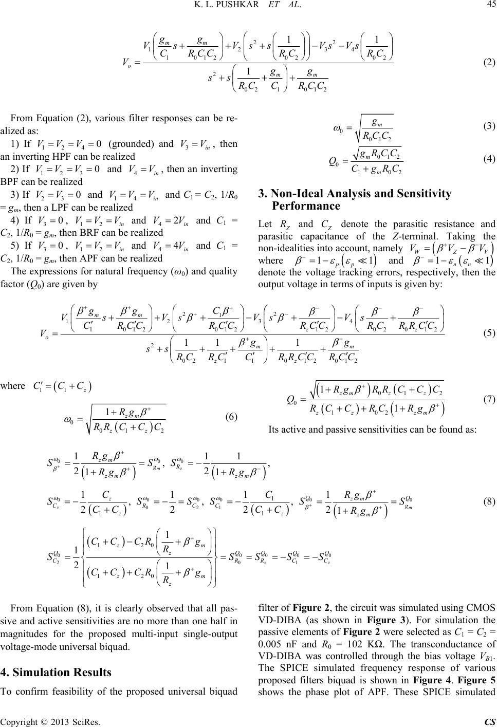 K. L. PUSHKAR ET AL. 45 22 12 1012 02 2 02 1012 1 mm o mm gg VsVss V CRCC RC Vgg ss RC CRCC 34 02 11 sVs RC 0VVV 3in V 0 VVV 4in VV 0 VVin V 0VVV 2in V 0VVV 4in V (2) From Equation (2), various filter responses can be re- alized as: 0 012 m g RCC 1) If 124 (grounded) and V, then an inverting HPF can be realized 2) If 123 and , then an inverting BPF can be realized 3) If 23 and 14 VV and C1 = C2, 1/R0 = gm, then a LPF can be realized 4) If 3 V, 12in and 4 V and C1 = C2, 1/R0 = gm, then BRF can be realized 5) If 3 V, 12in and 4 V and C1 = C2, 1/R0 = gm, then APF can be realized The expressions for natural frequency (ω0) and quality factor (Q0) are given by (3) 012 0 102 m m g RCC QCgRC (4) 3. Non-Ideal Analysis and Sensitivity Performance Let Z R and Z C WZV VVV denote the parasitic resistance and parasitic capacitance of the Z-terminal. Taking the non-idealities into account, namely where 11 pp and 11 nn denote the voltage tracking errors, respectively, then the output voltage in terms of inputs is given by: 22 1 1234 101201212 02012 2 02110 12012 11 1 mm zz mm zz gg C Vs VsVsVs CRCCRCCRCCRCR RCC gg ss RC RCCRRCCRCC 11 o V (5) where z CCC 0 1zm Rg RR CC C 01 2zz (6) 01 2 0 102 1 1 zmz z zz zm RgRR CCC QRC CRCRg (7) Its active and passive sensitivities can be found as: 000 0 1 120 111 ,, 22 11 1111 mz 00 000 021 0 2 0 11 12 0 ,, , 2222 1 1 1 21 z m zm gR zm zm QQ zm z g zm z Rg SSS Rg Rg Rg CC S R 00 0 0 1zz QQQQ RCC SSS CR CC zz zm zm z Q CR SSSSS CCCC Rg CC CRg R SS CC CRg (8) From Equation (8), it is clearly observed that all pas- sive and active sensitivities are no more than one half in magnitudes for the proposed multi-input single-output voltage-mode universal biquad. 4. Simulation Results To confirm feasibility of the proposed universal biquad filter of Figure 2, the circuit was simulated using CMOS VD-DIBA (as shown in Figure 3). For simulation the passive elements of Figure 2 were selected as C1 = C2 = 0.005 nF and R0 = 102 KΩ. The transconductance of VD-DIBA was controlled through the bias voltage VB1. The SPICE simulated frequency response of various proposed filters biquad is shown in Figure 4. Figure 5 shows the phase plot of APF. These SPICE simulated Copyright © 2013 SciRes. CS 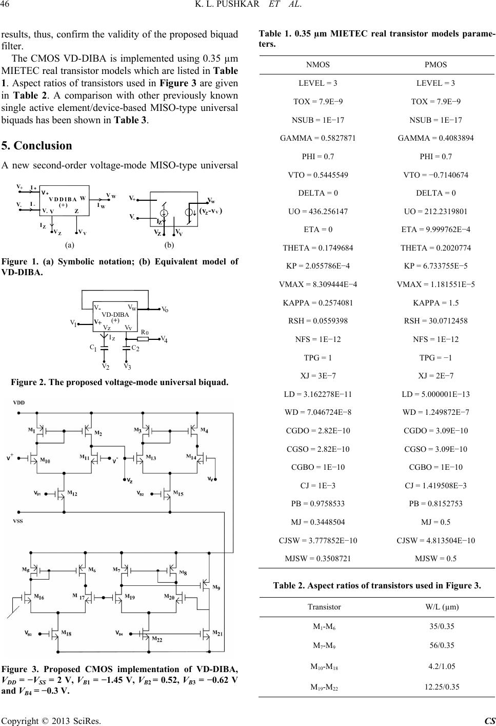 K. L. PUSHKAR ET AL. 46 results, thus, confirm the validity of the proposed biquad filter. The CMOS VD-DIBA is implemented using 0.35 µm MIETEC real transistor models which are listed in Table 1. Aspect ratios of transistors used in Figure 3 are given in Table 2. A comparison with other previously known single active element/device-based MISO-type universal biquads has been shown in Table 3. 5. Conclusion A new second-order voltage-mode MISO-type universal VDDI (+ BA ) Z IZ V- V+ I+ I- V VZ V+ V- W VV IW VW I Z V ZV V V + V - (v -v ) V Z V w (a) (b) Figure 1. (a) Symbolic notation; (b) Equivalent model of VD-DIBA. VD-DIBA +) Vv V w ( V- V +Vz V 1 V2V3 V 4 V o C1 Iz C2 R0 Figure 2. The proposed voltage-mode universal biquad. Figure 3. Proposed CMOS implementation of VD-DIBA, VDD = −VSS = 2 V, VB1 = −1.45 V, VB2 = 0.52, VB3 = −0.62 V and VB4 = −0.3 V. Table 1. 0.35 µm MIETEC real transistor models parame- ters. NMOS PMOS LEVEL = 3 LEVEL = 3 TOX = 7.9E−9 TOX = 7.9E−9 NSUB = 1E−17 NSUB = 1E−17 GAMMA = 0.5827871 GAMMA = 0.4083894 PHI = 0.7 PHI = 0.7 VTO = 0.5445549 VTO = −0.7140674 DELTA = 0 DELTA = 0 UO = 436.256147 UO = 212.2319801 ETA = 0 ETA = 9.999762E−4 THETA = 0.1749684 THETA = 0.2020774 KP = 2.055786E−4 KP = 6.733755E−5 VMAX = 8.309444E−4 VMAX = 1.181551E−5 KAPPA = 0.2574081 KAPPA = 1.5 RSH = 0.0559398 RSH = 30.0712458 NFS = 1E−12 NFS = 1E−12 TPG = 1 TPG = −1 XJ = 3E−7 XJ = 2E−7 LD = 3.162278E−11 LD = 5.000001E−13 WD = 7.046724E−8 WD = 1.249872E−7 CGDO = 2.82E−10 CGDO = 3.09E−10 CGSO = 2.82E−10 CGSO = 3.09E−10 CGBO = 1E−10 CGBO = 1E−10 CJ = 1E−3 CJ = 1.419508E−3 PB = 0.9758533 PB = 0.8152753 MJ = 0.3448504 MJ = 0.5 CJSW = 3.777852E−10 CJSW = 4.813504E−10 MJSW = 0.3508721 MJSW = 0.5 Table 2. Aspect ratios of transistors used in Figure 3. Transistor W/L (µm) M1-M6 35/0.35 M7-M9 56/0.35 M10-M18 4.2/1.05 M19-M22 12.25/0.35 Copyright © 2013 SciRes. CS 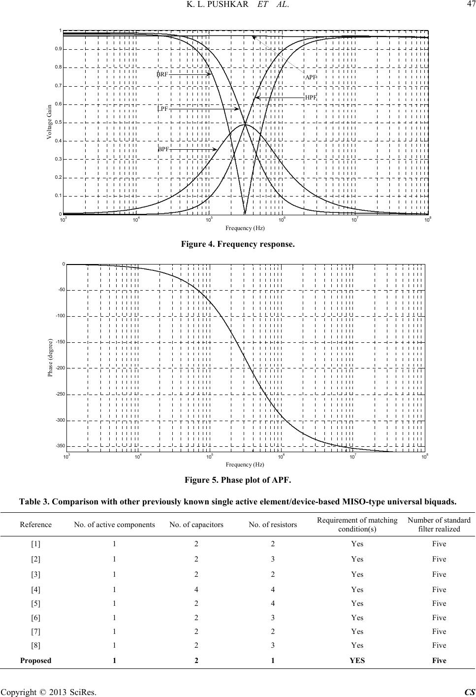 K. L. PUSHKAR ET AL. Copyright © 2013 SciRes. CS 47 10 3 10 4 10 5 10 6 10 7 10 8 0 0.1 0.2 0.3 0.4 0.5 0.6 0.7 0.8 0.9 1 Frequency (Hz) Voltage Gain BRF BP F LPF APF HPF Figure 4. Frequency response. 10 3 10 4 10 5 10 6 10 7 10 8 -350 -300 -250 -200 -150 -100 -50 0 Frequency (Hz) Phase (degree) Figure 5. Phase plot of APF. Table 3. Comparison with other previously known single active element/device-based MISO-type universal biquads. Reference No. of active components No. of capacitors No. of resistors Requirement of matching condition(s) Number of standard filter realized [1] 1 2 2 Yes Five [2] 1 2 3 Yes Five [3] 1 2 2 Yes Five [4] 1 4 4 Yes Five [5] 1 2 4 Yes Five [6] 1 2 3 Yes Five [7] 1 2 2 Yes Five [8] 1 2 3 Yes Five Proposed 1 2 1 YES Five 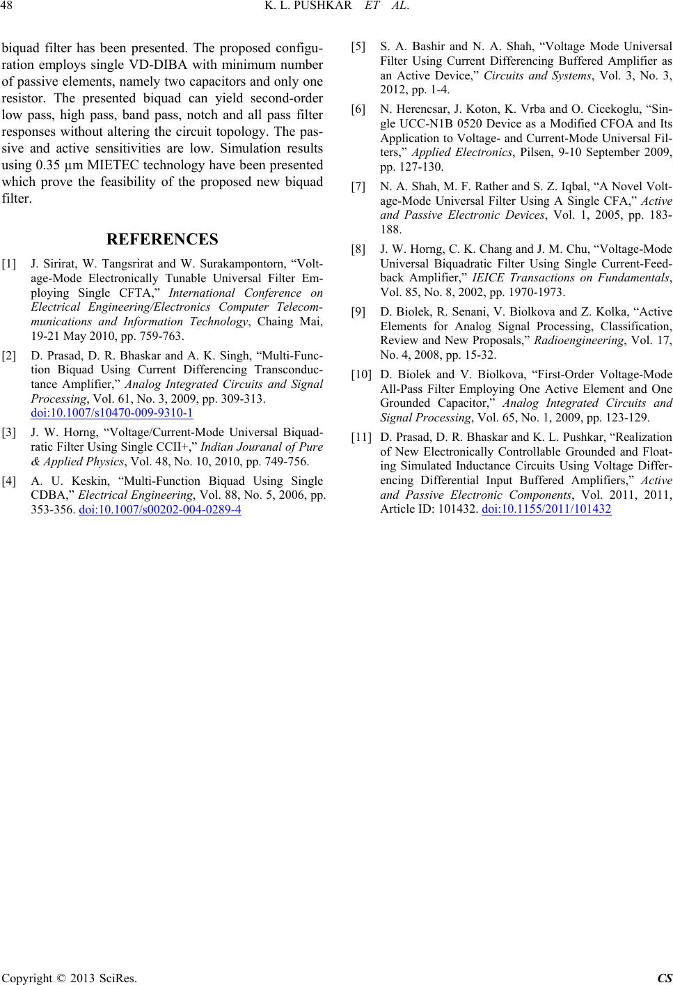 K. L. PUSHKAR ET AL. 48 biquad filter has been presented. The proposed configu- ration employs single VD-DIBA with minimum number of passive elements, namely two capacitors and only one resistor. The presented biquad can yield second-order low pass, high pass, band pass, notch and all pass filter responses without altering the circuit topology. The pas- sive and active sensitivities are low. Simulation results using 0.35 µm MIETEC technology have been presented which prove the feasibility of the proposed new biquad filter. REFERENCES [1] J. Sirirat, W. Tangsrirat and W. Surakampontorn, “Volt- age-Mode Electronically Tunable Universal Filter Em- ploying Single CFTA,” International Conference on Electrical Engineering/Electronics Computer Telecom- munications and Information Technology, Chaing Mai, 19-21 May 2010, pp. 759-763. [2] D. Prasad, D. R. Bhaskar and A. K. Singh, “Multi-Func- tion Biquad Using Current Differencing Transconduc- tance Amplifier,” Analog Integrated Circuits and Signal Processing, Vol. 61, No. 3, 2009, pp. 309-313. doi:10.1007/s10470-009-9310-1 [3] J. W. Horng, “Voltage/Current-Mode Universal Biquad- ratic Filter Using Single CCII+,” Indian Jouranal of Pure & Applied Physics, Vol. 48, No. 10, 2010, pp. 749-756. [4] A. U. Keskin, “Multi-Function Biquad Using Single CDBA,” Electrical Engineering, Vol. 88, No. 5, 2006, pp. 353-356. doi:10.1007/s00202-004-0289-4 [5] S. A. Bashir and N. A. Shah, “Voltage Mode Universal Filter Using Current Differencing Buffered Amplifier as an Active Device,” Circuits and Systems, Vol. 3, No. 3, 2012, pp. 1-4. [6] N. Herencsar, J. Koton, K. Vrba and O. Cicekoglu, “Sin- gle UCC-N1B 0520 Device as a Modified CFOA and Its Application to Voltage- and Current-Mode Universal Fil- ters,” Applied Electronics, Pilsen, 9-10 September 2009, pp. 127-130. [7] N. A. Shah, M. F. Rather and S. Z. Iqbal, “A Novel Volt- age-Mode Universal Filter Using A Single CFA,” Active and Passive Electronic Devices, Vol. 1, 2005, pp. 183- 188. [8] J. W. Horng, C. K. Chang and J. M. Chu, “Voltage-Mode Universal Biquadratic Filter Using Single Current-Feed- back Amplifier,” IEICE Transactions on Fundamentals, Vol. 85, No. 8, 2002, pp. 1970-1973. [9] D. Biolek, R. Senani, V. Biolkova and Z. Kolka, “Active Elements for Analog Signal Processing, Classification, Review and New Proposals,” Radioengineering, Vol. 17, No. 4, 2008, pp. 15-32. [10] D. Biolek and V. Biolkova, “First-Order Voltage-Mode All-Pass Filter Employing One Active Element and One Grounded Capacitor,” Analog Integrated Circuits and Signal Processing, Vol. 65, No. 1, 2009, pp. 123-129. [11] D. Prasad, D. R. Bhaskar and K. L. Pushkar, “Realization of New Electronically Controllable Grounded and Float- ing Simulated Inductance Circuits Using Voltage Differ- encing Differential Input Buffered Amplifiers,” Active and Passive Electronic Components, Vol. 2011, 2011, Article ID: 101432. doi:10.1155/2011/101432 Copyright © 2013 SciRes. CS |