

Paper Menu >>
Journal Menu >>
 Graphene, 2013, 2, 55-59 http://dx.doi.org/10.4236/graphene.2013.21008 Published Online January 2013 (http://www.scirp.org/journal/graphene) Effect of Growth Morphology on the Electronic Structure of Epitaxial Graphene on SiC Michael D. Williams1, Dennis W. Hess2 1Center of Excellence in Microelectronics and Photonics, Department of Physics, Clark Atlanta University, Atlanta, USA 2School of Chemical and Biomolecular Engineering, Georgia Institute of Technology, Atlanta, USA Email: [email protected] Received November 16, 2012; revised December 20, 2012; accepted January 18, 2013 ABSTRACT Ultraviolet photoemission spectroscopy is used to investigate the electronic structure of epitaxial graphene grown by the thermal decomposition of the carbon face of 4H SiC. We find that the growth of the film on the chemical mechanically polished and hydrogen etched surface enhances spectral features in the valence band structure compared to the film grown on an unpolished hydrogen etched substrate. This result is indicative of a more highly ordered surface structure compared to the morphologically rough material and shows that substrate preparation plays an important role in the quality of the film. The work function of the smooth surface film is found to be 0.4 eV higher than that for graphite and 0.1 eV less than for the rough surface growth. Keywords: Graphene; SiC; UPS; Work Function; Electronic Structure 1. Introduction Graphene, the 2-D crystalline form of graphite is the subject of much interest in the fields of optoelectronics, sensors, and hydrogen storage. The high carrier mobility and room temperature ballistic transport of carriers in graphene suggest that this material may be a viable re- placement for copper interconnects in electronic device structures. Most recently, its electronic properties have been shown to be tunable from metallic to semiconduct- ing with hydrogen intercalation [1-3]. Many potential applications for graphene require ordered growth on an insulating substrate. One successful methodology to pro- duce graphene layers has been to thermally decompose SiC in vacuum [4]. More recently larger grain sizes have been reported via thermal decomposition of SiC in an inert gas atmosphere [5,6]. Other reports have explored the processing and growth of epitaxial graphene (EG) layers using biological and chemical functionalization methodologies [7,8]. The latter approach is particularly attractive for sensor and hydrogen storage applications. Due to the critical dependence of graphene properties on the material quality, it is imperative that appropriate characterization methods be employed to assess struc- tural and the associated electronic properties. The 2-D nature of this material makes analysis amenable to tradi- tional surface science techniques. In this work, we use angle integrated ultraviolet photoemission spectroscopy (UPS) to ascertain the effect of the substrate on the per- fection of graphene samples vis-à-vis their electronic valence band structure. Spicer and co-workers in the early 70 s showed conclusively in comparison studies of amorphous Si and Ge samples to corresponding crystal- line material that UPS analysis is a definite indicator of material crystallinity [9]. More recently, a UPS study of few layer graphene grown by chemical vapor deposition on polycrystalline nickel reported a strong correlation to the graphene quality and structure [10]. This study inves- tigates the effects of surface morphology on the elec- tronic structure of EG layers grown by thermal decom- position of the C face of SiC. 2. Experiment The two samples used in this study were grown by the thermal graphitization of the C-face of 4H SiC substrates purchased from Cree, Inc. The substrates were graph- itized by confinement controlled sublimation of Si atoms from SiC in a graphite furnace at the Georgia Institute of Technology [11]. In the confinement controlled process the SiC substrate is encapsulated in a graphite enclosure that maintains a high Si vapor pressure background such that the graphene layer growth proceeds in a near equi- librium fashion. The resulting carbon rich sufaces that result from the Si sublimation nucleate to form an epi- taxial graphen layer. Graphene grown by this methodol- ogy has a much lower occurrence of defects than the ma- terial grown at relatively low growth temperatures and high graphitization rates in the non-equilibium ultra-high vacuum Si sublimation process. The samples were C opyright © 2013 SciRes. Graphene 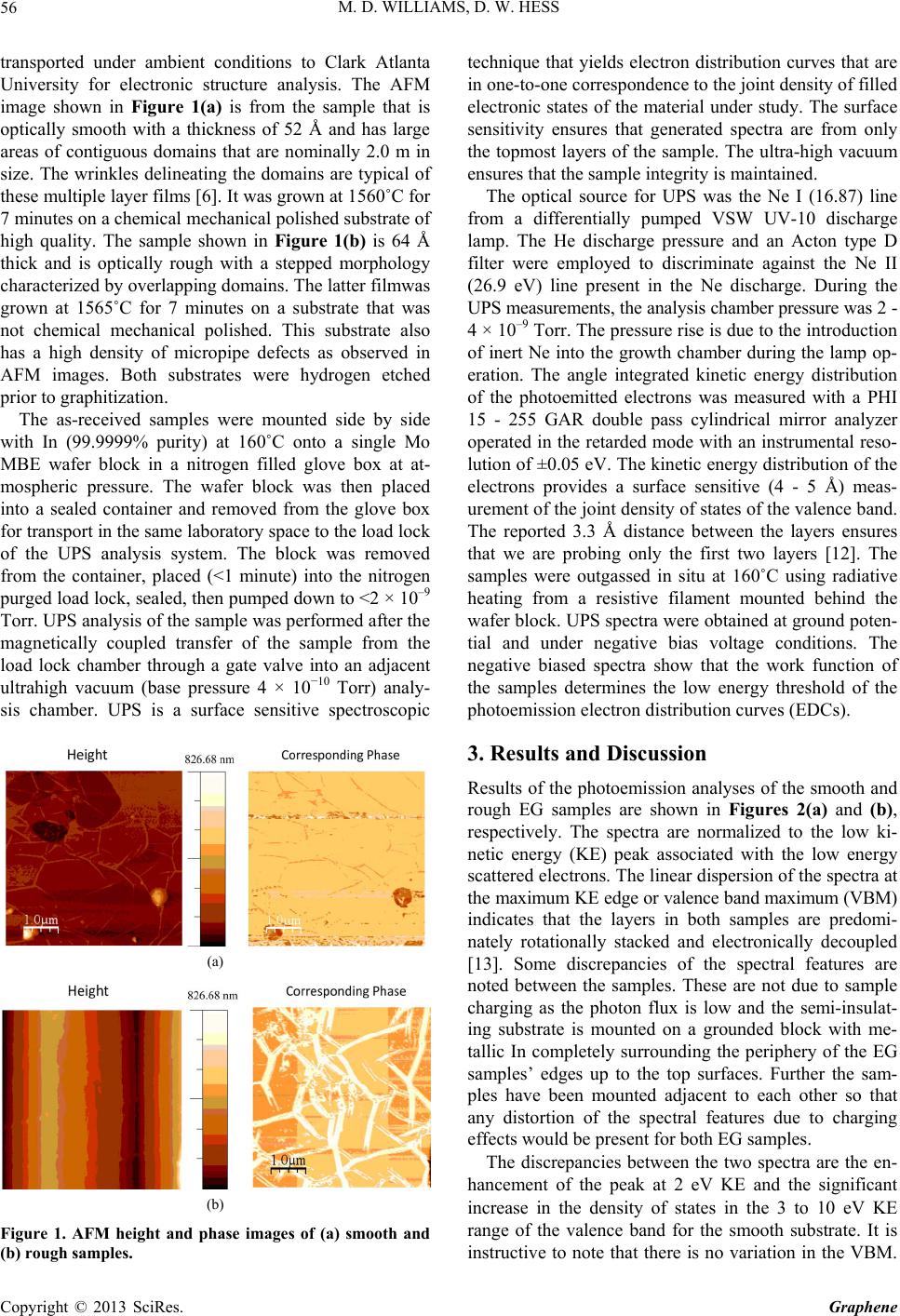 M. D. WILLIAMS, D. W. HESS 56 transported under ambient conditions to Clark Atlanta University for electronic structure analysis. The AFM image shown in Figure 1(a) is from the sample that is optically smooth with a thickness of 52 Å and has large areas of contiguous domains that are nominally 2.0 m in size. The wrinkles delineating the domains are typical of these multiple layer films [6]. It was grown at 1560˚C for 7 minutes on a chemical mechanical polished substrate of high quality. The sample shown in Figure 1(b) is 64 Å thick and is optically rough with a stepped morphology characterized by overlapping domains. The latter filmwas grown at 1565˚C for 7 minutes on a substrate that was not chemical mechanical polished. This substrate also has a high density of micropipe defects as observed in AFM images. Both substrates were hydrogen etched prior to graphitization. The as-received samples were mounted side by side with In (99.9999% purity) at 160˚C onto a single Mo MBE wafer block in a nitrogen filled glove box at at- mospheric pressure. The wafer block was then placed into a sealed container and removed from the glove box for transport in the same laboratory space to the load lock of the UPS analysis system. The block was removed from the container, placed (<1 minute) into the nitrogen purged load lock, sealed, then pumped down to <2 × 10⁻⁹ Torr. UPS analysis of the sample was performed after the magnetically coupled transfer of the sample from the load lock chamber through a gate valve into an adjacent ultrahigh vacuum (base pressure 4 × 10⁻¹⁰ Torr) analy- sis chamber. UPS is a surface sensitive spectroscopic (a) (b) Figure 1. AFM height and phase images of (a) smooth and (b) rough samples. technique that yields electron distribution curves that are in one-to-one correspondence to the joint density of filled electronic states of the material under study. The surface sensitivity ensures that generated spectra are from only the topmost layers of the sample. The ultra-high vacuum ensures that the sample integrity is maintained. The optical source for UPS was the Ne I (16.87) line from a differentially pumped VSW UV-10 discharge lamp. The He discharge pressure and an Acton type D filter were employed to discriminate against the Ne II (26.9 eV) line present in the Ne discharge. During the UPS measurements, the analysis chamber pressure was 2 - 4 × 10⁻⁹ Torr. The pressure rise is due to the introduction of inert Ne into the growth chamber during the lamp op- eration. The angle integrated kinetic energy distribution of the photoemitted electrons was measured with a PHI 15 - 255 GAR double pass cylindrical mirror analyzer operated in the retarded mode with an instrumental reso- lution of ±0.05 eV. The kinetic energy distribution of the electrons provides a surface sensitive (4 - 5 Å) meas- urement of the joint density of states of the valence band. The reported 3.3 Å distance between the layers ensures that we are probing only the first two layers [12]. The samples were outgassed in situ at 160˚C using radiative heating from a resistive filament mounted behind the wafer block. UPS spectra were obtained at ground poten- tial and under negative bias voltage conditions. The negative biased spectra show that the work function of the samples determines the low energy threshold of the photoemission electron distribution curves (EDCs). 3. Results and Discussion Results of the photoemission analyses of the smooth and rough EG samples are shown in Figures 2(a) and (b), respectively. The spectra are normalized to the low ki- netic energy (KE) peak associated with the low energy scattered electrons. The linear dispersion of the spectra at the maximum KE edge or valence band maximum (VBM) indicates that the layers in both samples are predomi- nately rotationally stacked and electronically decoupled [13]. Some discrepancies of the spectral features are noted between the samples. These are not due to sample charging as the photon flux is low and the semi-insulat- ing substrate is mounted on a grounded block with me- tallic In completely surrounding the periphery of the EG samples’ edges up to the top surfaces. Further the sam- ples have been mounted adjacent to each other so that any distortion of the spectral features due to charging effects would be present for both EG samples. The discrepancies between the two spectra are the en- hancement of the peak at 2 eV KE and the significant increase in the density of states in the 3 to 10 eV KE range of the valence band for the smooth substrate. It is instructive to note that there is no variation in the VBM. Copyright © 2013 SciRes. Graphene 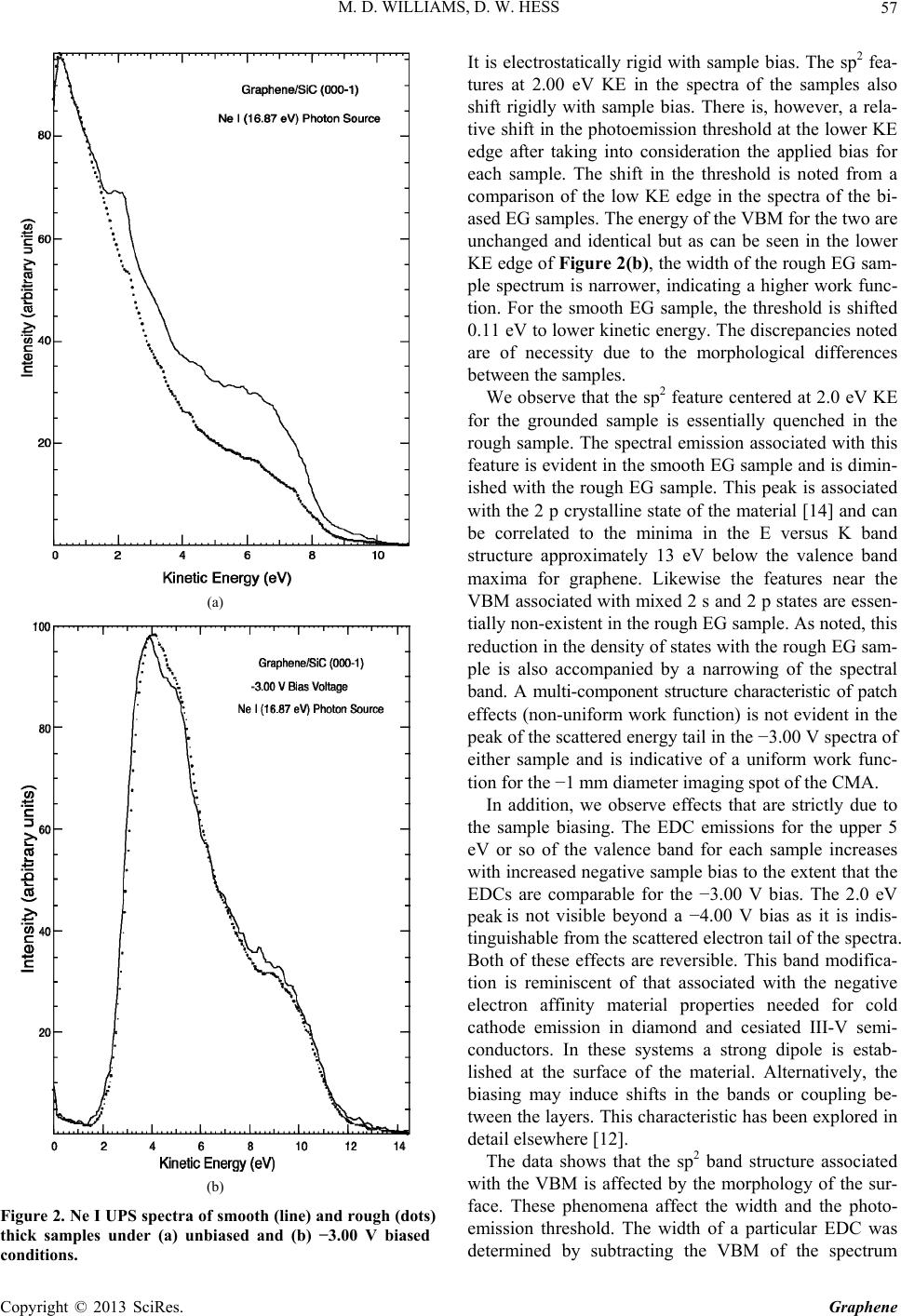 M. D. WILLIAMS, D. W. HESS 57 (a) (b) Figure 2. Ne I UPS spectra of smooth (line) and rough (dots) thick samples under (a) unbiased and (b) −3.00 V biased conditions. It is electrostatically rigid with sample bias. The sp2 fea- tures at 2.00 eV KE in the spectra of the samples also shift rigidly with sample bias. There is, however, a rela- tive shift in the photoemission threshold at the lower KE edge after taking into consideration the applied bias for each sample. The shift in the threshold is noted from a comparison of the low KE edge in the spectra of the bi- ased EG samples. The energy of the VBM for the two are unchanged and identical but as can be seen in the lower KE edge of Figure 2(b), the width of the rough EG sam- ple spectrum is narrower, indicating a higher work func- tion. For the smooth EG sample, the threshold is shifted 0.11 eV to lower kinetic energy. The discrepancies noted are of necessity due to the morphological differences between the samples. We observe that the sp2 feature centered at 2.0 eV KE for the grounded sample is essentially quenched in the rough sample. The spectral emission associated with this feature is evident in the smooth EG sample and is dimin- ished with the rough EG sample. This peak is associated with the 2 p crystalline state of the material [14] and can be correlated to the minima in the E versus K band structure approximately 13 eV below the valence band maxima for graphene. Likewise the features near the VBM associated with mixed 2 s and 2 p states are essen- tially non-existent in the rough EG sample. As noted, this reduction in the density of states with the rough EG sam- ple is also accompanied by a narrowing of the spectral band. A multi-component structure characteristic of patch effects (non-uniform work function) is not evident in the peak of the scattered energy tail in the −3.00 V spectra of either sample and is indicative of a uniform work func- tion for the −1 mm diameter imaging spot of the CMA. In addition, we observe effects that are strictly due to the sample biasing. The EDC emissions for the upper 5 eV or so of the valence band for each sample increases with increased negative sample bias to the extent that the EDCs are comparable for the −3.00 V bias. The 2.0 eV peak is not visible beyond a −4.00 V bias as it is indis- tinguishable from the scattered electron tail of the spectra. Both of these effects are reversible. This band modifica- tion is reminiscent of that associated with the negative electron affinity material properties needed for cold cathode emission in diamond and cesiated III-V semi- conductors. In these systems a strong dipole is estab- lished at the surface of the material. Alternatively, the biasing may induce shifts in the bands or coupling be- tween the layers. This characteristic has been explored in detail elsewhere [12]. The data shows that the sp2 band structure associated with the VBM is affected by the morphology of the sur- face. These phenomena affect the width and the photo- emission threshold. The width of a particular EDC was determined by subtracting the VBM of the spectrum Copyright © 2013 SciRes. Graphene  M. D. WILLIAMS, D. W. HESS 58 from its low energy photoemission threshold. The VBM ismeasured by performing a linear extrapolation of the high kinetic energy edge of the EDC from one half of its maximum intensity to the spectral baseline. The thresh- old of photoemission is determined by the work function of the electrically biased material and is measured by linearly extrapolating the low kinetic energy edge of the EDC from the full width at half maximum of the low energy spectral peak to the spectral baseline. Assuming a constant band gap, g E, the electron affinity, , and the work function, , for a degeneratively doped p-type surface or semi-metal are related by g g EhWE (1) where W is the width of the VB EDC, is measured from the vacuum level (photoemission threshold) to the top of the valence band, is measured from the top of the vacuum level to the bottom of the conduction band, and h is the photon energy. The change in the electron affinity can be written as W . (2) Using a linear extrapolation of the scattering energy tail peaks in Figures 2 (a) and (b) to the baseline we get vacuum levels of 2.2 eV with 3.0 Volt bias and –0.8 eV for the smooth EG grounded sample. Assuming that the material has no band gap, a Fermi level of 13.8 eV and 10.8 eV is obtained by a linear extrapolation of the VB maxima for the respective biases. This implies a total width of 11.6 eV and thus a work function of 5.1 eV for the smooth sample which is about 0.4 eV higher than bulk graphite. The analysis yields a work function of 5.21 eV for the rough EG sample. It should be noted that in situ Auger analysis revealed no contamination of the probed areas of the samples. 4. Summary and Conclusion This work was undertaken to determine if angle inte- grated UPS using common line sources can differentiate between the electrical properties of different epitaxial EG films. We have demonstrated conclusively that UPS can differentiate between the electronic properties of epi- taxial EG films with different growth morphologies. Such is the case for graphene derived from the thermal decomposition of the C-face of SiC and this result is consistent with that reported in the literature for other material systems. The spectral features associated with the crystalline state of the material are significantly quenched when the EG film is graphitized on a rough substrate with a high density of defects present. The re- sults show that the electronic structures are unique for different degrees of order in the studied films and that the ordering is strongly dependent on the substrate prepara- tion. 5. Acknowledgements The authors thanks J. E. Rowe for fruitful discussions and gratefully acknowledges the support of the NSF PREM at Clark Atlanta University, Award # DMR- 0934142, and the NSF MRSEC at the Georgia Institute of Technology, Award # 0820382. We thank Walter de Heer, Claire Berger and Yike Hu of the Georgia Institute of Technology MRSEC for providing the EG samples for this study and Biswasjit Sannigrahi of the NSF CREST at Clark Atlanta University, Award # HRD-0630456, for the AFM images. REFERENCES [1] L F. Shedin, A. K. Geim, S. V. Morozov, E. W. Hill, P. Blake, M. I. Katsnelson and K. S. Novoselov, “Detection of Individual Gas Molecules on Graphene,” Nature Mate- rials, Vol. 6, No. 9, 2007, pp. 652-655. doi:10.1038/nmat1967 [2] X. Wang, L. Zhi and K. Mullen, “Transparent, Conduc- tive Graphene Electrodes for Dye-Synthesized Solar Cells,” Nano Letters, Vol. 8, No. 1, 2008, pp. 323-327. doi:10.1021/nl072838r [3] S. Gilje, S. Han, M. Wang, K. L. Wang and R. B. Kaner, “A Chemical Route to Graphene for Device Applica- tions,” Nano Letters, Vol. 7, No. 11, 2007, pp. 3394-3398. doi:10.1021/nl0717715 [4] W. A. de Heer, C. Berger, X. S. Wu, P. N. First, E. H. Conrad, X. B. Li, T. B. Li, M. Sprinkle, J. Hass, M. L. Sadowski, M. Potemski and G. Martinez, “Epitaxial Gra- phene,” Solid State Communications, Vol. 143, No. 1, 2007, pp. 92-100. doi:10.1016/j.ssc.2007.04.023 [5] K. V. Emtsev, A. Bostwick, K. Horn, J. Jobst, G. L. Kel- logg, L. Ley, J. L. McChesney, T. Ohta, S. A. Reshanov, J. Röhrl, E. Rotenberg, A. K. Schmid, D. Waldmann, H. B. Weber and T. Seyller, “Toward Wafer-Size Graphene Layers by Atmospheric Pressure Graphitization of Silicon Carbide,” Nature Materials , Vol. 8, No. 3, 2009, pp. 203- 207. doi:10.1038/nmat2382 [6] W. Norimatsu, J. Takada and M. Kusunoki, “Formation Mechanism of Graphene Layers on SiC (0001) in a High- Pressure Argon Atmosphere,” Physical Review B, Vol. 84, No. 3, 2011, Article ID: 035424. doi:10.1103/PhysRevB.84.03542 [7] A. Turchanin, A. Beyer, Ch. T. Nottbohm, X. Zhang, R. Stosch, A. Sologubenko, J. Mayer, P. Hinze, T. Weimann, and A. Gölzhäuser, “One Nanometer Thin Carbon Nano- sheets with Tunable Conductivity and Stiffness,” Advanc- ed Materials, Vol. 21, No. 12, 2009, pp. 1233-1237. doi:10.1002/adma.200803078 [8] A. Reina, X. T. Jia, J. Ho, D. Nezich, H. Son, V. Bulovic, M. S. Dresselhaus and J. Kong, “Large Area, Few-Layer Graphene Films on Arbitrary Substrates by Chemical Va- por Deposition,” Nano Letters, Vol. 9, No. 1, 2009, pp. 30-35. doi:10.1021/nl801827v [9] W. E. Spicer, “The Use of Photoemission to Determine the Electronic Structure of Solids,” Journal De Physique Copyright © 2013 SciRes. Graphene  M. D. WILLIAMS, D. W. HESS Copyright © 2013 SciRes. Graphene 59 Colloques, Vol. 34, No. 6, 1973, pp. 19-33. doi:10.1051/jphyscol:1973607 [10] R. J. Koch, A. Reina, J. A. Schaefer and J. Kong, “Am- bient Pressure CVD Grown and Transferred Graphene: STM and UPS Study,” Unpublished, 2009. [11] W. A. de Heer, C. Berger, M. Ruan, M. Sprinkle, X. Li, Y. Hu, B. Zhang, J. Hankinson and E. H. Conrad, “Large Area and Structured Epitaxial Graphene Produced by Confinement Controlled Sublimation of Silicon Carbide,” Proceedings National Academy of Sciences USA, Vol. 108, No. 41, 2011, pp. 16900-16905. doi:10.1073/pnas.1105113108 [12] M. D. Williams, D. K. Samarakoon, D. W. Hess and X.-Q. Wang, “Tunable Bands in Biased Multilayer Epitaxial Graphene,” Nanoscale, Vol. 4, No. 9, 2012, pp. 2962-2967. doi:10.1039/C2NR11991A [13] Z. Chen and X.-Q. Wang, “Stacking-Dependent Optical Spectra and Many-Electron Effects in Bilayer Graphene,” Physical Review B, Vol. 83, No. 8, 2011, Article ID: 081405. doi:10.1103/PhysRevB.83.081405 [14] J. R. Cheliokowsky and M. L. Cohen, “Nonlocal Pseu- dopotential Calculations for the Electronic Structure of Eleven Diamond and Zinc-Blende Semiconductors,” Phy- sical Review B, Vol. 14, No. 2, 1976, pp. 556-582. doi:10.1103/PhysRevB.14.556 |