

Paper Menu >>
Journal Menu >>
 Graphene, 2013, 2, 35-41 http://dx.doi.org/10.4236/graphene.2013.21005 Published Online January 2013 (http://www.scirp.org/journal/graphene) Formation of Interface Bound States on a Graphene-Superconductor Junction in the Presence of Charge Inhomogeneities Pablo Burset1*, William Javier Herrera2, Alfredo Levy Yeyati1 1Departamento de Física Teórica de la Materia Condensada and Instituto Nicolás Cabrera, Universidad Autónoma de Madrid, Madrid, Spain 2Departamento de Física, Universidad Nacional de Colombia, Bogotá, Colombia Email: *[email protected] Received November 12, 2012; revised December 17, 2012; accepted January 14, 2013 ABSTRACT Interface bound states have been theoretically predicted to appear at isolated graphene-superconductor junctions. These states are formed at the interface due to the interplay between virtual Andreev and normal reflections and provide long-range superconducting correlations on the graphene layer. We describe in detail the formation of these states from combining the Dirac equation with the Bogoliubov-de Gennes equations of superconductivity. On the other hand, fluc- tuations of the low-energy charge density in graphene have been confirmed as the dominating type of disorder. For analyzing the effect of disorder on these states we use a microscopic tight-binding model. We show how the formation of these states is robust against the presence of disorder in the form of electron charge inhomogeneities in the graphene layer. We numerically compute the effect of disorder on the interface bound states and on the local density of states of graphene. Keywords: Graphene; Superconducting Hybrid Structures; Andreev Reflection 1. Introduction The peculiar electronic band structure of graphene has been the focus of an intense research activity [1]. In gra- phene, the electronic low-energy properties are governed by a massless relativistic Dirac Hamiltonian which makes the carriers moving in it develop very interesting proper- ties like an electronic spectrum linear with the wave vector and electronic states which are chiral with respect to the pseudospin defined by the two atoms of the crystal unit cell. As a result, graphene exhibits exotic effects like the Klein paradox—perfect transmission through poten- tial barriers [2]. Of particular interest is the case of a graphene layer in contact with a superconducting electrode, where the in- terplay between superconductivity and the relativistic behavior of charge carriers in graphene can be tested [3]. Graphene is not intrinsically a superconductor but it can easily inherit the bulk properties of other materials when in contact with them. Good contacts can be achieved between lithographically defined superconducting elec- trodes and graphene layers [4-7]. In such hybrid devices, a superconducting gap is induced by proximity effect on the graphene region underneath the metallic electrodes; in these conditions, Andreev processes featuring conver- sion of electrons into holes in the normal region and the creation of a Cooper pair in the superconductor take place [8]. In a recent experiment using planar Pb probes a high-quality tunneling spectroscopy has been performed when the Pb was in the superconducting regime [9]. Several theoretical studies of the electronic and trans- port properties of graphene-superconductor hybrid struc- tures have been reported in the recent years. The differ- ential conductance and the spectral properties of gra- phene-superconductor junctions and graphene-based Jo- sephson junctions have been studied within a tight- binding framework and solving the Dirac-Bogoliubov-de Gennes (DBdG) equations under the approximation of neglecting inter-valley scattering [10-19]. The influence of electron-hole inhomogeneities on the Andreev reflec- tion on graphene-superconductor hybrid structures was studied in [20]. The properties of bound states arising from multiple Andreev reflections in a graphene Joseph- son junction have been analyzed in [21,22]. However, the special electronic properties of graphene are such that bound states can be formed even at isolated single junc- tions. The existence of interface bound states (IBS) was demonstrated in [23] for different edge orientations and doping conditions of the graphene layer. In this work we *Corresponding author. C opyright © 2013 SciRes. Graphene 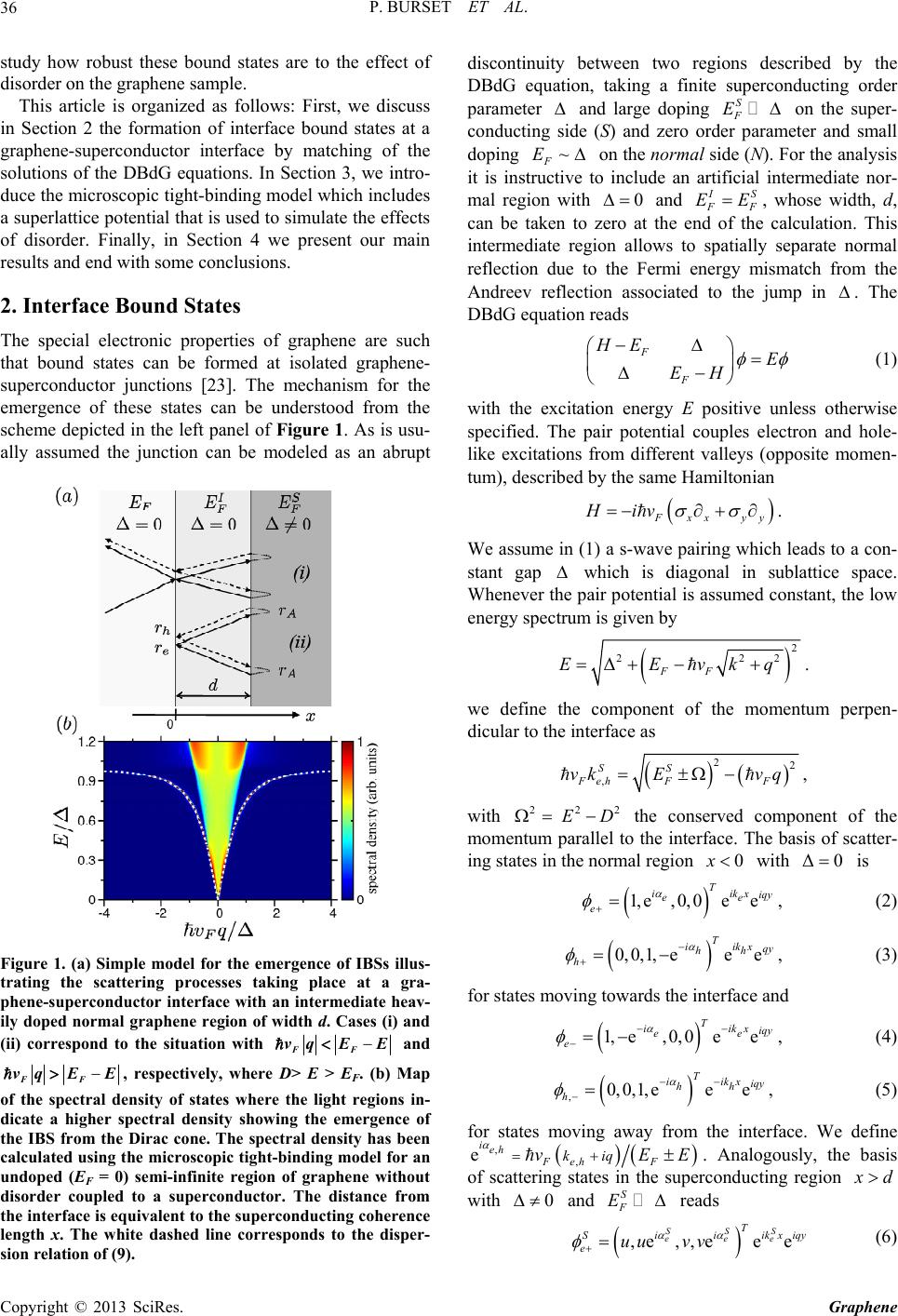 P. BURSET ET AL. 36 study how robust these bound states are to the effect of disorder on the graphene sample. This article is organized as follows: First, we discuss in Section 2 the formation of interface bound states at a graphene-superconductor interface by matching of the solutions of the DBdG equations. In Section 3, we intro- duce the microscopic tight-binding model which includes a superlattice potential that is used to simulate the effects of disorder. Finally, in Section 4 we present our main results and end with some conclusions. 2. Interface Bound States The special electronic properties of graphene are such that bound states can be formed at isolated graphene- superconductor junctions [23]. The mechanism for the emergence of these states can be understood from the scheme depicted in the left panel of Figure 1. As is usu- ally assumed the junction can be modeled as an abrupt Figure 1. (a) Simple model for the emergence of IBSs illus- trating the scattering processes taking place at a gra- phene-superconductor interface with an intermediate heav- ily doped normal graphene region of width d. Cases (i) and (ii) correspond to the situation with FF vq EE and FF v q EE, respectively, where D> E > EF. (b) Map of the spectral density of states where the light regions in- dicate a higher spectral density showing the emergence of the IBS from the Dirac cone. The spectral density has been calculated using the microscopic tight-binding model for an undoped (EF = 0) semi-infinite region of graphene without disorder coupled to a superconductor. The distance from the interface is equivalent to the superconducting coherence length x. The white dashed line corresponds to the disper- sion relation of (9). discontinuity between two regions described by the DBdG equation, taking a finite superconducting order parameter and large doping on the super- conducting side (S) and zero order parameter and small doping S F E F E~ on the normal side (N). For the analysis it is instructive to include an artificial intermediate nor- mal region with 0 and I S F F, whose width, d, can be taken to zero at the end of the calculation. This intermediate region allows to spatially separate normal reflection due to the Fermi energy mismatch from the Andreev reflection associated to the jump in EE . The DBdG equation reads F F HE E EH (1) with the excitation energy E positive unless otherwise specified. The pair potential couples electron and hole- like excitations from different valleys (opposite momen- tum), described by the same Hamiltonian F xx yy Hiv . We assume in (1) a s-wave pairing which leads to a con- stant gap which is diagonal in sublattice space. Whenever the pair potential is assumed constant, the low energy spectrum is given by 2 22 ΔFF EEvkq 2 . we define the component of the momentum perpen- dicular to the interface as 22 , SS Feh FF vk Evq, with 22 ED 2 the conserved component of the momentum parallel to the interface. The basis of scatter- ing states in the normal region with 0xΔ0 is 1, e, 0,0ee T iik iqy ee e x , (2) 0, 0,1,eee T iikx qy hh h , (3) for states moving towards the interface and 1,e, 0, 0ee Tik x iiqy ee e , (4) ,0, 0,1,eee T iikx iqy hh h , (5) for states moving away from the interface. We define , , eieh Feh F kiqvE E. Analogously, the basis of scattering states in the superconducting region x d with 0 and S F E reads ,e ,,eee SSS eee T iiikx Si euu vv qy (6) Copyright © 2013 SciRes. Graphene 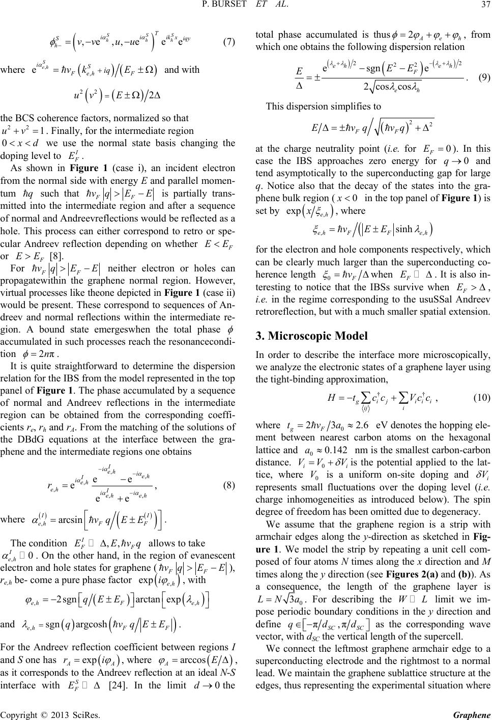 P. BURSET ET AL. 37 ,e,,e ee SSS hhh T iiikx S hvv uu i qy (7) where , , e S eh iS Feh F iqvk E and with 22 2uv E the BCS coherence factors, normalized so that . Finally, for the intermediate region 22 1uv 0 x d we use the normal state basis changing the doping level to I F E. As shown in Figure 1 (case i), an incident electron from the normal side with energy E and parallel momen- tum such that qFF vq EE is partially trans- mitted into the intermediate region and after a sequence of normal and Andreevreflections would be reflected as a hole. This process can either correspond to retro or spe- cular Andreev reflection depending on whether F EE or F EE [8]. For FF vq EE neither electron or holes can propagatewithin the graphene normal region. However, virtual processes like theone depicted in Figure 1 (case ii) would be present. These correspond to sequences of An- dreev and normal reflections within the intermediate re- gion. A bound state emergeswhen the total phase accumulated in such processes reach the resonancecondi- tion 2πn . It is quite straightforward to determine the dispersion relation for the IBS from the model represented in the top panel of Figure 1. The phase accumulated by a sequence of normal and Andreev reflections in the intermediate region can be obtained from the corresponding coeffi- cients re, rh and rA. From the matching of the solutions of the DBdG equations at the interface between the gra- phene and the intermediate regions one obtains ,, , , ,, ee e ee I ieh ieh I ieh eh I ii eh eh r , (8) where ,arcsin II ehF F vqE E . The condition F allows to take ,. On the other hand, in the region of evanescent electron and hole states for graphene ( ,, I F EEvq 0 I eh FF vq EE), re,h be- come a pure phase factor , with ,eh i exp ,, 2sgnarctan exp ehF eh qEE and ,sgn argcosh ehF F qvqE E . For the Andreev reflection coefficient between regions I and S one has A exp A ri , where arccos AE , as it corresponds to the Andreev reflection at an ideal N-S interface with [24]. In the limit the total phase accumulated is thush S F E0d 2 Ae , from which one obtains the following dispersion relation 22 22 gn e s cos eh F eh EE es 2co eh E . (9) This dispersion simplifies to 22 FF Evqvq at the charge neutrality point (i.e. for ). In this case the IBS approaches zero energy for and tend asymptotically to the superconducting gap for large q. Notice also that the decay of the states into the gra- phene bulk region ( 0 F E q0 0 x in the top panel of Figure 1) is set by , exp eh x , where ,, sinh eh FFeh vEE for the electron and hole components respectively, which can be clearly much larger than the superconducting co- herence length 0F v when . It is also in- teresting to notice that the IBSs survive when , i.e. in the regime corresponding to the usuSSal Andreev retroreflection, but with a much smaller spatial extension. F E F E 3. Microscopic Model In order to describe the interface more microscopically, we analyze the electronic states of a graphene layer using the tight-binding approximation, †† g ij iii ij i H tcc Vcc , (10) where 0 232.6 gF tva eV denotes the hopping ele- ment between nearest carbon atoms on the hexagonal lattice and 00.142 a nm is the smallest carbon-carbon distance. 0 i VV V i is the potential applied to the lat- tice, where 0 V is a uniform on-site doping and i V represents small fluctuations over the doping level (i.e. charge inhomogeneities as introduced below). The spin degree of freedom has been omitted due to degeneracy. We assume that the graphene region is a strip with armchair edges along the y-direction as sketched in Fig- ure 1. We model the strip by repeating a unit cell com- posed of four atoms N times along the x direction and M times along the y direction (see Figures 2(a) and (b)). As a consequence, the length of the graphene layer is 0 3LNa. For describing the limit we im- pose periodic boundary conditions in the y direction and define WL π,π qdd SCSC as the corresponding wave vector, with dSC the vertical length of the supercell. We connect the leftmost graphene armchair edge to a superconducting electrode and the rightmost to a normal lead. We maintain the graphene sublattice structure at the edges, thus representing the experimental situation where Copyright © 2013 SciRes. Graphene 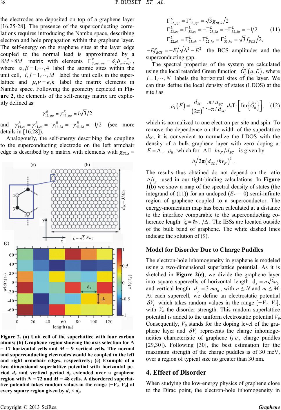 P. BURSET ET AL. 38 the electrodes are deposited on top of a graphene layer [16,25-28]. The presence of the superconducting corre- lations requires introducing the Nambu space, describing electron and hole propagation within the graphene layer. The self-energy on the graphene sites at the layer edge coupled to the normal lead is approximated by a 88 M M matrix with elements ,, R R ijij v , where ,1,,4 ,1,ij , label the atomic sites within the unit cell, label the unit cells in the super- lattice and ,M ,eh label the matrix elements in Nambu space. Following the geometry depicted in Fig- ure 2, the elements of the self-energy matrix are explic- itly defined as 11, 44,32 RR i and 14, 41,14,41,12 RR RR ee eehhhh (see more details in [16,28]). Analogously, the self-energy describing the coupling to the superconducting electrode on the left armchair edge is described by a matrix with elements with gBCS = Figure 2. (a) Unit cell of the superlattice with four carbon atoms; (b) Graphene region showing the axis selection for N = 17 horizontal cells and M = 9 vertical cells. The normal and superconducting electrodes would be coupled to the left and right armchair edges, respectively; (c) Example of a two dimensional superlattice potential with horizontal pe- riod dx and vertical period dy extended over a graphene region with N = 72 and M = 48 cells. A disordered superlat- tice potential takes random values in the range [−Vd, Vd] at every square region given by dx × dy. 22, 33, 23, 33,23,32, 22,33, 22,33, 32 12 32 LL BCS LL LL ee eehhhh LLLL ehehheheBCS g f , (11) 2 BCS Ef EE 2 the BCS amplitudes and the superconducting gap. The spectral properties of the system are calculated using the local retarded Green function , where ˆ, r ii GqE 1, , iN labels the horizontal sites of the layer. We can thus define the local density of states (LDOS) at the site i as 2 π/ˆ Tr Im π/ 2π r SC SC q ii SC dd Ed d i G , (12) which is normalized to one electron per site and spin. To remove the dependence on the width of the superlattice dSC, it is convenient to normalize the LDOS with the density of a bulk graphene layer with zero doping at E, 0 , which for F SC vd is given by 2 2π SC F dv. The results thus obtained do not depend on the ratio g t used in our tight-binding calculations. In Figure 1(b) we show a map of the spectral density of states (the integrand of (11)) for an undoped (EF = 0) semi-infinite region of graphene coupled to a superconductor. The energy-momentum map has been calculated at a distance to the interface comparable to the superconducting co- herence length F v. The IBSs are located outside of the bulk band of graphene. The white dashed lines indicate the solution of (9). Model for Disorder Due to Charge Puddles The electron-hole inhomogeneity in graphene is modeled using a two-dimensional superlattice potential. As it is sketched in Figure 2(c), we divide the graphene layer into square supercells of horizontal length 0 d3 xna and vertical length 0 3 y dma, with n ≤ N and m ≤ M. At each supercell, we define an electrostatic potential i V which takes random values in the range [−Vd, Vd], with Vd the disorder strength. This random superlattice potential is added to the uniform electrostatic potential V0. Consequently, V0 stands for the doping level of the gra- phene layer and i V represents the charge inhomoge- neities characteristic of graphene (i.e., charge puddles [29,30]). Following [30], the best estimation for the maximum strength of the charge puddles is of 30 meV, over a region of typical size no greater than 30 nm. 4. Effect of Disorder When studying the low-energy physics of graphene close to the Dirac point, the electron-hole inhomogeneity in Copyright © 2013 SciRes. Graphene  P. BURSET ET AL. 39 graphene (i.e., charge puddles [29,30]) is a type of charge disorder that has to be taken into account. The results presented in Figure 1(b) correspond to a semi-infinite layer of pristine graphene connected to a superconductor. A more realistic model should include size effects such as a graphene layer with a finite length, and the possibility of electron-density inhomogeneities. Although the effect of having a finite length in the nor- mal region can be treated within both the continuous and the TB models, the latter is more suitable to explore the effect of disorder. The results for a graphene layer of horizontal length 0 3800La with armchair edges coupled to a su- perconductor are presented in Figure 3. Figure 3(a) has been calculated with the strength of the disorder potential set to zero. The results for the LDOS (right panel) are similar to the undoped case presented in [16]: a clear peak at , which rapidly decays inside the normal region after a few times the superconducting coherence length ξ. The finite length of the graphene layer is mani- fested by the appearance of energy bands close to the gap edge. The spectral density of states is plotted in the left E Figure 3. LDOS for a graphene layer of length L = 197 nm (800 armchair cells) coupled to a superconductor on an armchair edge calculated within the tight-binding model. For the simulation, the superconducting gap has been cho- sen to be D = 0.005 tg. (a) The results for the case without disorder. On the left, the spectral density of states, calcu- lated at a distance from the interface comparable to the superconducting coherence length x, in a color map where dark blue is the absence of states. On the right, the LDOS as a function of the energy and the distance to the inter- face; (b) The same as before with the introduction of a ran- dom superlattice potential of strength Vd = 0.01 tg, with spa- tial periods nm. 10 xy dd panel, calculated at a distance ξ from the interface. The IBS is clearly distinguishable outside of the Dirac cone (dark red in the color plot, the dark blue corresponds to the absence of spectral density). The finite armchair layer considered now presents a gap in the energy of the nor- mal state. The Dirac cone is not uniform but is formed by discrete energy levels (light blue areas in the color plot) due to the finite size of the layer. When the disorder is taken into account (Figure 3(b)), the peak at the edge of the gap remains unaltered and the decay is comparable to the non-disordered case (right panel). The weight of the states below the gap becomes more important in the spectral density, as it is shown in the left panel. The energy levels are deformed and ac- quire a bigger weight in the spectral density (light blue in the color plot). For this strength of the disorder, the envelope of the LDOS is still comparable to the non-disordered case, but small fluctuations appear. The main effect of disorder can be seen as an effective doping, which does not alter deeply the LDOS. In Figure 4 we show the LDOS cal- culated at a distance from the interface 6 , where the IBS has completely decayed. The solid red line corre- sponds to the case where the disorder strength is set to zero. The LDOS presents a soft modulation and is sym- metric with respect to the energy—as corresponds to an undoped case. The introduction of disorder breaks this electron-hole symmetry and clearly affects the modu- lation of the LDOS (blue dashed line). The strength of the random superlattice potential used in these simulations is 0.01 2.7 dg Vt meV, which is comparable to the greatest estimation for the measured strength of the charge inhomogeneities in graphene [30]. The periodicity of the superlattice potential is 10 xy dd nm, which is slightly smaller than the typi- Figure 4. LDOS with the same parameters as in Figure 3 calculated at a distance 6× from the interface for the case without disorder (red solid line) and with disorder strength Vd = 0.01 tg (blue dashed line). Copyright © 2013 SciRes. Graphene  P. BURSET ET AL. 40 cal length of a charge puddle in graphene, with an aver- age size of 30 nm. In spite of this, the chosen values are close enough to assume that a bigger period for the su- perlattice potential would not affect considerably the LDOS profiles. In conclusion, we have shown that interface bound states appear at isolated graphene-superconductor junc- tions. The presence of charge inhomogeneities in the normal region induces strong fluctuations in the LDOS profile and breaks the electron-hole symmetry of the LDOS. However, the IBS modifies more intensely the LDOS and thus this electron-hole symmetry cannot be appreciated at a distance from the interface comparable to 2 - 3 ξ. For a longer distance, the IBS have decayed and the effect of the disorder is clearly shown in the LDOS. The formation of IBSs and their effect on the profile of the LDOS is robust against a disorder strength comparable to the measured strength of the charge pud- dles in graphene. 5. Acknowledgements This work was supported by MICINN-Spain via grant FIS2008-04209 and EU project SE2ND (PB and ALY) and COLCIENCIAS, project 110152128235 (WJH). REFERENCES [1] S. Das Sarma, S. Adam, E. H. Hwang and E. Rossi, “Electronic Transport in Two-Dimensional Graphene,” Reviews of Modern Physics, Vol. 83, No. 2, 2011, pp. 407-470. doi:10.1103/RevModPhys.83.407 [2] M. I. Katsnelson, K. S. Novoselov and A. K. Geim, “Chiral Tunnelling and the Klein Paradox in Graphene,” Nature Physics, Vol. 2, 2006, p. 620. doi:10.1038/nphys384 [3] C. W. J. Beenakker, “Colloquium: Andreev Reflection and Klein Tunneling in Graphene,” Reviews of Modern Physics, Vol. 80, No. 4, 2008, pp. 1337-1354. doi:10.1103/RevModPhys.80.1337 [4] H. B. Heersche, P. Jarillo-Herrero, J. B. Oostinga, L. M. K. Vandersypen and A. F. Morpurgo, “Bipolar Supercur- rent in Graphene,” Nature (London), Vol. 446, 2007, p. 56. doi:10.1038/nature05555 [5] F. Miao, S. Wijeratne, Y. Zhang, U. C. Coskun, W. Bao and C. N. Lau, “Phase-Coherent Transport in Graphene Quantum Billiards,” Science, Vol. 317, No. 5844, 2007, pp. 1530-1533. doi:10.1126/science.1144359 [6] A. Shailos, W. Nativel, A. Kasumov, C. Collet, M. Fer- rier, S. Guèron, R. Deblock and H. Bouchiat, “Proximity Effect and Multiple Andreev Reflections in Few-Layer Graphene,” EPL (Europhysics Letters), Vol. 79, No. 5, 2007, p. 57008. doi:10.1209/0295-5075/79/57008 [7] X. Du, I. Skachko and E. Y. Andrei, “Josephson Current and Multiple Andreev Reflections in Graphene SNS Junc- tions,” Physical Review B, Vol. 77, No. 18, 2008, Article ID: 184507. doi:10.1103/PhysRevB.77.184507 [8] C. W. J. Beenakker, “Specular Andreev Reflection in Gra- phene,” Physical Review Letters, Vol. 97, No. 6, 2006, Article ID: 067007. doi:10.1103/PhysRevLett.97.067007 [9] Y. Li and N. Mason, “Tunneling Spectroscopy of Gra- phene Using Planar Pb Probes,” 2012. arXiv:1210.4987 [cond-mat.meshall]. [10] C. W. J. Beenakker, R. A. Sepkhanov, A. R. Akhmerov and J. Tworzydlo, “Quantum Goos-Hänchen Effect in Graphene,” Physical Review Letters, Vol. 102, No. 14, 2009, Article ID: 146804. doi:10.1103/PhysRevLett.102.146804 [11] S. Bhattacharjee and K. Sengupta, “Tunneling Conduc- tance of Graphene NIS Junctions,” Physical Review Let- ters, Vol. 97, No. 21, 2006, Article ID: 217001. doi:10.1103/PhysRevLett.97.217001 [12] A. R. Akhmerov and C. W. J. Beenakker, “Pseudodiffu- sive Conduction at the Dirac Point of a Normal-Supercon- Ductor Junction in Graphene,” Physical Review B, Vol. 75, No. 4, 2007, Article ID: 045426. doi:10.1103/PhysRevB.75.045426 [13] G. Tkachov, “Fine Structure of the Local Pseudogap and Fano Effect for Superconducting Electrons near a Zigzag Graphene Edge,” Physical Review B, Vol. 76, No. 23, 2007, Article ID: 235409. doi:10.1103/PhysRevB.76.235409 [14] J. Linder and A. Sudbø, “Dirac Fermions and Conduc- tance Oscillations in $s$- and $d$-Wave Superconductor- Graphene Junctions,” Physical Review Letters, Vol. 99, No. 14, 2007, Article ID: 147001. doi:10.1103/PhysRevLett.99.147001 [15] J. Linder and A. Sudbø, “Tunneling Conductance in $s$- and $d$-Wave Superconductor-Graphene Junctions: Ex- tended Blonder-Tinkham-Klapwijk Formalism,” Physical Review B, Vol. 77, No. 14, 2008, Article ID: 064507. doi:10.1103/PhysRevB.77.064507 [16] P. Burset, A. L. Yeyati and A. Martín-Rodero, “Micro- scopic Theory of the Proximity Effect in Superconductor- Graphene Nanostructures,” Physical Review B, Vol. 77, No. 20, 2008, Article ID: 205425. doi:10.1103/PhysRevB.77.205425 [17] J. Cserti, I. Hagymási and A. Kormányos, “Graphene Andreev Billiards,” Physical Review B, Vol. 80, No. 7, 2009, Article ID: 073404. doi:10.1103/PhysRevB.80.073404 [18] D. Rainis, F. Taddei, F. Dolcini, M. Polini and R. Fazio, “Andreev Reflection in Graphene Nanoribbons,” Physical Review B, Vol. 79, No. 11, 2009, Article ID: 115131. doi:10.1103/PhysRevB.79.115131 [19] Q.-F. Sun and X. C. Xie, “Quantum Transport through a Graphene Nanoribbon-Superconductor Junction,” Journal of Physics: Condensed Matter Vol. 21, No. 34, 2009, Ar- ticle ID: 344204. doi:10.1088/0953-8984/21/34/344204 [20] S.-G. Cheng, H. Zhang and Q.-F. Sun, “Effect of Elec- tron-Hole Inhomogeneity on Specular Andreev Reflection and Andreev Retroreflection in a Graphene-Supercon- ductor Hybrid System,” Physical Review B, Vol. 83, No. 23, 2011, Article ID: 235403. Copyright © 2013 SciRes. Graphene  P. BURSET ET AL. Copyright © 2013 SciRes. Graphene 41 doi:10.1103/PhysRevB.83.235403 [21] M. Titov, A. Ossipov and C. W. J. Beenakker, “Excita- tion Gap of a Graphene Channel with Superconducting Boundaries,” Physical Review B, Vol. 75, No. 4, 2007, Article ID: 045417. doi:10.1103/PhysRevB.75.045417 [22] D. L. Bergman and K. Le Hur, “Near-Zero Modes in Condensate Phases of the Dirac Theory on the Honey- comb Lattice,” Physical Review B, Vol. 79, No. 18, 2009, Article ID: 184520. doi:10.1103/PhysRevB.79.184520 [23] P. Burset, W. Herrera and A. L. Yeyati, “Proximity-In- duced Interface Bound States in Superconductor-Gra- phene Junctions,” Physical Review B, Vol. 80, No. 4, 2009, Article ID: 041402. doi:10.1103/PhysRevB.80.041402 [24] G. E. Blonder, M. Tinkham and T. M. Klapwijk, “Transi- tion from Metallic to Tunneling Regimes in Supercon- ducting Microconstrictions: Excess Current, Charge Im- balance, and Supercurrent Conversion,” Physical Review B, Vol. 25, No. 7, 1982, pp. 4515-4532. doi:10.1103/PhysRevB.25.4515 [25] H. Schomerus, “Effective Contact Model for Transport through Weakly-Doped Graphene,” Physical Review B, Vol. 76, No. 4, 2007, Article ID: 045433. doi:10.1103/PhysRevB.76.045433 [26] Y. M. Blanter and I. Martin, “Transport through Normal- Metal Graphene Contacts,” Physical Review B, Vol. 76, No. 15, 2007, Article ID: 155433. doi:10.1103/PhysRevB.76.155433 [27] L. Brey and H. A. Fertig, “Magnetoresistance of Gra- phene-Based Spin Valves,” Physical Review B, Vol. 76, No. 20, 2007, Article ID: 205435. doi:10.1103/PhysRevB.76.205435 [28] P. Burset, A. L. Yeyati, L. Brey and H. A. Fertig, “Tran- sport in Superlattices on Single-Layer Graphene,” Physi- cal Review B, Vol. 83, No. 19, 2011, Article ID: 195434. doi:10.1103/PhysRevB.83.195434 [29] J. Martin, N. Akerman, G. Ulbricht, T. Lohmann, J. H. Smet, K. Von Klitzing and A. Yacoby, “Observation of Electron-Hole Puddles in Graphene Using a Scanning Single-Electron Transistor,” Nature Physics, Vol. 4, No. 2, 2008, pp. 144-148. doi:10.1038/nphys781 [30] Y. Zhang, V. W. Brar, C. Girit, A. Zettl and M. F. Crom- mie, “Origin of Spatial Charge Inhomogeneity in Gra- phene,” Nature Physics, Vol. 5, No. 10, 2009, pp. 722- 726. doi:10.1038/nphys1365 |