

Paper Menu >>
Journal Menu >>
 Graphene, 2013, 2, 13-17 http://dx.doi.org/10.4236/graphene.2013.21003 Published Online January 2013 (http://www.scirp.org/journal/graphene) Flexible Graphene Devices with an Embedded Back-Gate Jasper van Veen, Andres Castellanos-Gomez*, Herre S. J. van der Zant, Gary A. Steele* Kavli Institute of Nanoscience, Delft University of Technology, Delft, The Netherlands Email: *[email protected] , *[email protected] Received November 8, 2012; revised December 11, 2012; accepted January 9, 2013 ABSTRACT We show the fabrication of flexible graphene devices with an embedded back-gate. The resistance of these devices can be tuned by changing the strain through the bending of the substrate. These devices can be useful for applications re- quiring a flexible graphene-based field effect transistor in where the graphene channel is not covered (such as biological or chemical sensors and photo-detectors). Keywords: Graphene Device; Flexible Electronics; Back-Gate; Strain Engineering 1. Introduction Graphene is a two-dimensional material made of carbon atoms arranged in a honeycomb lattice [1]. Since its iso- lation by mechanical exfoliation, a great number of ex- perimental and theoretical works have been carried out to deeply study this novel material. Due to this effort a lot of interesting properties and applications have been dis- covered [2], such as the experimental observation of the quantum Hall effect even at room temperature [3] and the possibility to use graphene as a sensor of individual molecules [4]. Additionally, due to its ambipolar field effect graphene can be used as the channel material for a Field Effect Transistor (FET) [5]. Graphene FETs could have small channel lengths and high mobilities of the charge carriers. These properties make graphene FETs advantageous for high-speed applications [6-8]. Together with its electronic properties, graphene also show exceptional mechanical properties that make this material very promising for flexible electronic applica- tions [9-12]. Flexible graphene-based devices will allow one to modify the electronic properties of the device by simply bending it [13-15]. A similar strategy, referred as strain engineering has been successfully employed to modify the electronic pro- perties of traditional semiconducting materials. In con- ventional strain engineering, however, the amount of strain is fixed and it is controlled by epitaxially growing a certain semiconductor on top of an acceptor substrate which has a different lattice parameter [16]. It could be an advantage to be able to have control over the amount of strain and therewith the electronic properties of a ma- terial. However, most of fabricated flexible graphene-devices lack of a gate electrode which limits its usefulness [17, 18]. In fact, flexible graphene FETs with a local top gate has been recently reported [19,20] and flexible devices with a back-gate have not been reported yet. A flexible back-gated graphene FET could be advantageous in many applications requiring the graphene surface to be uncovered such as graphene based chemical sensors or graphene based photo-detectors. In this paper we present a method to fabricate gra- phene flexible FETs with an embedded back-gate. Subse- quently, basic measurements of the strain dependent electronic properties of graphene are presented. 2. Sample Fabrication 2.1. Flexible Substrates The flexible graphene devices are fabricated onto a commercial 500 µm thick polyimide substrate (Cirlex®). Prior to the fabrication, the substrates have been polished with Brasso® polishing solution to reduce the roughness as much as possible. After that, two fabrication steps are followed. In the first step a 100 nm thick layer of alumi- num, which will be used as the back-gate, is evaporated using electron beam evaporation. A shadow mask can be used to pattern the back-gate in a strip geometry. In the second step, a ~5 µm layer of polyimide is spin coated and cured in vacuum to act as a dielectric layer between the gate and the graphene. Figure 1 shows a schematic representation cross-section of the final flexible sub- strates. 2.2. Graphene Transfer After the preparation of the flexible substrate with the embedded gate, graphene is transfer to the substrate sur- face. This process is schematically depicted in Figure 2 *Corresponding authors. C opyright © 2013 SciRes. Graphene 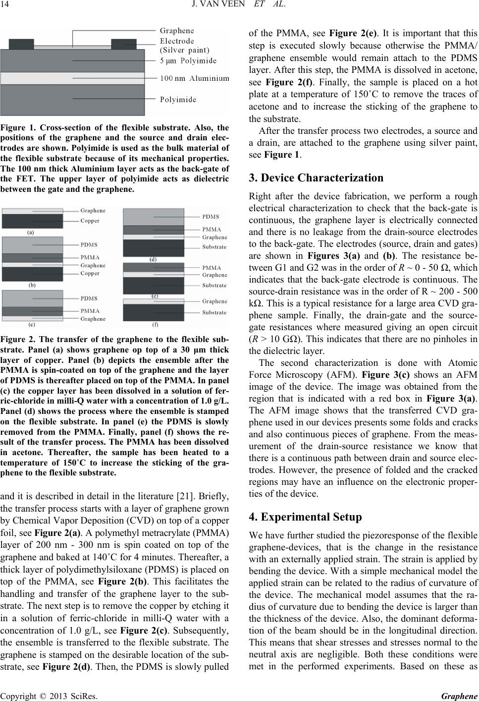 J. VAN VEEN ET AL. 14 Figure 1. Cross-section of the flexible substrate. Also, the positions of the graphene and the source and drain elec- trodes are shown. Polyimide is used as the bulk material of the flexible substrate because of its mechanical properties. The 100 nm thick Aluminium layer acts as the back-gate of the FET. The upper layer of polyimide acts as dielectric between the gate and the graphene. Figure 2. The transfer of the graphene to the flexible sub- strate. Panel (a) shows graphene op top of a 30 μm thick layer of copper. Panel (b) depicts the ensemble after the PMMA is spin-coated on top of the graphene and the layer of PDMS is thereafter placed on top of the PMMA. In panel (c) the copper layer has been dissolved in a solution of fer- ric-chloride in milli-Q water with a concentration of 1.0 g/L. Panel (d) shows the process where the ensemble is stamped on the flexible substrate. In panel (e) the PDMS is slowly removed from the PMMA. Finally, panel (f) shows the re- sult of the transfer process. The PMMA has been dissolved in acetone. Thereafter, the sample has been heated to a temperature of 150˚C to increase the sticking of the gra- phene to the flexible substrate. and it is described in detail in the literature [21]. Briefly, the transfer process starts with a layer of graphene grown by Chemical Vapor Deposition (CVD) on top of a copper foil, see Figure 2(a). A polymethyl metracrylate (PMMA) layer of 200 nm - 300 nm is spin coated on top of the graphene and baked at 140˚C for 4 minutes. Thereafter, a thick layer of polydimethylsiloxane (PDMS) is placed on top of the PMMA, see Figure 2(b). This facilitates the handling and transfer of the graphene layer to the sub- strate. The next step is to remove the copper by etching it in a solution of ferric-chloride in milli-Q water with a concentration of 1.0 g/L, see Figure 2(c). Subsequently, the ensemble is transferred to the flexible substrate. The graphene is stamped on the desirable location of the sub- strate, see Figure 2(d). Then, the PDMS is slowly pulled of the PMMA, see Figure 2(e). It is important that this step is executed slowly because otherwise the PMMA/ graphene ensemble would remain attach to the PDMS layer. After this step, the PMMA is dissolved in acetone, see Figure 2(f). Finally, the sample is placed on a hot plate at a temperature of 150˚C to remove the traces of acetone and to increase the sticking of the graphene to the substrate. After the transfer process two electrodes, a source and a drain, are attached to the graphene using silver paint, see Figure 1. 3. Device Characterization Right after the device fabrication, we perform a rough electrical characterization to check that the back-gate is continuous, the graphene layer is electrically connected and there is no leakage from the drain-source electrodes to the back-gate. The electrodes (source, drain and gates) are shown in Figures 3(a) and (b). The resistance be- tween G1 and G2 was in the order of R ~ 0 - 50 Ω, which indicates that the back-gate electrode is continuous. The source-drain resistance was in the order of R ~ 200 - 500 kΩ. This is a typical resistance for a large area CVD gra- phene sample. Finally, the drain-gate and the source- gate resistances where measured giving an open circuit (R > 10 GΩ). This indicates that there are no pinholes in the dielectric layer. The second characterization is done with Atomic Force Microscopy (AFM). Figure 3(c) shows an AFM image of the device. The image was obtained from the region that is indicated with a red box in Figure 3(a). The AFM image shows that the transferred CVD gra- phene used in our devices presents some folds and cracks and also continuous pieces of graphene. From the meas- urement of the drain-source resistance we know that there is a continuous path between drain and source elec- trodes. However, the presence of folded and the cracked regions may have an influence on the electronic proper- ties of the device. 4. Experimental Setup We have further studied the piezoresponse of the flexible graphene-devices, that is the change in the resistance with an externally applied strain. The strain is applied by bending the device. With a simple mechanical model the applied strain can be related to the radius of curvature of the device. The mechanical model assumes that the ra- dius of curvature due to bending the device is larger than the thickness of the device. Also, the dominant deforma- tion of the beam should be in the longitudinal direction. This means that shear stresses and stresses normal to the neutral axis are negligible. Both these conditions were met in the performed expeiments. Based on these as r Copyright © 2013 SciRes. Graphene 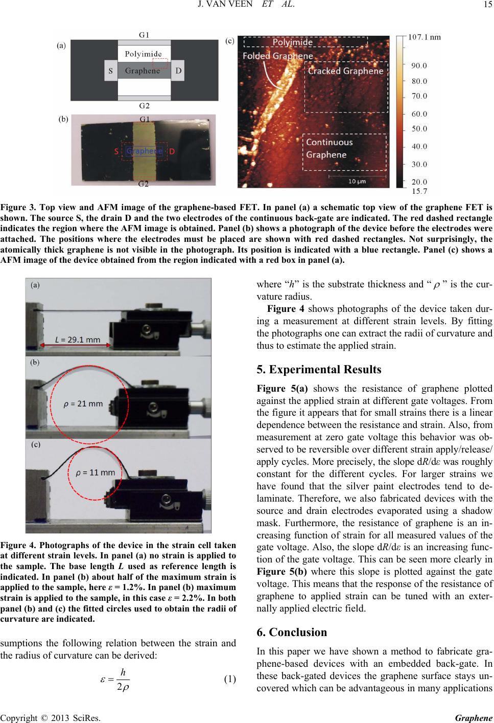 J. VAN VEEN ET AL. Copyright © 2013 SciRes. Graphene 15 Figure 3. Top view and AFM image of the graphene-based FET. In panel (a) a schematic top view of the graphene FET is shown. The source S, the drain D and the two electrodes of the continuous back-gate are indicated. The red dashed rectangle indicates the region where the AFM image is obtained. Panel (b) shows a photograph of the device before the electrodes were attached. The positions where the electrodes must be placed are shown with red dashed rectangles. Not surprisingly, the atomically thick graphene is not visible in the photograph. Its position is indicated with a blue rectangle. Panel (c) shows a AFM image of the device obtained from the region indicated with a red box in panel (a). where “h” is the substrate thickness and “ ” is the cur- vature radius. Figure 4 shows photographs of the device taken dur- ing a measurement at different strain levels. By fitting the photographs one can extract the radii of curvature and thus to estimate the applied strain. 5. Experimental Results Figure 5(a) shows the resistance of graphene plotted against the applied strain at different gate voltages. From the figure it appears that for small strains there is a linear dependence between the resistance and strain. Also, from measurement at zero gate voltage this behavior was ob- served to be reversible over different strain apply/release/ apply cycles. More precisely, the slope dR/dε was roughly constant for the different cycles. For larger strains we have found that the silver paint electrodes tend to de- laminate. Therefore, we also fabricated devices with the source and drain electrodes evaporated using a shadow mask. Furthermore, the resistance of graphene is an in- creasing function of strain for all measured values of the gate voltage. Also, the slope dR/dε is an increasing func- tion of the gate voltage. This can be seen more clearly in Figure 5(b) where this slope is plotted against the gate voltage. This means that the response of the resistance of graphene to applied strain can be tuned with an exter- nally applied electric field. Figure 4. Photographs of the device in the strain cell taken at different strain levels. In panel (a) no strain is applied to the sample. The base length L used as reference length is indicated. In panel (b) about half of the maximum strain is applied to the sample, here ε = 1.2%. In panel (b) maximum strain is applied to the sample, in this case ε = 2.2%. In both panel (b) and (c) the fitted circles used to obtain the radii of curvature are indicated. 6. Conclusion sumptions the following relation between the strain and the radius of curvature can be derived: In this paper we have shown a method to fabricate gra- phene-based devices with an embedded back-gate. In these back-gated devices the graphene surface stays un- covered which can be advantageous in many applications 2 h (1) 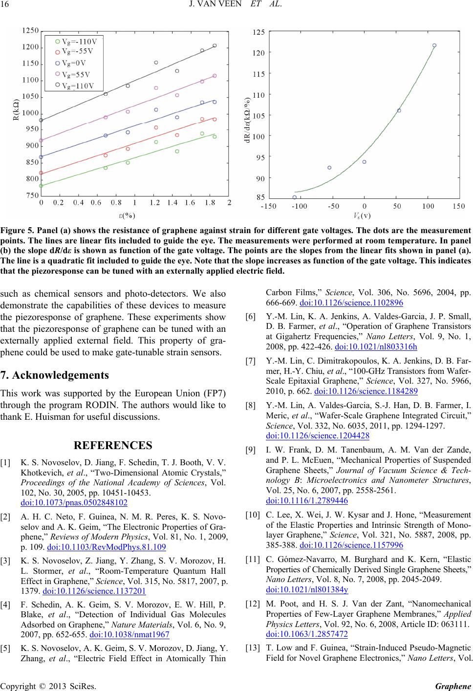 J. VAN VEEN ET AL. 16 Figure 5. Panel (a) shows the resistance of graphene against strain for different gate voltages. The dots are the measurement points. The lines are linear fits included to guide the eye. The measurements were performed at room temperature. In panel (b) the slope dR/dε is shown as function of the gate voltage. The points are the slopes from the linear fits shown in panel (a). The line is a quadratic fit included to guide the eye. Note that the slope increases as function of the gate voltage. This indicates that the piezoresponse can be tuned with an externally applied electric field. such as chemical sensors and photo-detectors. We also demonstrate the capabilities of these devices to measure the piezoresponse of graphene. These experiments show that the piezoresponse of graphene can be tuned with an externally applied external field. This property of gra- phene could be used to make gate-tunable strain sensors. 7. Acknowledgements This work was supported by the European Union (FP7) through the program RODIN. The authors would like to thank E. Huisman for useful discussions. REFERENCES [1] K. S. Novoselov, D. Jiang, F. Schedin, T. J. Booth, V. V. Khotkevich, et al., “Two-Dimensional Atomic Crystals,” Proceedings of the National Academy of Sciences, Vol. 102, No. 30, 2005, pp. 10451-10453. doi:10.1073/pnas.0502848102 [2] A. H. C. Neto, F. Guinea, N. M. R. Peres, K. S. Novo- selov and A. K. Geim, “The Electronic Properties of Gra- phene,” Reviews of Modern Physics, Vol. 81, No. 1, 2009, p. 109. doi:10.1103/RevModPhys.81.109 [3] K. S. Novoselov, Z. Jiang, Y. Zhang, S. V. Morozov, H. L. Stormer, et al., “Room-Temperature Quantum Hall Effect in Graphene,” Science, Vol. 315, No. 5817, 2007, p. 1379. doi:10.1126/science.1137201 [4] F. Schedin, A. K. Geim, S. V. Morozov, E. W. Hill, P. Blake, et al., “Detection of Individual Gas Molecules Adsorbed on Graphene,” Nature Materials, Vol. 6, No. 9, 2007, pp. 652-655. doi:10.1038/nmat1967 [5] K. S. Novoselov, A. K. Geim, S. V. Morozov, D. Jiang, Y. Zhang, et al., “Electric Field Effect in Atomically Thin Carbon Films,” Science, Vol. 306, No. 5696, 2004, pp. 666-669. doi:10.1126/science.1102896 [6] Y.-M. Lin, K. A. Jenkins, A. Valdes-Garcia, J. P. Small, D. B. Farmer, et al., “Operation of Graphene Transistors at Gigahertz Frequencies,” Nano Letters, Vol. 9, No. 1, 2008, pp. 422-426. doi:10.1021/nl803316h [7] Y.-M. Lin, C. Dimitrakopoulos, K. A. Jenkins, D. B. Far- mer, H.-Y. Chiu, et al., “100-GHz Transistors from Wafer- Scale Epitaxial Graphene,” Science, Vol. 327, No. 5966, 2010, p. 662. doi:10.1126/science.1184289 [8] Y.-M. Lin, A. Valdes-Garcia, S.-J. Han, D. B. Farmer, I. Meric, et al., “Wafer-Scale Graphene Integrated Circuit,” Science, Vol. 332, No. 6035, 2011, pp. 1294-1297. doi:10.1126/science.1204428 [9] I. W. Frank, D. M. Tanenbaum, A. M. Van der Zande, and P. L. McEuen, “Mechanical Properties of Suspended Graphene Sheets,” Journal of Vacuum Science & Tech- nology B: Microelectronics and Nanometer Structures, Vol. 25, No. 6, 2007, pp. 2558-2561. doi:10.1116/1.2789446 [10] C. Lee, X. Wei, J. W. Kysar and J. Hone, “Measurement of the Elastic Properties and Intrinsic Strength of Mono- layer Graphene,” Science, Vol. 321, No. 5887, 2008, pp. 385-388. doi:10.1126/science.1157996 [11] C. Gómez-Navarro, M. Burghard and K. Kern, “Elastic Properties of Chemically Derived Single Graphene Sheets,” Nano Letters, Vol. 8, No. 7, 2008, pp. 2045-2049. doi:10.1021/nl801384y [12] M. Poot, and H. S. J. Van der Zant, “Nanomechanical Properties of Few-Layer Graphene Membranes,” Applied Physics Letters, Vol. 92, No. 6, 2008, Article ID: 063111. doi:10.1063/1.2857472 [13] T. Low and F. Guinea, “Strain-Induced Pseudo-Magnetic Field for Novel Graphene Electronics,” Nano Letters, Vol. Copyright © 2013 SciRes. Graphene  J. VAN VEEN ET AL. 17 10, No. 9, 2010, pp. 3551-3554. doi:10.1021/nl1018063 [14] F. Guinea, A. K. Geim, M. I. Katsnelson and K. S. No- voselov, “Generating Quantizing Pseudomagnetic Fields by Bending Graphene Ribbons,” Physical Review B, Vol. 81, No. 3, 2010, Article ID: 035408. doi:10.1103/PhysRevB.81.035408 [15] F. Guinea, M. I. Katsnelson and A. K. Geim, “Energy Gaps and a Zero-Field Quantum Hall Effect in Graphene by Strain Engineering,” Nature Physics, Vol. 6, No. 1, 2009, pp. 30-33. doi:10.1038/nphys1420 [16] P. R. Chidambaram, C. Bowen, S. Chakravarthi, C. Ma- chala and R. Wise, “Fundamentals of Silicon Material Properties for Successful Exploitation of Strain Engi- neering in Modern CMOS Manufacturing,” IEEE Trans- actions on Electron Devices, Vol. 53, No. 5, 2006, pp. 944-964. doi:10.1109/TED.2006.872912 [17] G. Eda, G. Fanchini and M. Chhowalla, “Large-Area Ultrathin Films of Reduced Graphene Oxide as a Trans- parent and Flexible Electronic Material,” Nature Nano- technology, Vol. 3, No. 5, 2008, pp. 270-274. doi:10.1038/nnano.2008.83 [18] Y.-H. Lee and Y.-J. Kim, “Electrical and Lattice Vibra- tional Behaviors of Graphene Devices on Flexible Sub- strate Under Small Mechanical Strain,” Applied Physics Letters, Vol. 101, No. 8, 2012, Article ID: 083102. doi:10.1063/1.4746285 [19] T. Yoon, W. C. Shin, T. Y. Kim, J. H. Mun, T. S. Kim, et al., “Direct Measurement of Adhesion Energy of Mono- layer Graphene as-Grown on Copper and Its Application to Renewable Transfer Process,” Nano Letters, Vol. 12, No. 3, 2012, pp. 1448-1452. doi:10.1021/nl204123h [20] J. Lee, L. Tao, K. N. Parrish, H. Yufeng, R. S. Ruoff, et al., “Highly Bendable High-Mobility Graphene Field Ef- fect Transistors with Multi-Finger Embedded Gates on Fle- xible Substrates,” Nanotechnology (IEEE-NANO), 2012, in Press. [21] Y. Lee, S. Bae, H. Jang, S. Jang, S. Zhu, et al., “Wafer- Scale Synthesis and Transfer of Graphene Films,” Nano Letters, Vol. 10, No. 2, 2010, pp. 490-493. doi:10.1021/nl903272n Copyright © 2013 SciRes. Graphene |