

Paper Menu >>
Journal Menu >>
 Modeling and Numerical Simulation of Material Science, 2013, 3, 20-22 Published Online January 2013 (http://www.SciRP.org/journal/mnsms) Copyright © 2013 SciRes. MNSMS The Charge Storage of Doubly Stacked Nanocrystalline-Si based Metal Insulator Semiconductor Memory Structure Xiang Wang, Chao Song, Yanqing Guo, Jie Song, Rui Huang Department of Physics and Electronic Engineering, Hanshan Normal University, Chaozhou, People’s Republic of China Email: [email protected] Received 2012 ABSTRACT Doubly stacked nano cr yst alli ne-Si (nc-Si) based metal insulator semiconductor memory structure was fabricated by plasma enhanced chemical vapor deposition. Capacitance-Voltage (C-V) and capacitance-time (C-t) measurements were used to investigate electron tunnel, storage and discharging characteristic. The C-V results show that the flatband voltage increases at first, then decreases and finally increases, exhibiting a clear deep at gate voltage of 9 V. The de- creasing of flatband voltage at moderate programming bias is attributed to the transfer of electrons from the lower nc-Si layer to the upper nc-Si layer. The C-t measurement results show that the charges transfer in the structure strongly de- pends on the hold time and the flatband voltage decreases markedly with increasing the hold time. Keywords: nc-Si dots; Capaci tance-Voltage Measurement; St or age 1. Introduction In recent years, silicon nanostructures have attracted enormous attentions.[1 -5] Particularly, metal-i nsula tor - semiconductor (MIS) structures based on silicon quan- tum dots are widely studied for their new physical phe- nomena as well as their potential applications in future memory device. The first nanocrystals based MIS mem- ory structure was put forward by Tiwari et al., where Si nanocrystals were used as storage nodes.[1] Compared to the conventional nonvolatile memories with polycrystal- line silicon or silicon nitride floating gate as the charge storage layer, a nanocrystal based memory has been suggested as one of the key items for increasing flash memory stability and decreasing the node size for higher information density. In such memory device, the Si na- nocrystals are sufficiently isolated from each other by insulator. Hence, the electrons are localized in the nano- crystals and a local leakage path would not discharge all of the nanocrystals, which means a nanocrystal based memory should have a better reliability than convention- al nonvolatile memories.[2-3] However, nanocrystal based memories have a rather low charge density which might be a drawback of this approach. In addition, the charge retention time in single-layer nanocrystal based memory device is also limited by the fast direct tunneling process through the ultrathin tunneling layer. To solve these problems, there are have some approaches, suchas the introduction of certain tunneling dielcctric materials and a doubly stacked dot structure. For instance, multi- layer nc-Si structure in SiO2 matrix was investigated by some research groups,[6-8] where electrons were injected into the multilayer structure via a FN tunneling process at high programming voltages. An ultrahigh stored charge density is demonstrated in the multilayer nc-Si structure. A self-aligned stacked double-layer nc-Si structure in SiNx matrix with enhanced retention time has been re- ported.[9,10] In this work, we have prepared the stacked nc-Si memory structure where double layers of nc-Si dots em- bedded within triple SiNx barriers. We investigated the charge storage mechanism in stacked nc-Si memory structure by using capacitance voltage (C-V) measure- ment and capacitance-time (C-t) measurements. 2. Experimental Details The stack nc-Si dots based memory structures were fa- bricated on n-type crystalline Si substrates (6-8 Ω cm) in plasma enhanced chemical vapor deposition system. The doubly stacked layers of nc-Si with the thickness of about 5 nm were fabricated by the layer-by-layer deposi- tion technique[11] with silane and hydrogen mixture gas. SiNx barrier were deposited by a gas mixture of silane and ammonia with the ratio of 1:5. The thickness of both lower and upper tunneling SiNx barrier was about 4 nm and the thickness of control SiNx barrier was about 20 nm. For comparison the sample with single nc-Si dots layer was also prepared with the same deposition process. The thickness of nc-Si layer, tunneling layer and the bar- 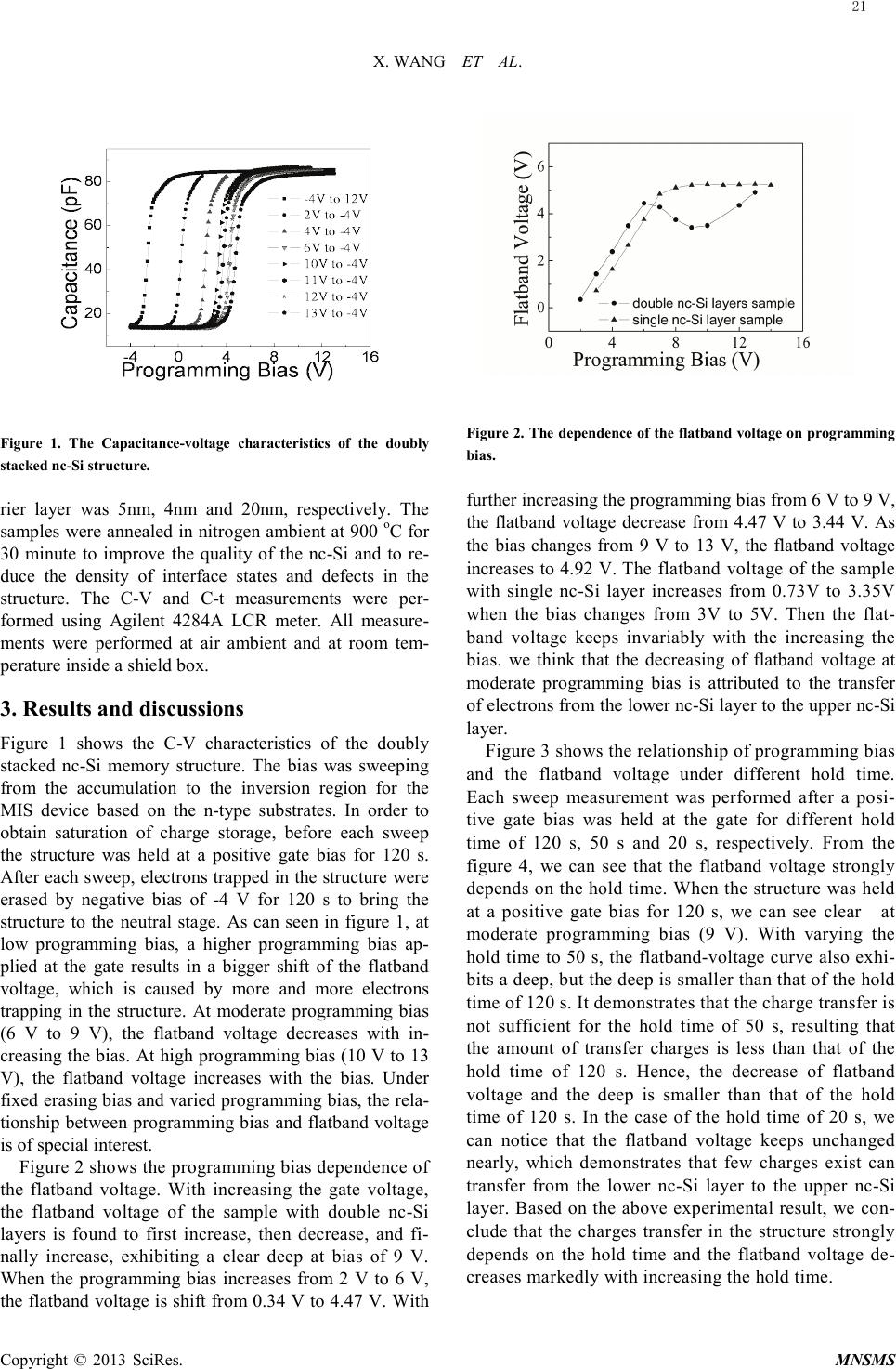 X. WANG ET AL. Copyright © 2013 SciRes. MNSMS Figure 1. The Capacitance-voltage characteristics of the doubly stacked nc-Si structure. rier layer was 5nm, 4nm and 20nm, respectively. The samples were annealed in nitrogen ambient at 900 oC for 30 minute to improve the quality of the nc-Si and to re- duce the density of interface states and defects in the structure. The C-V and C-t measurements were per- formed using Agilent 4284A LCR meter. All measure- ments were performed at air ambient and at room tem- perature inside a shield box. 3. Results and discussions Figure 1 shows the C-V characteristics of the doubly stacked nc-Si memory structure. The bias was sweeping from the accumulation to the inversion region for the MIS device based on the n-type substrates. In order to obtain saturation of charge storage, before each sweep the structure was held at a positive gate bias for 120 s. After each sweep, electrons trapped in the structure were erased by negative bias of -4 V for 120 s to bring the structure to the neutral stage. As can seen in figure 1, at low programming bias, a higher programming bias ap- plied at the gate results in a bigger shift of the flatband voltage, which is caused by more and more electrons trapping in the structure. At moderate programming bias (6 V to 9 V), the flatband voltage decreases with in- creasing the bias. At high programming bias (10 V to 13 V), the flatband voltage increases with the bias. Under fixed erasing bias and varied programming bias, the rela- tionship between programming bias and flatband voltage is of special interest. Figure 2 shows the programming bias dependence of the flatband voltage. With increasing the gate voltage, the flatband voltage of the sample with double nc-Si layers is found to first increase, then decrease, and fi- nally increase, exhibiting a clear deep at bias of 9 V. When the programming bias increases from 2 V to 6 V, the flatband voltage is shift from 0.34 V to 4.47 V. With Figure 2. The dependence of the flatband voltage on programming bias. further increasing the programming bias from 6 V to 9 V, the flatband voltage decrease from 4.47 V to 3.44 V. As the bias changes from 9 V to 13 V, the flatband voltage increases to 4.92 V. The flatband voltage of the sample with single nc-Si layer increases from 0.73V to 3.35V when the bias changes from 3V to 5V. Then the flat- band voltage keeps invariably with the increasing the bias. we thi nk that the decreasing of flatband voltage at moderate programming bias is attributed to the transfer of electrons from the lower nc-Si layer to the upper nc-Si layer . Figure 3 shows the relationship of programming bias and the flatband voltage under different hold time. Each sweep measurement was performed after a posi- tive gate bias was held at the gate for different hold time of 120 s, 50 s and 20 s, respectively. From the figure 4, we can see that the flatband voltage strongly depends on the hold time. When the structure was held at a positive gate bias for 120 s, we can see clear at moderate programming bias (9 V). With varying the hold time to 50 s, the flatband-voltage curve also exhi- bits a deep, but the deep is smaller than that of the hold time of 120 s. It demonstrates that the charge transfer is not sufficient for the hold time of 50 s, resulting that the amount of transfer charges is less than that of the hold time of 120 s. Hence, the decrease of flatband voltage and the deep is smaller than that of the hold time of 120 s. In the case of the hold time of 20 s, we can notice that the flatband voltage keeps unchanged nearly, which demonstrates that few charges exist can transfer from the lower nc-Si layer to the upper nc-Si layer. Based on the above experimental result, we con- clude that the charges transfer in the structure strongly depends on the hold time and the flatband voltage de- creases markedly with increasing the hold time. 21 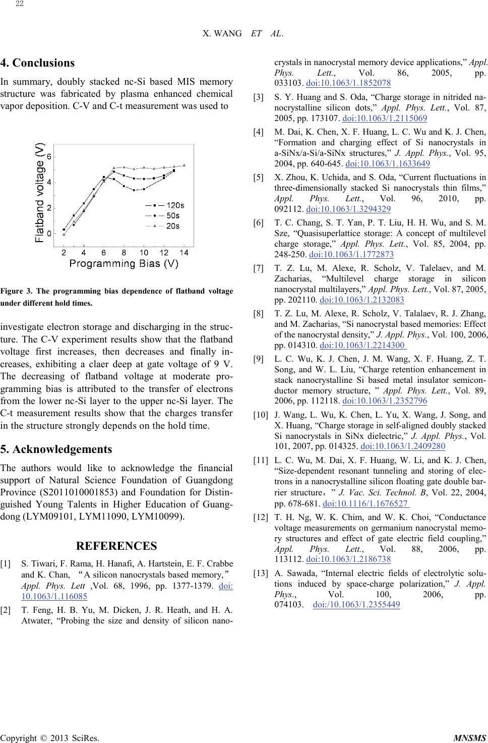 X. WANG ET AL. Copyright © 2013 SciRes. MNSMS 4. Conclusions In summary, doubly stacked nc-Si based MIS memory structure was fabricated by plasma enhanced chemical vapor deposition. C-V and C-t measurement was used to Figure 3. The programming bias dependence of flatband voltage under different hold times. investigate electron storage and discharging in the struc- ture. The C-V experiment results show that the flatband voltage first increases, then decreases and finally in- creases, exhibiting a claer deep at gate voltage of 9 V. The decreasing of flatband voltage at moderate pro- gramming bias is attributed to the transfer of electrons from the lower nc-Si layer to the upper nc-Si layer. The C-t measurement results show that the charges transfer in the structure strongly depends on the hold time. 5. Acknowledgemen t s The authors would like to acknowledge the financial support of Natural Science Foundation of Guangdong Province (S2011010001853) and Foundation for Distin- guished Young Talents in Higher Education of Guang- dong (LYM09101, LYM11090, LYM10099). REFERENCES [1] S. Tiwari, F. Rama, H. Hanafi, A. Hartstein, E. F. Crabbe and K. Chan, “A silicon nanocrystals based memory,” Appl. Phys. Lett ,Vol. 68, 1996, pp. 1377-1379. doi: 10.1063/1.116085 [2] T. Feng, H. B. Yu, M. Dicken, J. R. Heath, and H. A. At water , “Probing the size and density of silicon nano- crystals in nanocrystal memory device applications,” Appl. Phys. Lett., Vol. 86, 2005, pp. 033103. doi:10.1063/1.1852078 [3] S. Y. Huang and S. Oda, “Charge storage in nitrided na- nocrystalline silicon dots,” Appl. Phys. Lett., Vol. 87, 2005, pp. 173107. doi:10.1063/1.2115069 [4] M. Dai, K. Chen, X. F. Huang, L. C. Wu and K. J. Chen, “Formation and charging effect of Si nanocrystals in a-SiNx/a-Si/a-SiNx stru ctures,” J. Appl. Phys., Vol. 95, 2004, pp. 640-645. doi:10.1063/1.1633649 [5] X. Zhou, K. Uchida, and S. Oda, “Current fluctuations in three-dimensionally stacked Si nanocrystals thin films,” Appl. Phys. Lett., Vol. 96, 2010, pp. 092112. doi:10.1063/1.3294329 [6] T. C. Chang, S. T. Yan, P. T. Liu, H. H. Wu, and S. M. Sze, “Quasisuperlattice storage: A concept of multilevel charge storage,” Appl. Phys. Lett., Vol. 85, 2004, pp. 248-250. doi:10.1063/1.1772873 [7] T. Z. Lu, M. Alexe, R. Scholz, V. Talelaev, and M. Zacharias , “Multilevel charge storage in silicon nanocrystal multilayers,” Appl. Phys. Lett., Vol. 87, 2005, pp. 202110. doi:10.1063/1.2132083 [8] T. Z. Lu, M. Alexe, R. Scholz, V. Talalaev, R. J. Zhang, and M. Zacharias, “Si nanocrystal based memories: Effect of the nanocrystal density,” J. Appl. Phys., Vol. 100, 2006, pp. 014310. doi:10.1063/1.2214300 [9] L. C. Wu, K. J. Chen, J. M. Wang, X. F. Huang, Z. T. Song, and W. L. Liu, “Charge retention enhancement in stack nanocrystalline Si based metal insulator semicon- ductor memory structure, ” Appl. Phys. Lett., Vol. 89, 2006, pp. 112118. doi:10.1063/1.2352796 [10] J. Wang, L. Wu, K. Chen, L. Yu, X. Wang, J. Song, and X. Huang, “Charge storage in self-aligned doubly stacked Si nanocrystals in SiNx dielectric,” J. Appl. Phys., Vol. 101, 2007, pp. 014325. doi:10.1063/1.2409280 [11] L. C. Wu, M. Dai, X. F. Huang, W. Li, and K. J. Chen, “Size-dependent resonant tunneling and storing of elec- trons in a nanocrystalline silicon floating gate double bar- rier structure,” J. Vac. Sci. Technol. B, Vol. 22, 2004, pp. 678-681. doi:10.1116/1.1676527 [12] T. H. Ng, W. K. Chim, and W. K. Choi, “Conductance voltage measurements on germanium nanocrystal memo- ry structures and effect of gate electric field coupling,” Appl. Phys. Lett., Vol. 88, 2006, pp. 113112. doi:10.1063/1.2186738 [13] A. Sawada, “Internal electric fields of electrolytic solu- tions induced by space-charge polarization,” J. Appl. Phys., Vol. 100, 2006, pp. 074103. doi:/10.1063/1.2355449 22 |